7. Electronics design
This week I worked on learing more on electronics followed by creating our own circut board.
Group Work
Process
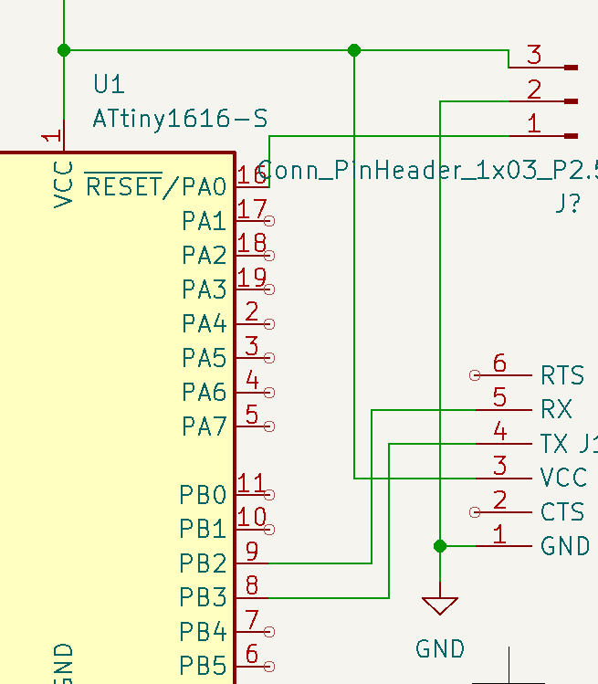
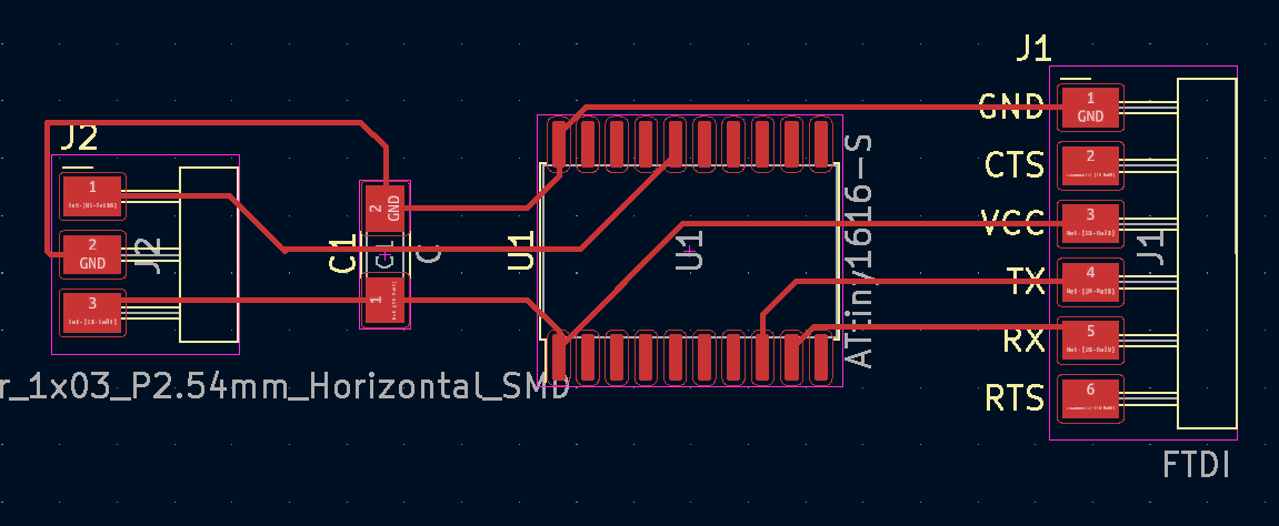
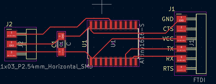
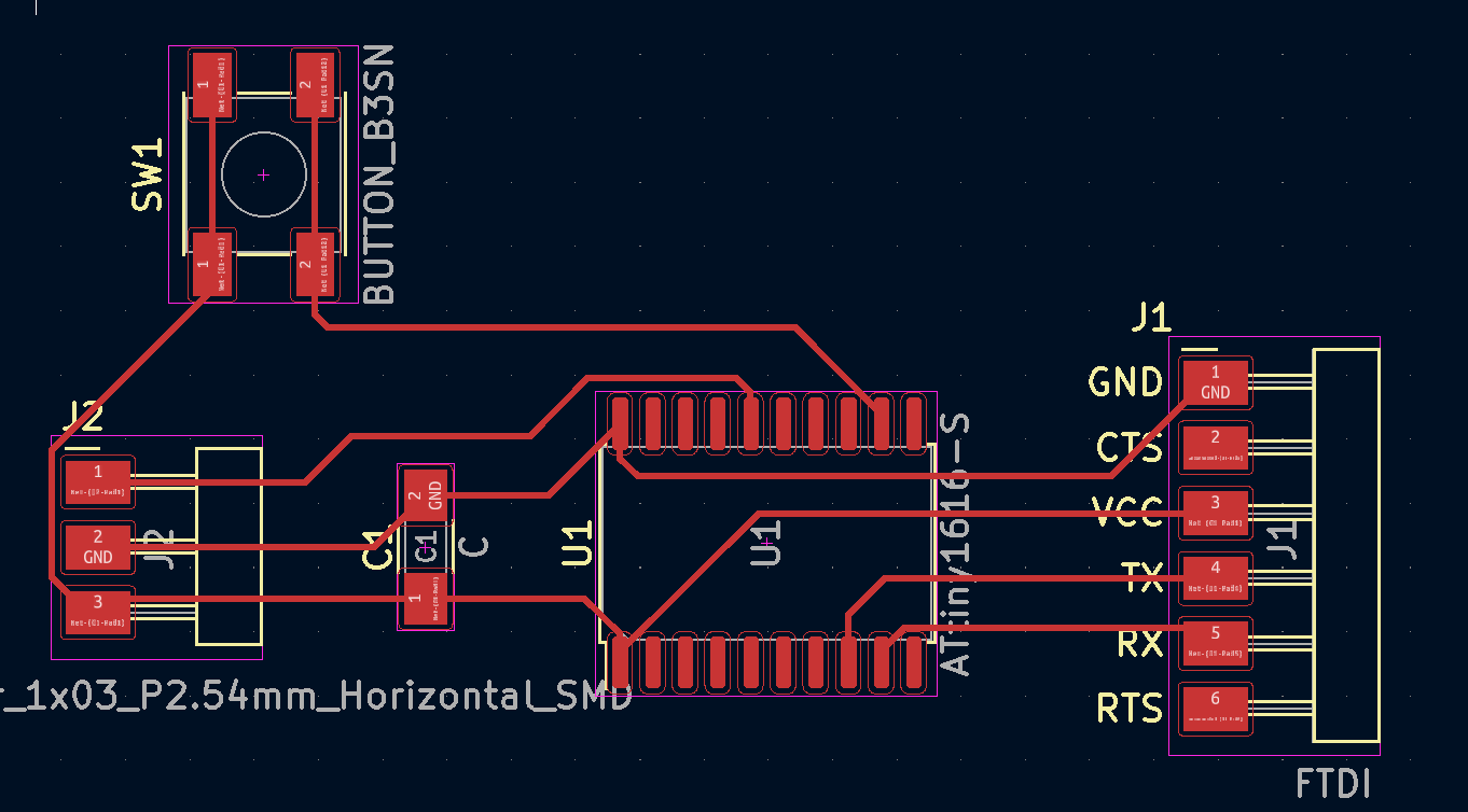
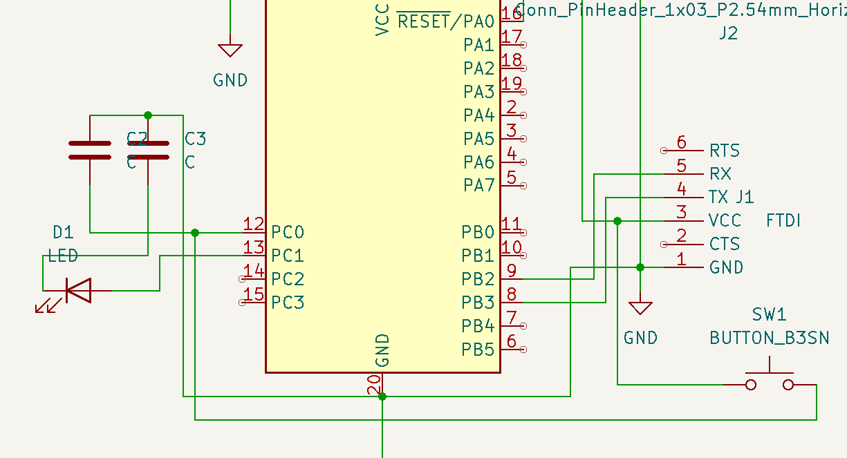
The Kicad process started by creating a new file which in turn creates the two interfaces I will be working on first is the schematic where I find each part I want and connect them together. Second is the PCB editor where I design the set up of the board.
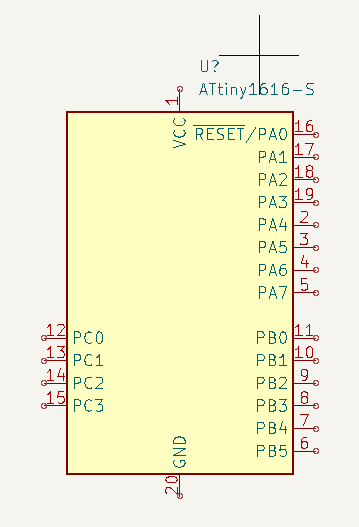
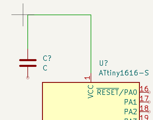
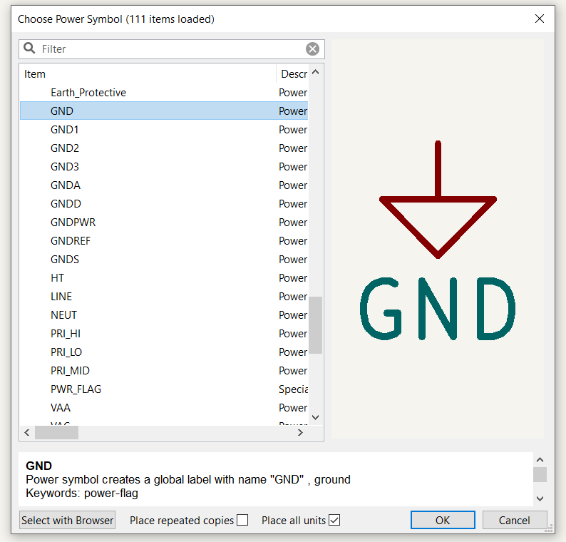
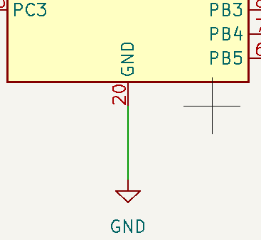
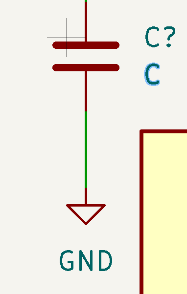
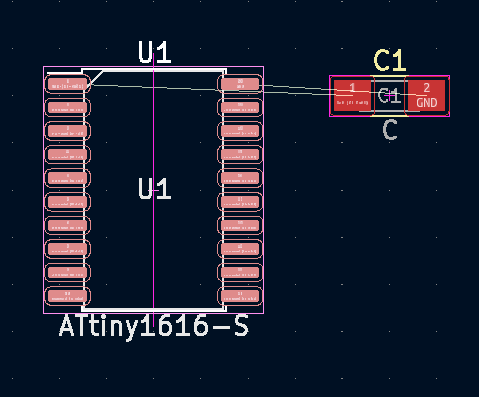
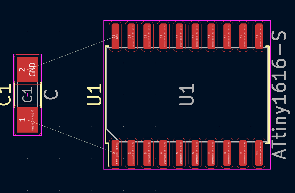
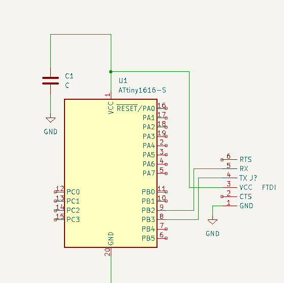
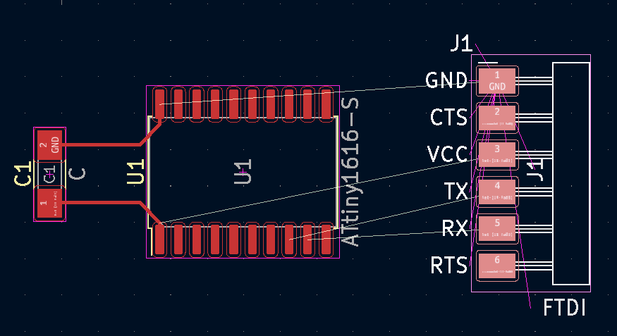
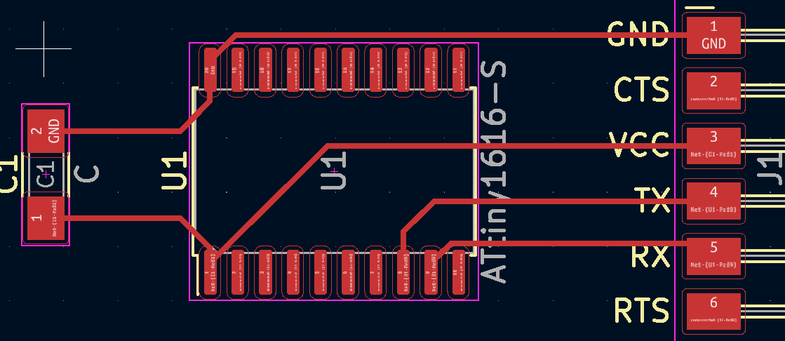
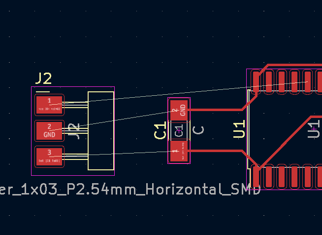
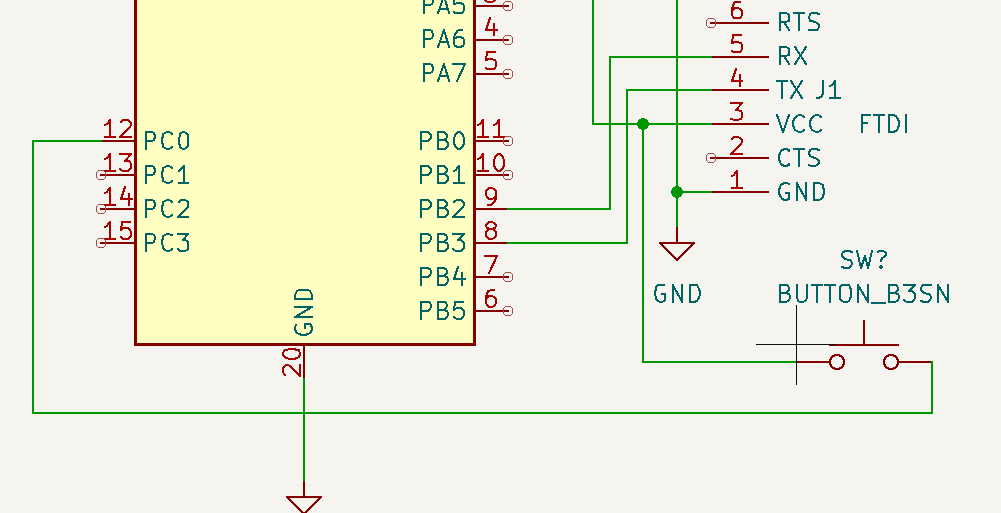
 The first three things I had to do was set up the board I would using in this case it is an Attiny 1616. I would then rig a capacator to my VCC on pin 1 and then set up my ground on pin 20 and connect my capacator to ground. In order to get my ground much like all my other parts I went to the libarary and selected it.
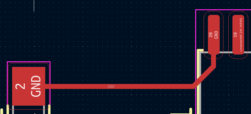
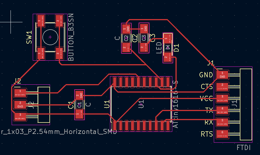
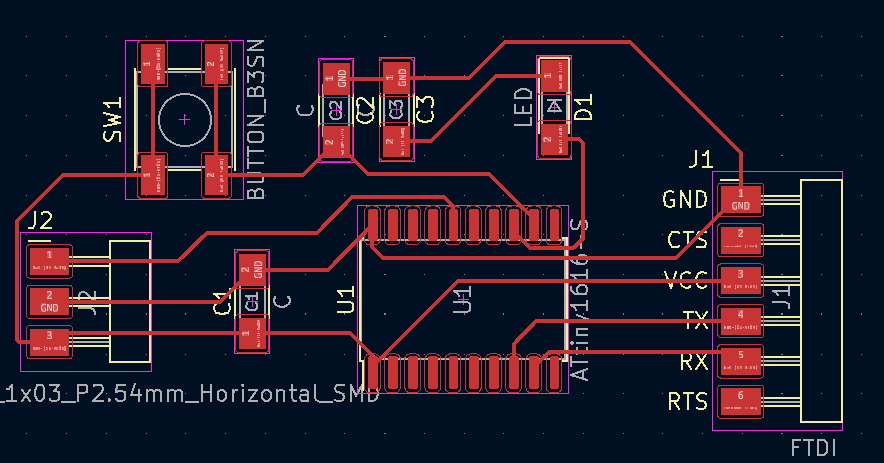
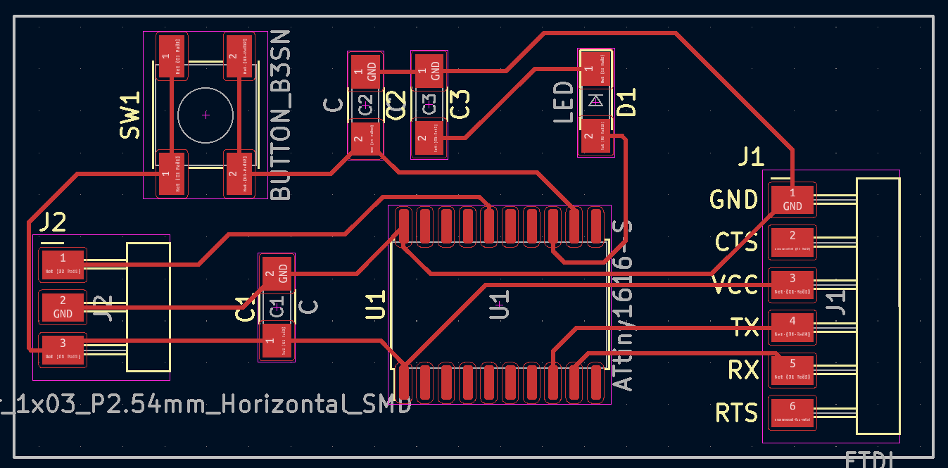
 The next thing I would do is go to my PCB editor to connect my routes and change the placement of my parts. It needs to be noted that while making routes it can at times be like a puzzle because you don’t want paths to cross and sometimes you need to be really creative with your set up. Luckily the PCB editor has helpful lines showing you what needs to be connected.

After completing my board design I moved onto milling out my board. The milling process had numerous issues with ripping up my board which was due to human error I initially hadn’t used a ball nosed bit. I would get a successful board created and then saudered but unfortunatley there were issues with this as well.
No matter what I did the board would not program