4. Electronics production
Goal of the week:
Individual Assignment:
- Make an in-circuit programmer by milling and stuffing the PCB
Group assignments:
- Characterize the design rules for your PCB production process: document feeds, speeds, plunge rate, depth of cut (traces and outline) and tooling.
- Document your work (in a group or individually).
You can find the documentation about week 4 group assignment here.
Individual Assignment:
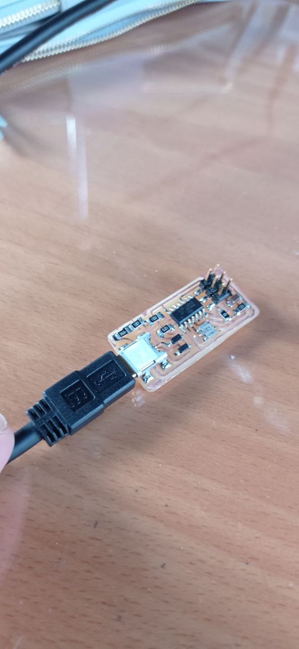
Basically, what we had to do this week was to create an ISP (in-system programming) to be used to program all the boards we will develop in the future. We could choose among several already-made examples. We had to replicate one of them by milling, after that we had to stuff the different components, then you had to check if everything worked well and finally program it.
I decided to work on the Ali’s FabISP. I went on his page and downloaded the png files traces and outline. I had to use the second version, the one with two different resistors (1K Ohm plus 0.5 K Ohm because in the lab we don’t have a resistor of 1,5 K ohm)
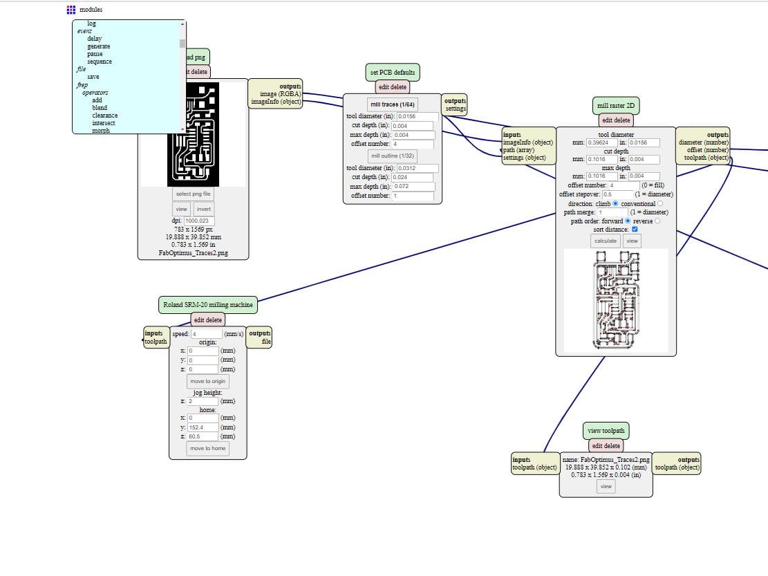
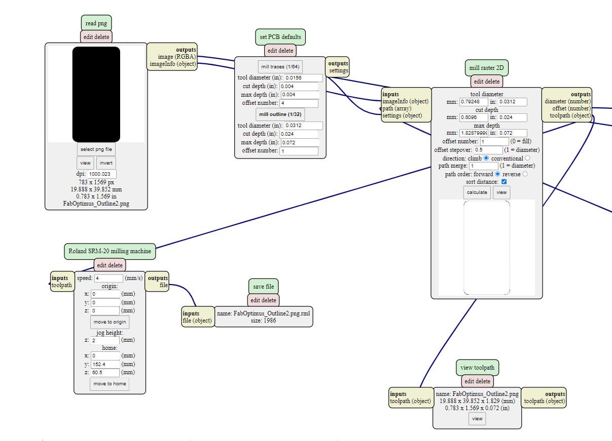
I used the Fab modules to generate the cutting files and download the .rml files.
The command I gave at the beginning to the mods was Program –> Open server program –> Machines –> Roland –> mill –> SRM-20 –> PCB png A screen appeared with several blocks of settings to program.
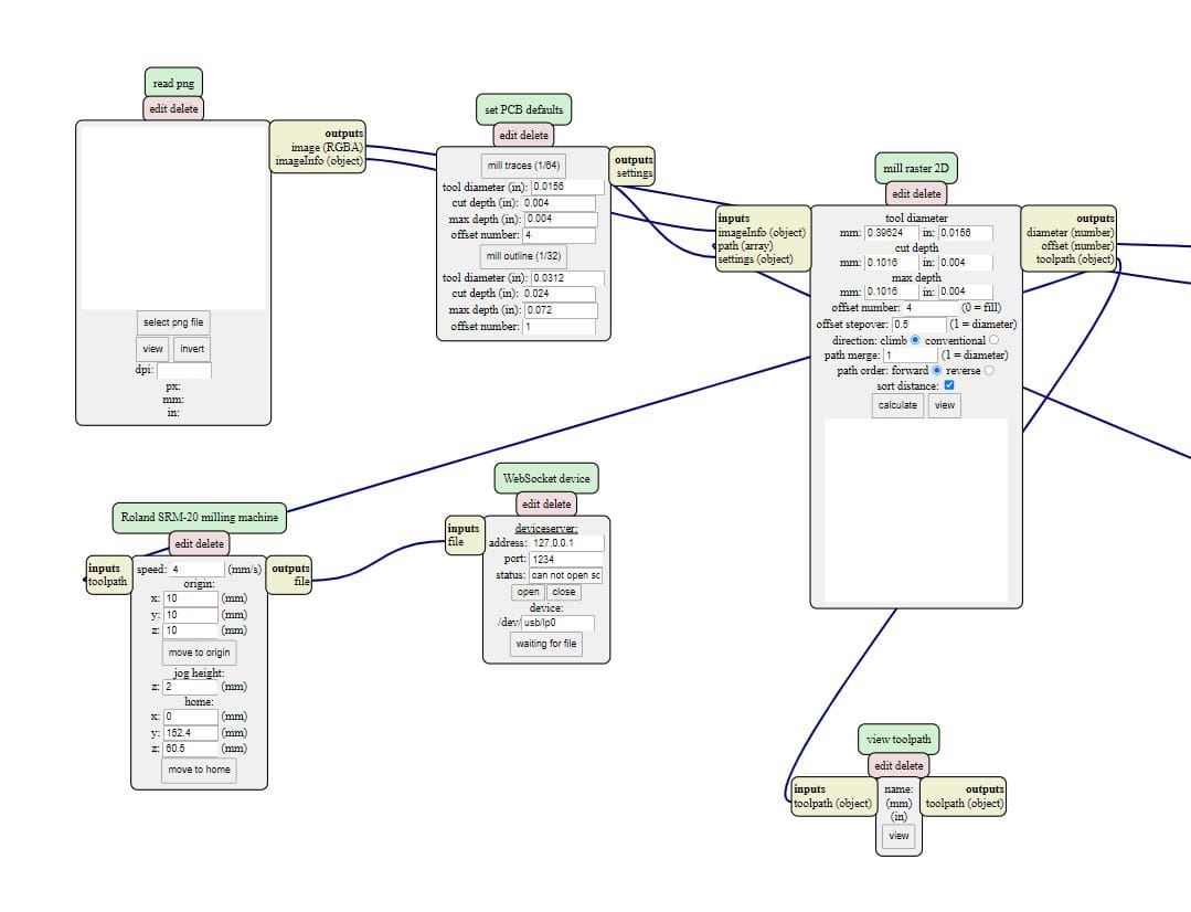
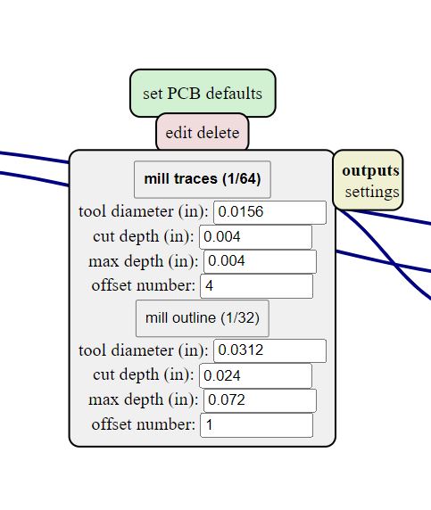
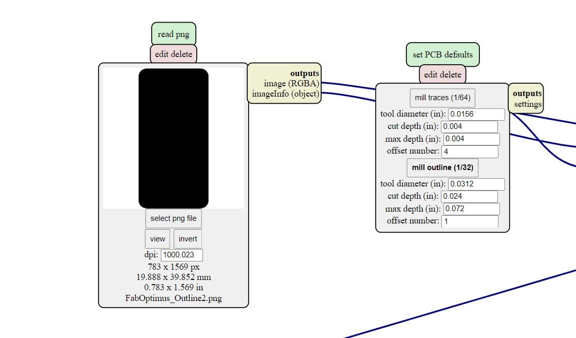
Then I loaded the traces.png. I choose mill traces (1/64) in set PCB defaults panel and I left all the settings as default.
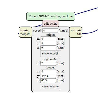
The only value that I changed was the origin X, Y, Z voice inside Roland SRM-20 milling machine panel. I replaced 10 with 0, defining a new starting point for the machine.
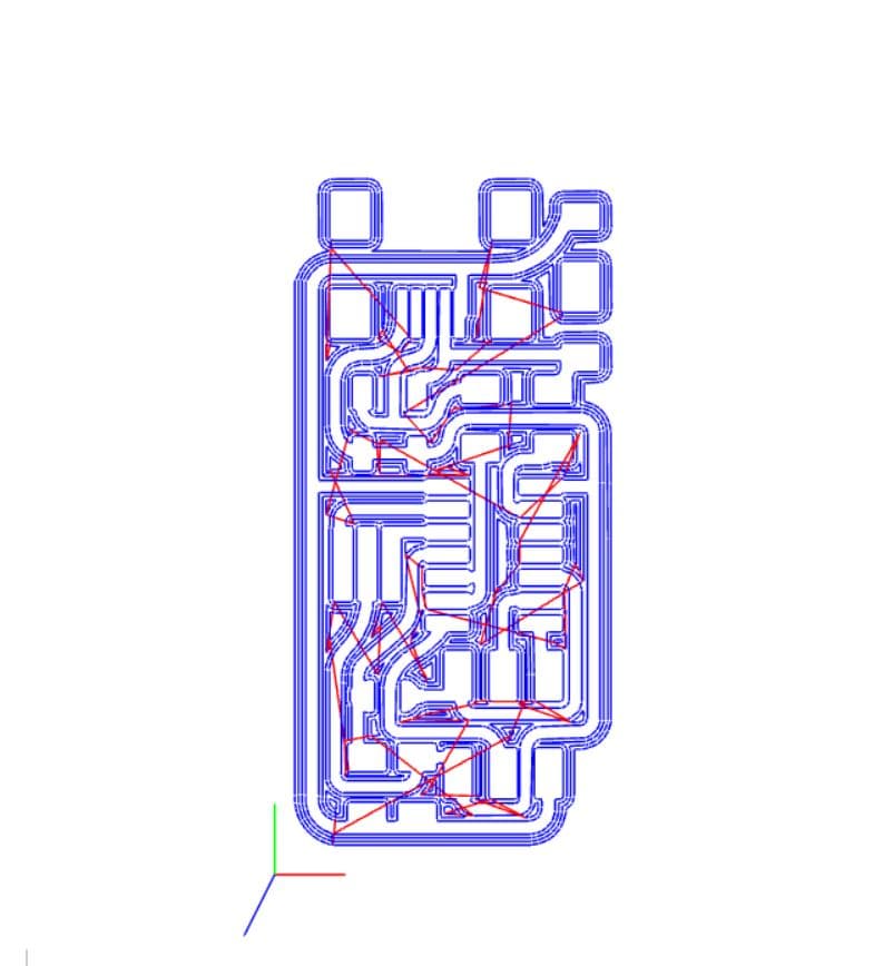
Then, in the mill raster 2D panel I clicked on calculate and I was able to see the cutting file of the traces.
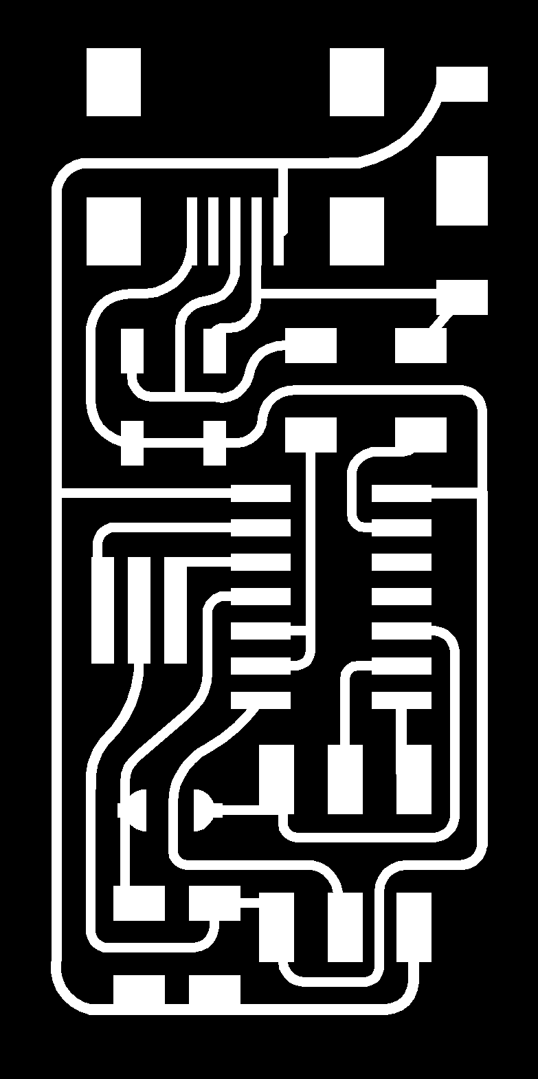
To check if everthing worked I clicked on the view voice and an image like the one below appeared.
The last thing to do was to delete the WebSocketDevice panel and replace it with another block to save the file in .rml format. I went on Module–>Add server module–>file->save and linked it in the right position. After clicking again on “calculate” the program automatically downloaded the traces file.
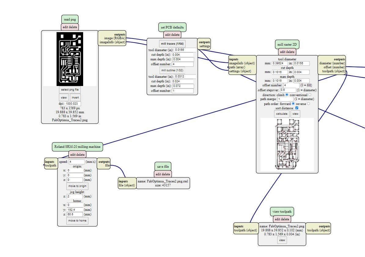
After that, I did the same process with the outline file, except for set PCB defaults values: in fact I choose 1/32 of inch tip.
MILLING
After this first (and quite easy) step, we started to have the first problems.
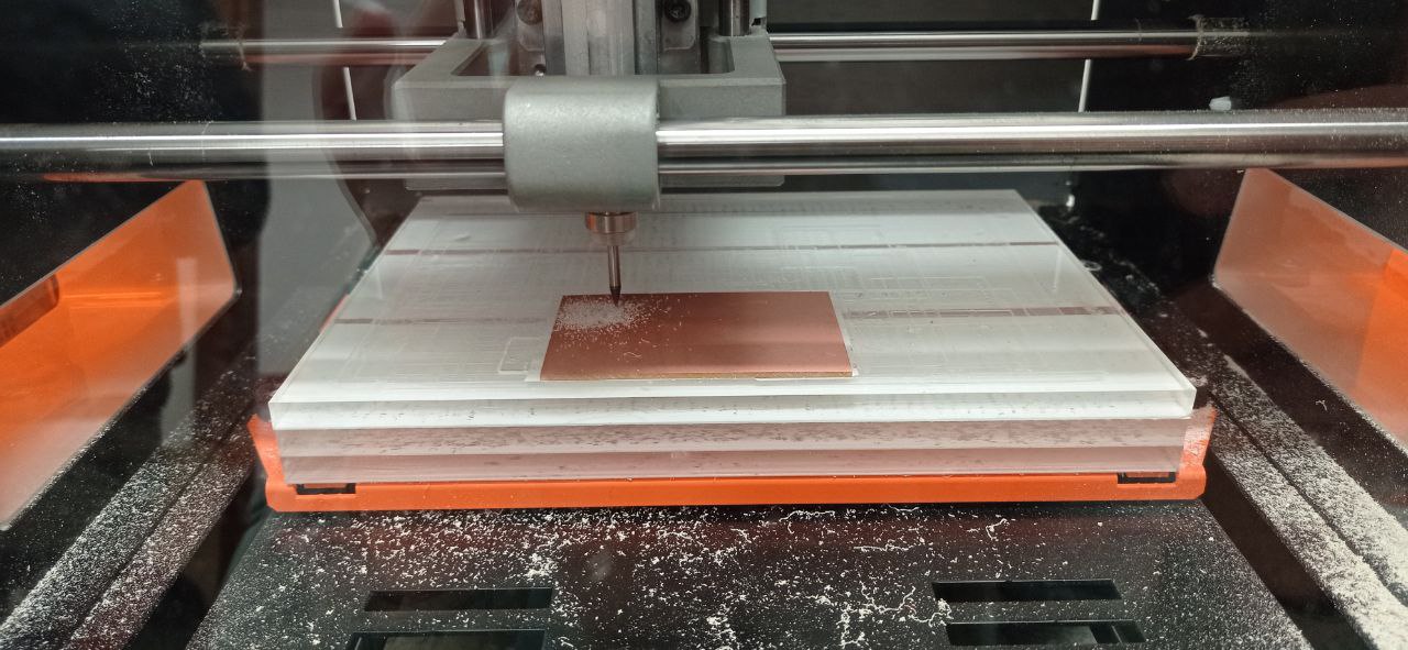
The first of us that tried to milling made a fatal error with the tip. In this work it’s important to be really careful with the tip header, especially with the smaller one (1/64). During the milling you have change the bit with a specific key and screw clockwise to block it.
Well…the problem was perhaps too much caution and fear of breaking the tip. The result was that not too much force was applied to block the bit and therefore halfway through the first milling, it collapsed on the board, blocking everything and slightly damaging the machine.
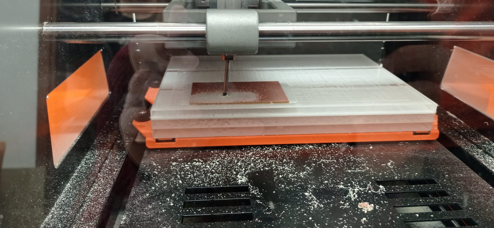
So at this point, for all subsequent work, we used an old bit… It wasn’t perfect but it still did its job!
Anyway, the tips to do a well done job are:
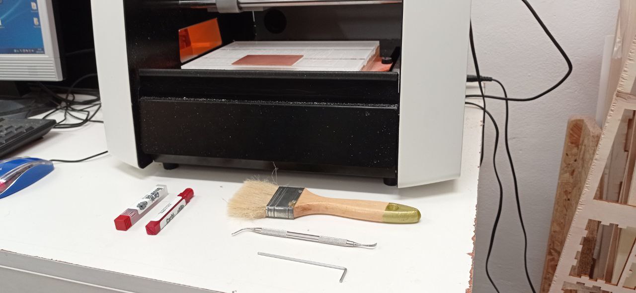
- Clean the sacrificial layer from all the dust of the previous works
- Use double-sided tape on the Plexiglas sacrificial layer and stick the board firmly.
- Set 1/64 tip first (with caution but not too much!) and after milling the traces change it with the 1/32 tip for the outline.
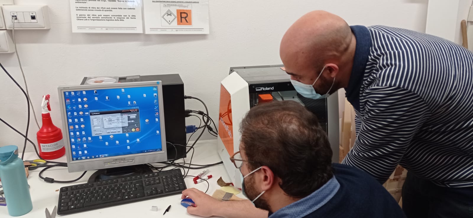
To send command to the machine we used VPanel for SRM-20.
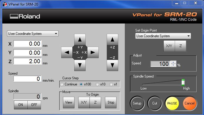
First step was to set the origin: its position should be in the bottom left of your workspace. Once you positioned physically X,Y and Z as you want, tell the machine that point is the origin. Then click on Cut button and add the .rml files…and cross your finger!
My work was quite complicated and I had to repeat it three times.
On the first attempt, the board moved, changing the direction of some of the tracks. On the second attempt, the tip was probably inserted the wrong way and therefore not touching the board properly, not being able to engrave the traces correctly. I stopped the machine and proceeded with a third attempt.
Everything seemed to go correctly when, as the machine began to engrave the outline, after the first round the board detached from the sacrificial plate and began to move. I immediately stopped the machine and continued the engraving operation with a cutter. It was a hard work but in the end I managed to get my board.
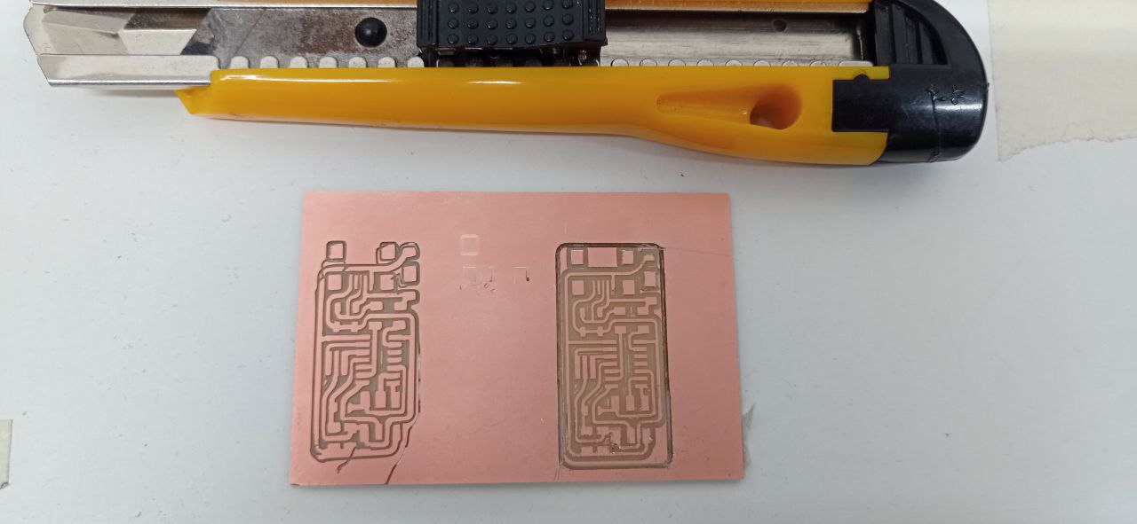
Probably the mistake was because the sacrificial plate was very worn and uneven so in the lower part the machine could not engrave properly. The solution I should have adopted would have been to put more tape, chose a better position and clean the layer more thoroughly.
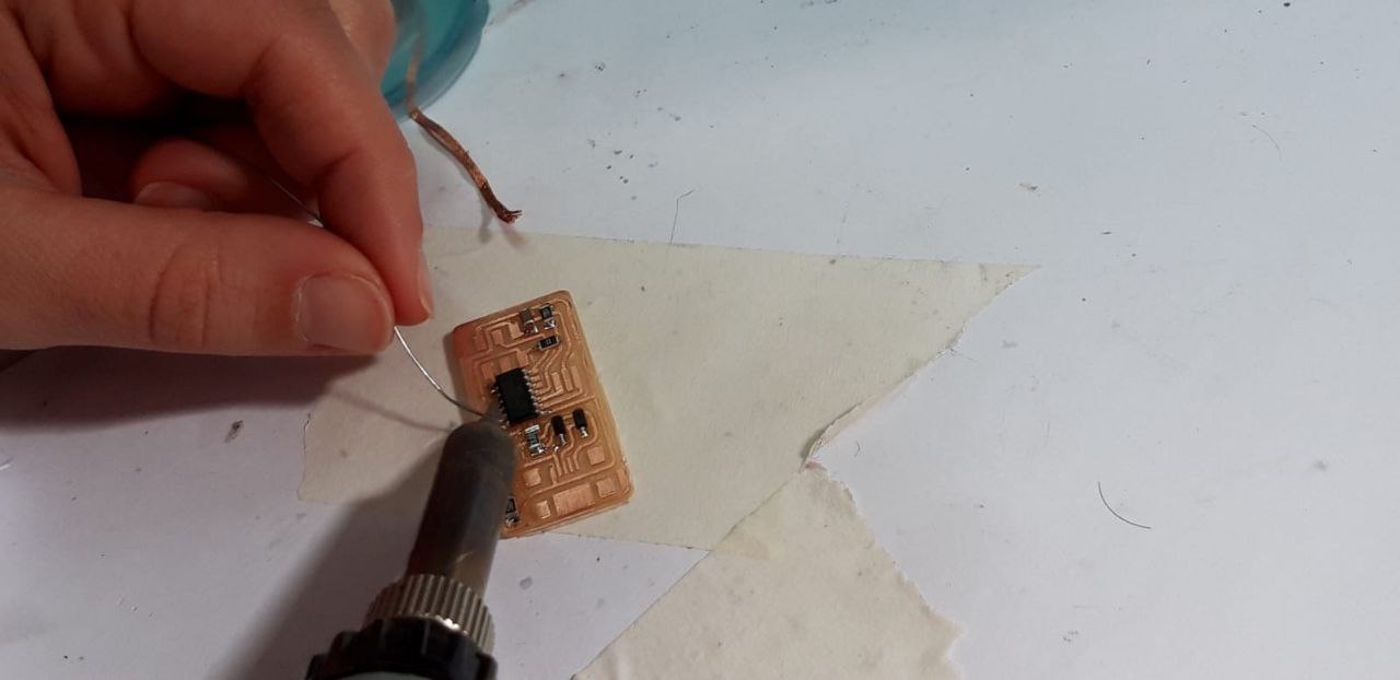
After cleaning it with sandpaper, washing it with soap and checking that all the tracks were present and well connected, I started the soldering.
SOLDERING
I thought soldering would be the hardest part, but at the end it was also quite fun and challenging.
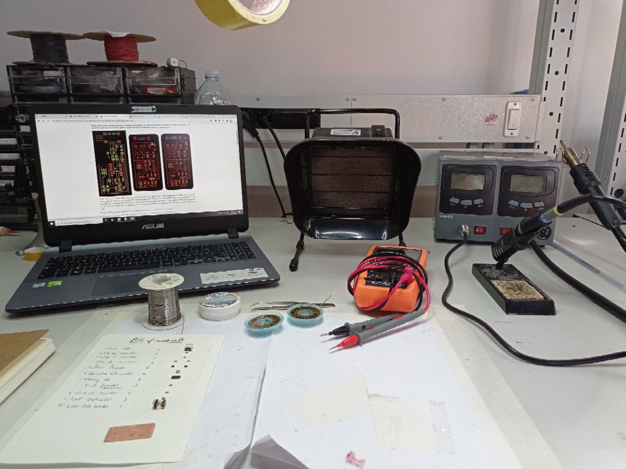
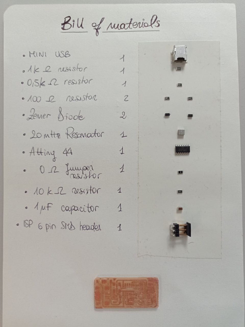
Despite the trembling of my hands and my poor eyesight, with the help of a magnifying glass and a lot of patience I gathered all the components I needed and put them in the bill of materials.
I then started soldering from the smallest components in the central part and moving gradually to the larger components.
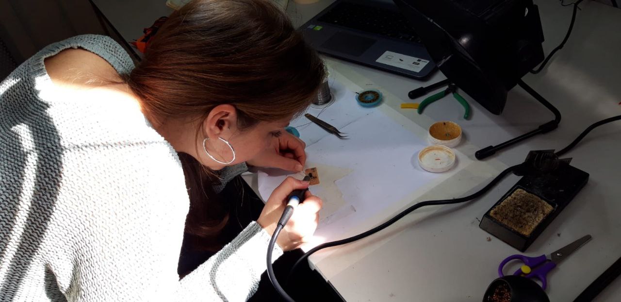
After a long hour of concentration and deep breaths, I managed to solder the entire board.
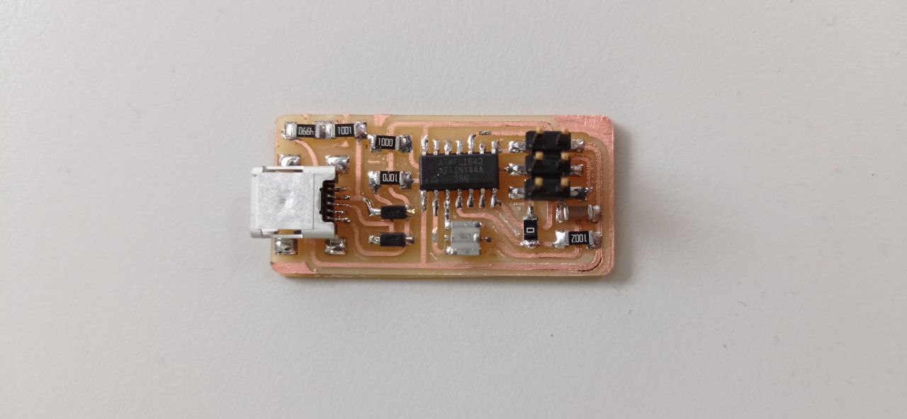
I then used a multimeter to check that the traces and components continued to conduct energy after soldering. Then, following the advice of my instructor, we did the smoking test, connecting the board with a cable to the power supply. If the soldering was not successful there would be a short circuit and therefore smoke.
Breath of relief
PROGRAMMING
As the last part of the assignment, it was necessary to program the PCB and transform it in a programmer. To do so, I followed the steps that FabAcademy tutorial suggest me. Basically:
- Install the toolchain and download the firmware.
- Edit the Makefile
- Program the board
- Verify if everything works well
- Open up the jumpers (desolder the 0 ohm resistor) to make it a programmer.
AVR TOOLCHAIN
The steps to download the toolchain are:
-
Download the AVR toolchain (for Windows 10 in my case). This is a COMPILER, that turn your source code in a machine one. To download it you have to log in Microchip site and download the version that you need. You’ll get a .zip file.
-
Download GNU make. A makefile is used to automate all the repetitive, intermediate bits of the process.
-
Download AVRdude, a software uploader that send the machine code in your PCD, storing all the information in its nonvolatile flash memory. I download it from this tutorial
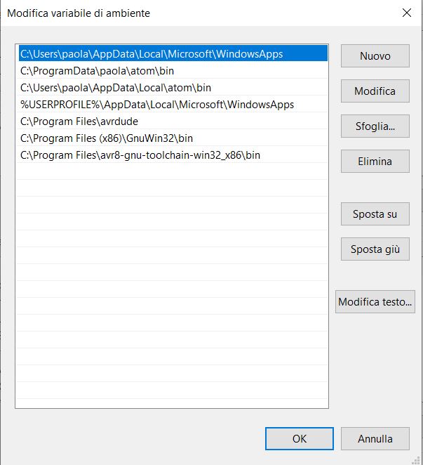
Be careful where you put your unzip files! At this point we need to tell Windows where to locate all of the tools you’ve just installed when you type their names on the command line. The commands to do that are: Start menu –> Control Panel –> System –> Advanced System Settings. Click the “Environment Variables” button. Under User variables, select _Path –> New__ and you can enter a new Path. Click Ok in all the windows we opened.
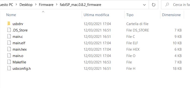
After that, I downloaded the firmware, in other world I downloaded the software that will program my PCB. I unzip the file and put it in a fold on my desktop. Then, I clicked on the folder, then on fabISP_mac.0.8.2_firmware –> Makefile
I opened the Makefile on my editor and (as the tutorial suggested) I changed some lines. In particular, I changed the comment(#) from the upper line, down to the following line. This because my PCB was an “attiny”, ad not an “avrisp2”. Then I inverted the “#” and saved the file.

In GIT BASH I inserted the command make -v, avrdude -v to stamp the content of the software. The terminal did not issue any errors
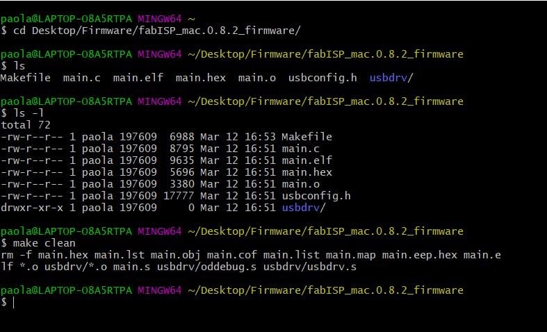
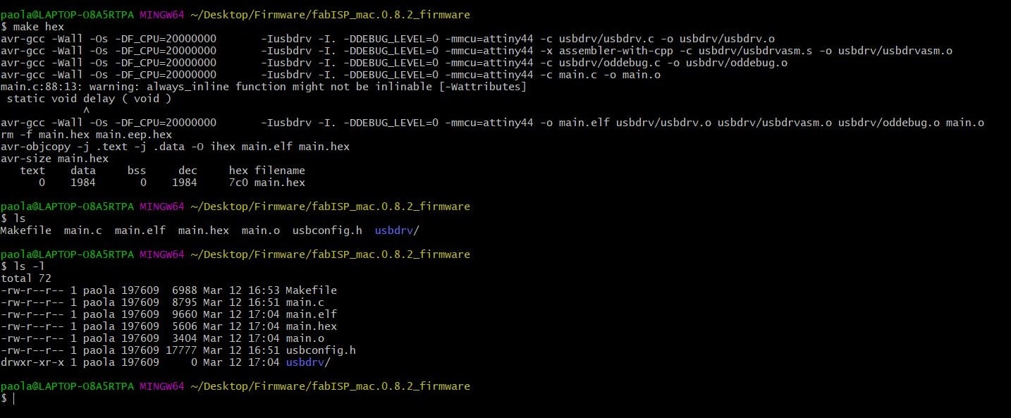
Next step was to compile the firmware, transforming it into a machine-understandable language. I connected my PCB to a commercial programmer and then I connect the programmer to my computer. With the commands Control panel -> system -> device manager I checked if my computer could recognize the programmer. Then I went on GIT BASH inside the makefile folder. I used the command make clean to clean up my PCB:
Then make hex to transform the .c file in a .hex readable for the machine:
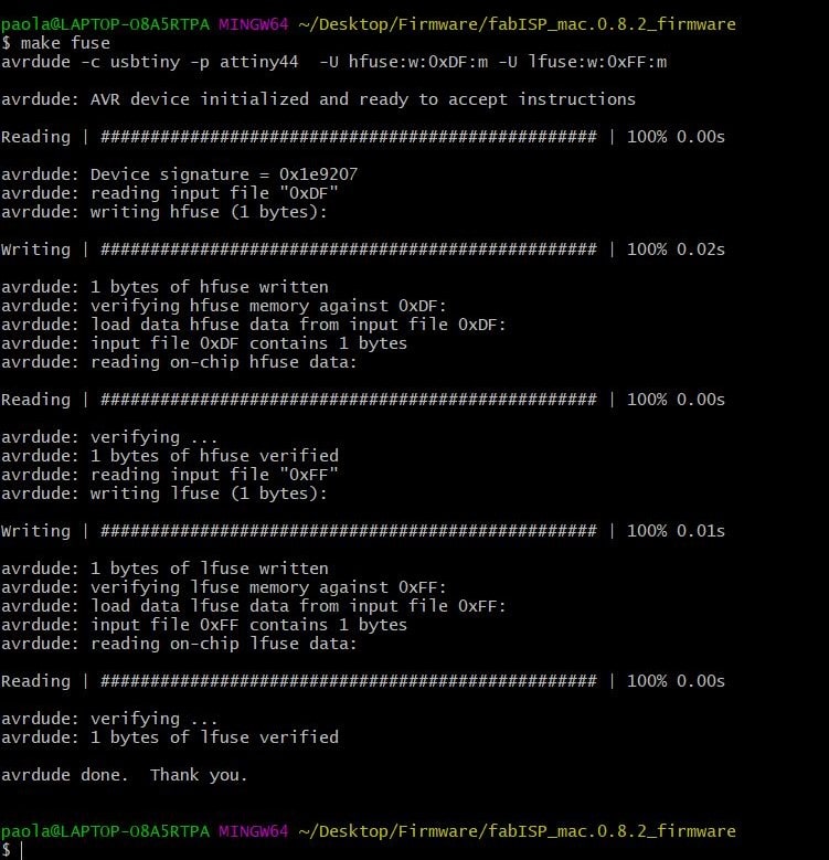
Next, with the command make fuse I set the fuses so your board will use the external clock (crystal)
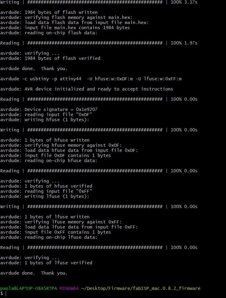
And at the end I programmed my board typing make program
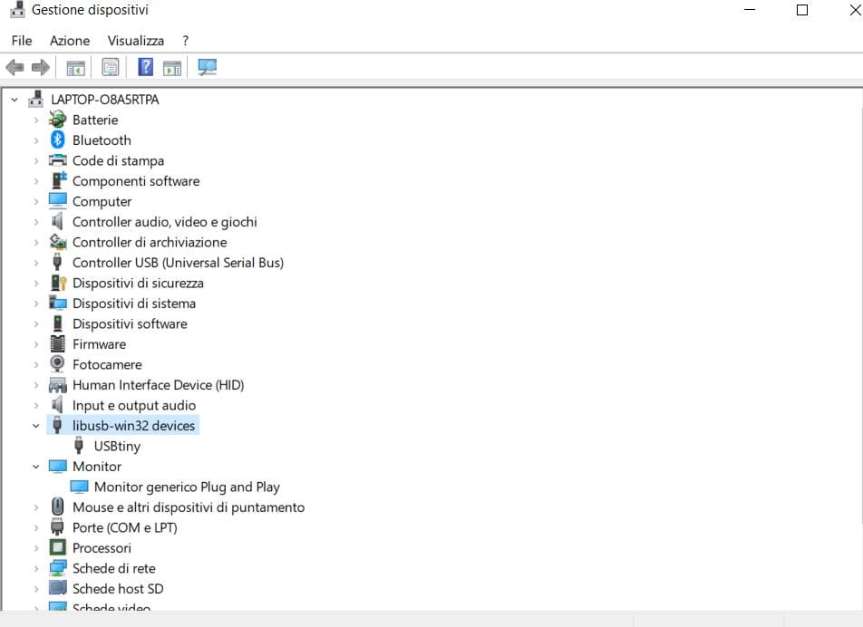
To verify if everything worked well and my ISP is working correctly I went on control panel –> system –> device management
Last step: remove the solder bridge (the 0 ohm resistor) to use the programmer to program other boards.