Electronics Production
Week 05
The fifth week was about PCB production process. In the group assignment, we had to characterize the design rules for our PCB production process. After that our individual assignment was about to make an in-circuit programmer by milling the PCB.
What is a PCB?
A PCB, acronym for Printed Circuit Board, is nothing else than a carrier for electronic components. The PCB is used as a mechanical mounting and enables electrical connections to be established through structuring.
The final goal is to produce conductive traces on the printed circuit board through structuring, which are built on an electrically insulating material. As a material one often uses FR1 to FR4, of course, there are countless other materials. There are different ways to produce these PCBs. One is etching, here however in the prototype area one uses the production utilizing a CNC milling machine for small structured work. Producing different variations of the printed circuit board is possible. For me, the one-sided and two-sided printed circuit boards will come into question for my final project. It makes sense to use this here because the electrical transmission and reliability are much higher compared to a breadboard. The additional effort is low - it is much fun. Within the Fab Academy, the boards should also not be equipped with boring parts: SMDs are unwired components and are soldered directly onto them. They are surface mounted and therefore have their name: Surface Mounted Devices, SMD for short. Of course, they contribute to the fact that all devices in the world are getting smaller and smaller. It’s unbelievable hard to even grab the small 0402-SMD-part (0,5mm width) and if you lose one on the ground - you don’t need to search for them, it’s nearly impossible to find, especially on a carpet. In the following weeks I preferred to use the 1206-SMD-parts with a width of 1,2mm. At the end, it makes a lot of fun to solder the SMD-parts on a PCB.
In order to build a PCB prototype with up to two layers, it is a very good solution to make the board in-house yourself. This is also described in the following documentation. Another option, which is commonly used, is to order it from an external service provider. A well-known possibility is for example JLCPCB.
Software-choice: EAGLE or KiCAD?
The actual process of creating a prototype is to use a breadboard and connect everything. This way all components are provisionally connected. Nevertheless, if you want to finalize the project, it makes sense to create a PCB and design it by using a PCB-software.
The first question is of course: Which software should I use?
There are several software solutions. I want to go into two of them in more detail. The first is a software called EAGLE by Autodesk, which has been on the market for more than 25 years (EAGLE stands for Easily Applicable Graphical Layout Editor). Formerly still by Cadsoft, but then bought by Autodesk a few years ago and still available for hobby use as free software with limitations. You can find many libraries and files online, especially from the open-source field. If you open the program for the first time you are overwhelmed by the usability. So much user-centered design can only rarely be found (joke). The software is a powerful and an excellent solution. The connection with other Autodesk software is given. This makes it possible, for example, to export the model to Fusion 360, so that you could directly draw a housing for your PCB.
The second software I considered was KiCAD. KiCAD is entirely open-source and also an extensive tool. There are excellent training videos, more and more open-source projects, as well as the Arduino boards reference designs, switch to KiCAD.
However, for me the decision was straightforward: Everyone from my environment is using EAGLE. So if I need help, which I will definitely need, I should use EAGLE. But as a todo for the end of the year, KiCAD will still be on the learning list.
EAGLE - schematic
To create a PCB design, you have to do two things. First, you have to create a schematic design and then transfer it to a reasonable board layout. It’s something exciting, that the board design and the schematic design work hand in hand.
For this, I use EAGLE and get the following overview as it is shown in the picture. First of all the user interface and the control elements are difficult to understand. But if you take your time and get used to EAGLE, you will notice that it is easier than you thought at the beginning. For that I watched some tutorials, which you can find good videos on the youtube channel from Autodesk EAGLE. More good links you can find in the documentation of week 07 - electronic design.
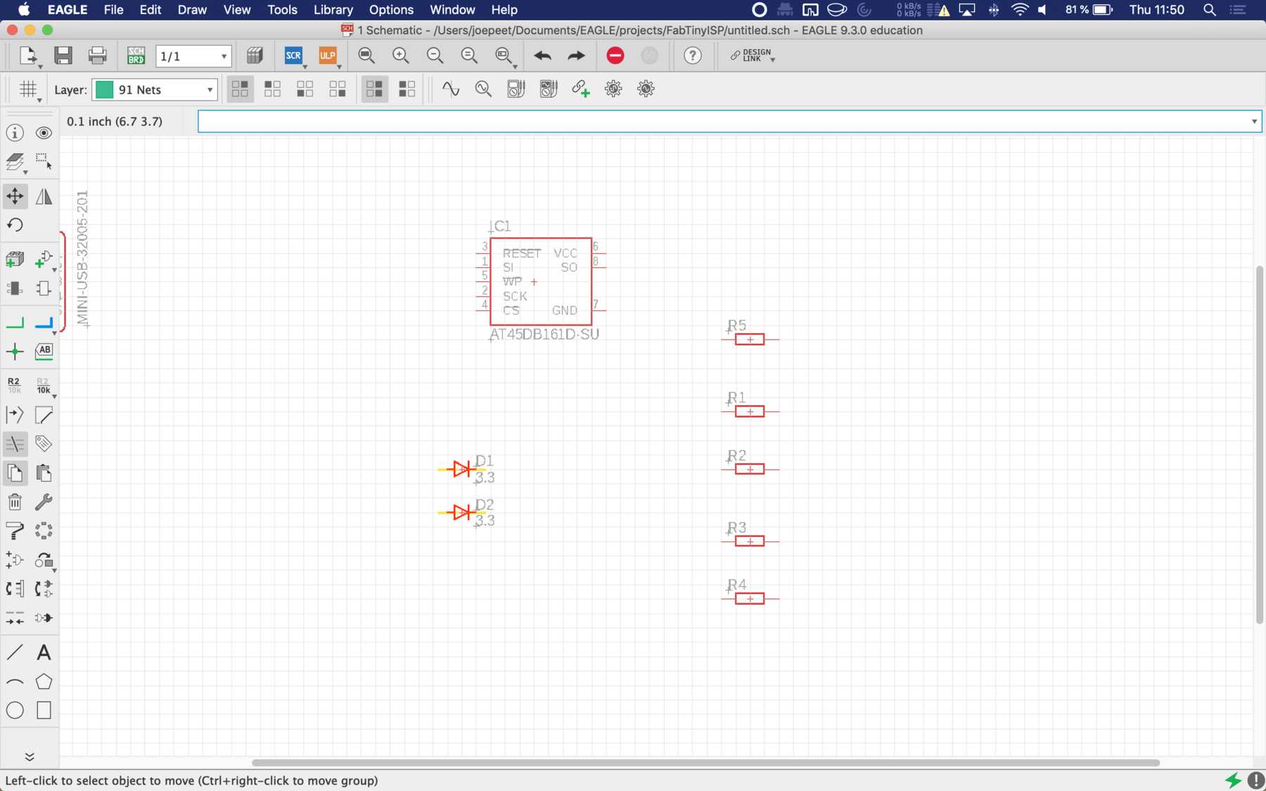
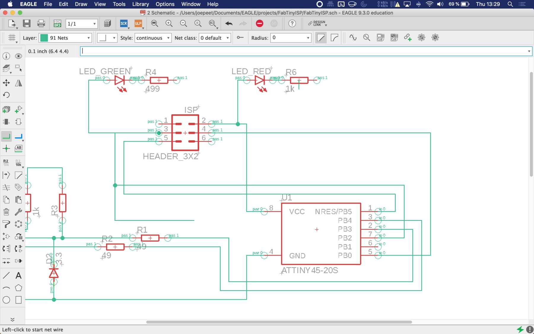
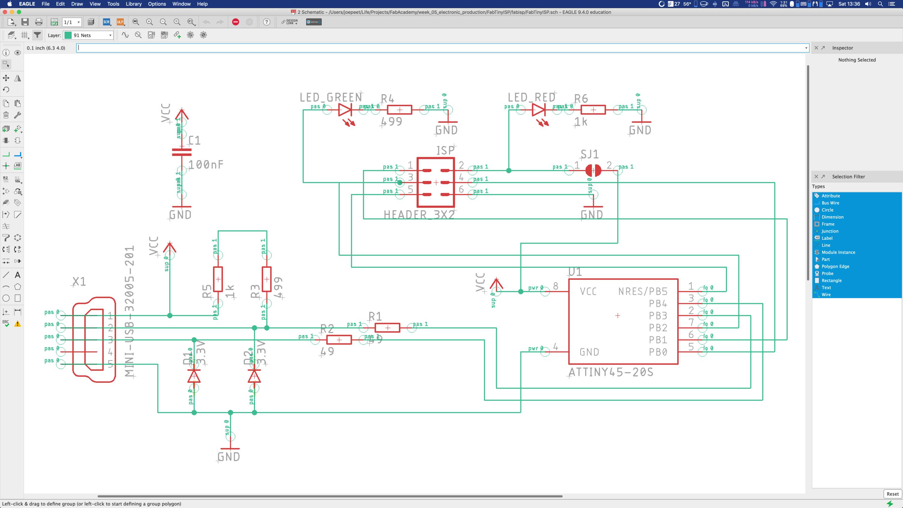
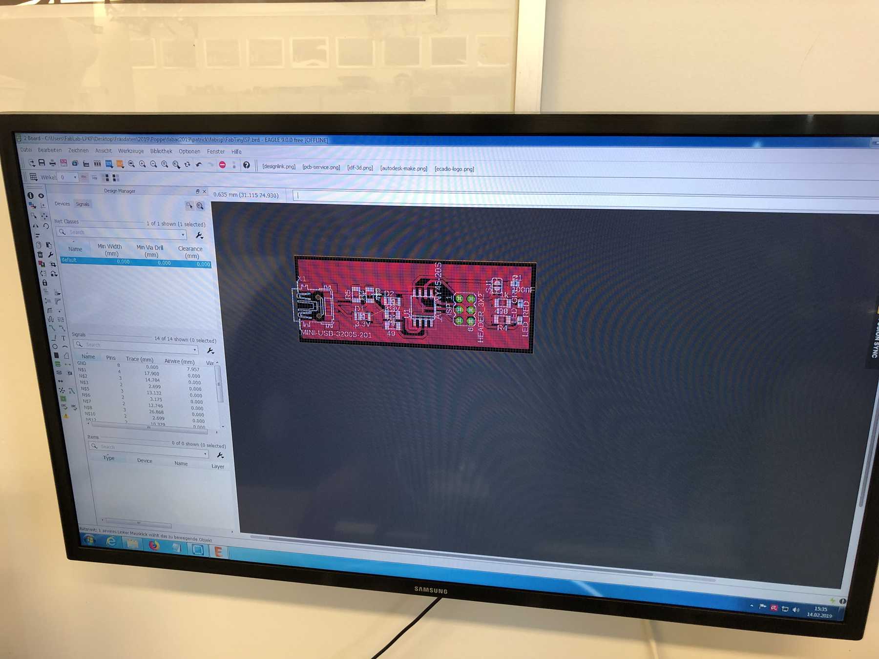
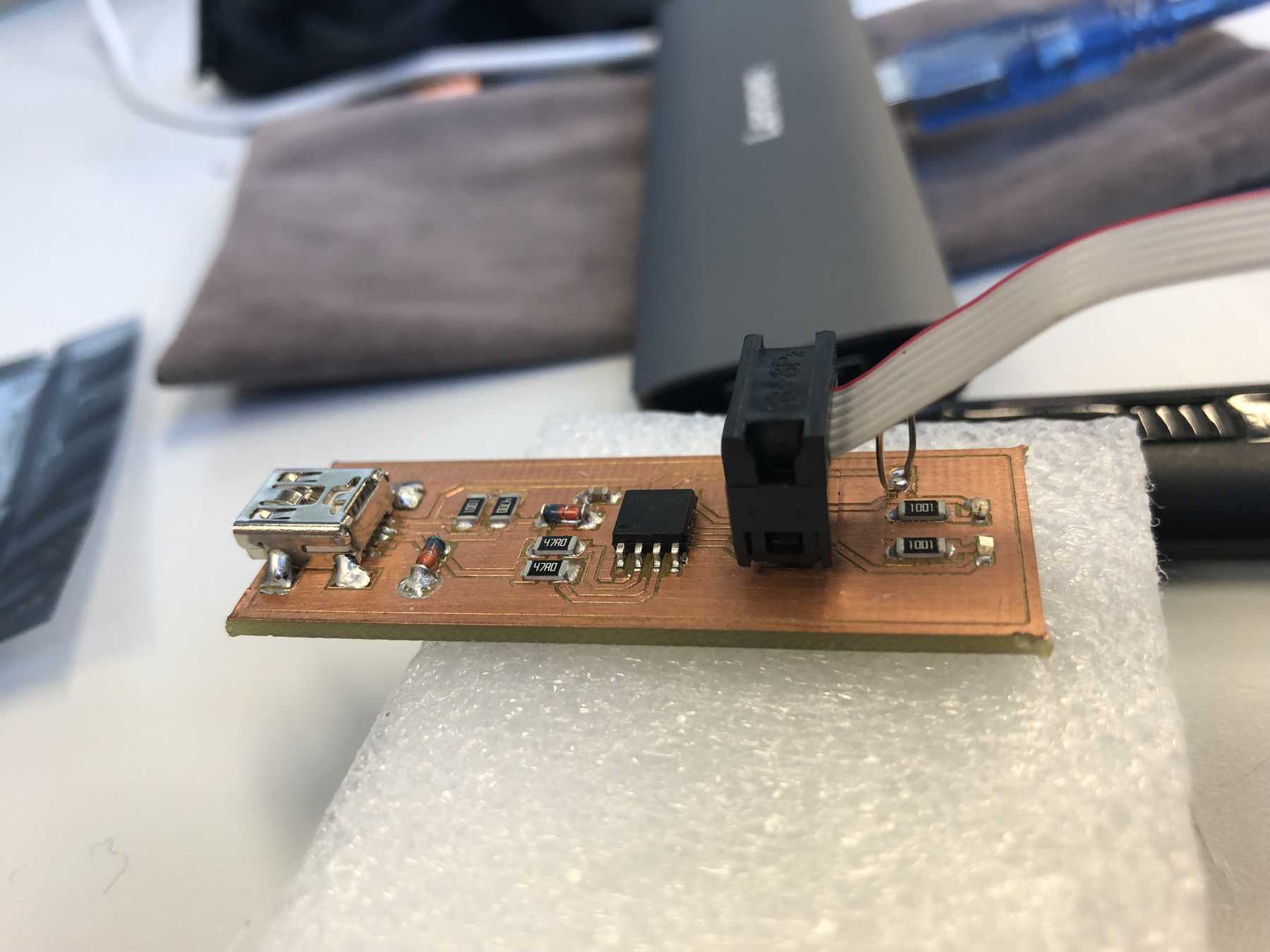
The assignment was to draw a FabTinyISP. I looked into the instructions of Brian and tried to remake his board with some changes depending on the parts we have in our FabLab. Brian’s FabTinyISP is also recommended by Neil, which is due to the fact that the manual is really extensive. The first thing I looked at was his schematic drawing.
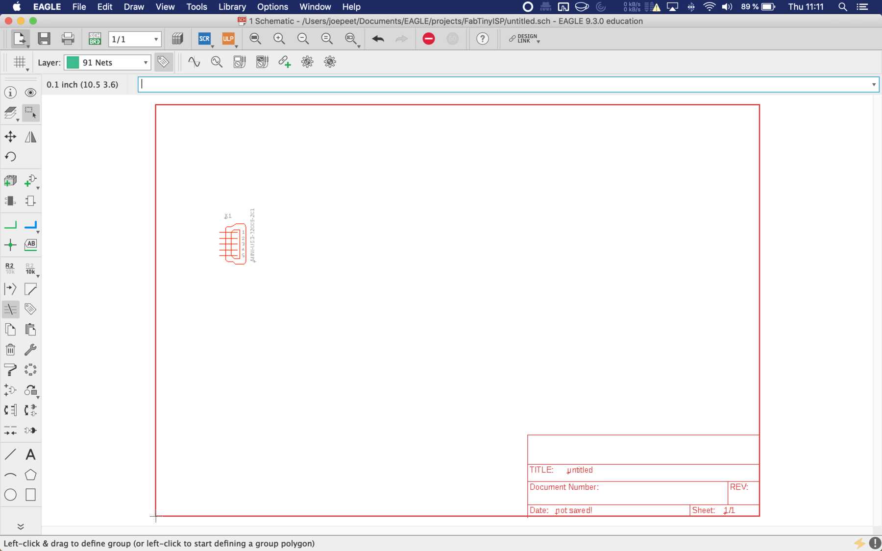
The most important element at the beginning is adding elements. These are added one after the other to the schematic drawing. What you learn here very quickly is how to find the individual components in the program EAGLE. For this, you use the library and have to add more parts if necessary. So I couldn’t find a component for the microprocessor ATTiny 45. Therefore I downloaded the library from the following page and added it. Afterward, I had to connect the individual components with each other and made sure that they really corresponded to the template. Later it turned out that I could simply download the very extensive Fab Academy Library for EAGLE.
I have drawn the board step by step, which can be seen in the following pictures. If a component is not available, you can create the footprint etc. yourself. Autodesk also has a very good video-tutorial how to create PCB parts in Autodesk EAGLE and how to map Step Models to your Packages in Eagle.
All in all I used the following parts for my assignment.
| Qty | Value | Device | Package | Parts | Description |
|---|---|---|---|---|---|
| 2 | LEDCHIP-LED0603 | CHIP-LED0603 | LED_GREEN, LED_RED | LED | |
| 1 | SJ | SJ | SJ1 | SMD solder JUMPER | |
| 1 | 100nF | C-EUC0603 | C0603 | C1 | CAPACITOR, European symbol |
| 2 | 1k | R-EU_R1206 | R1206 | R5, R6 | RESISTOR, European symbol |
| 2 | 3.3V | DIODE-MINIMELF | MINIMELF | D1, D2 | DIODE |
| 2 | 49 | R-EU_R1206 | R1206 | R1, R2 | RESISTOR, European symbol |
| 2 | 499 | R-EU_R1206 | R1206 | R3, R4 | RESISTOR, European symbol |
| 1 | ATTINY45-20S | ATTINY45-20S | SOIC8_EIAJ_208MIL | U1 | ATMEL ATtiny 45 |
| 1 | ISP | MA03-2 | MA03-2 | HEADER_3X2 | PIN HEADER |
| 1 | MINI-USB-32005-201 | MINI-USB-32005-201 | 32005-201 | X1 | MINI USB-B Conector |
The finished schematic drawing then looked like this:
Group assignment
EAGLE - board design
When the schematic drawing was finished, the board had to be laid out. Here you have to pay much attention to how it is possible, how it works and compare the individual traces.
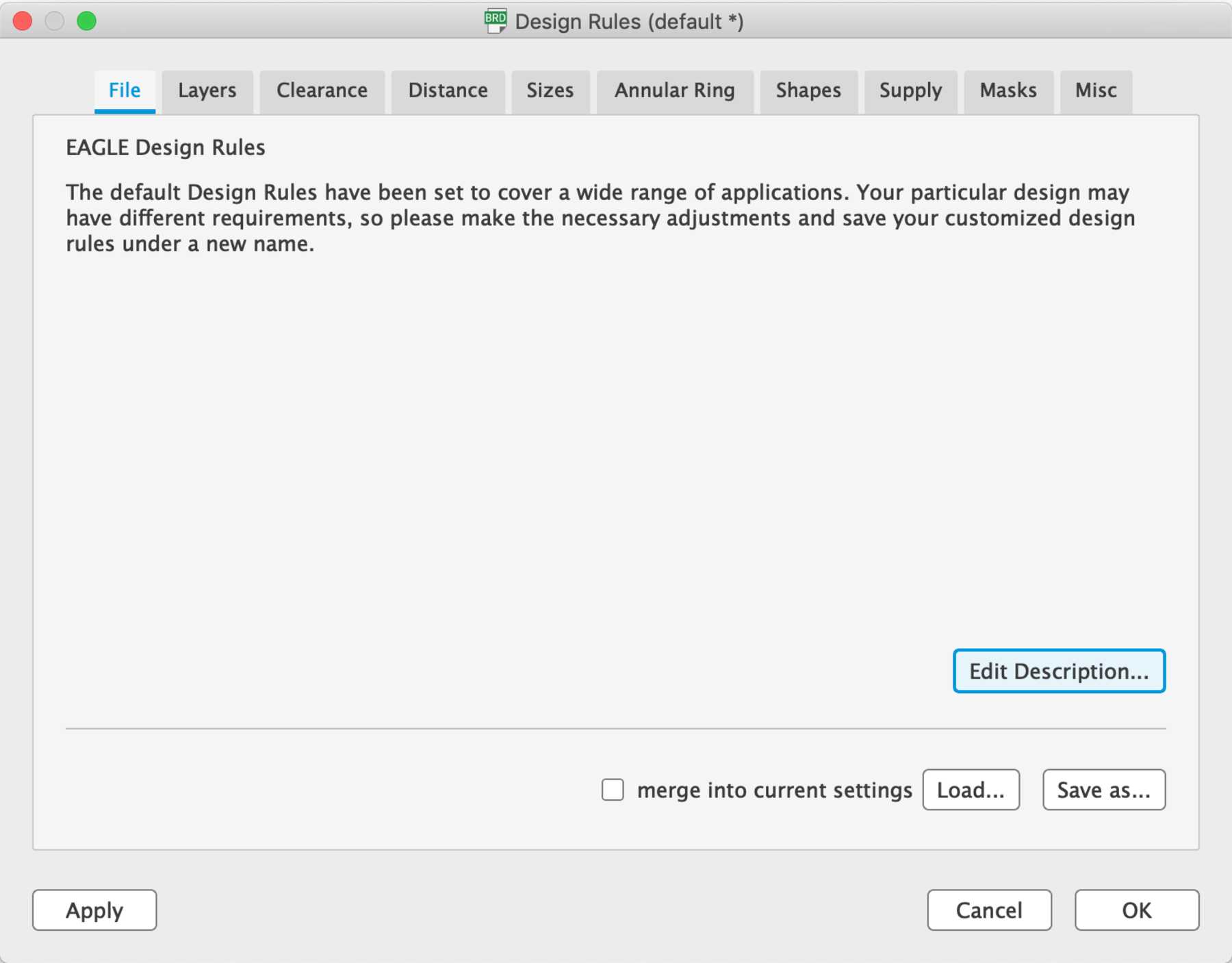
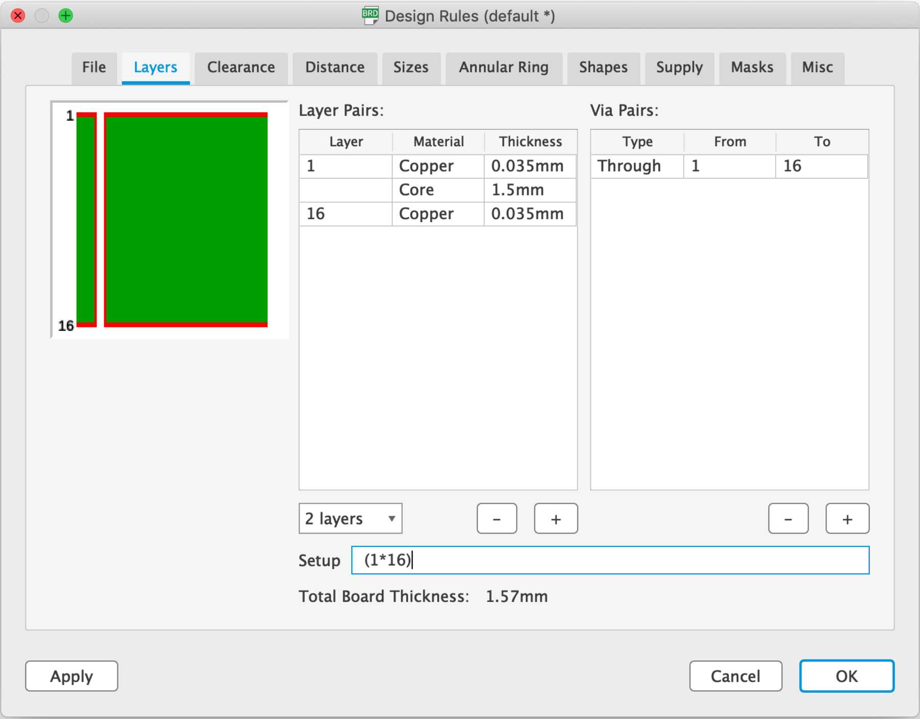
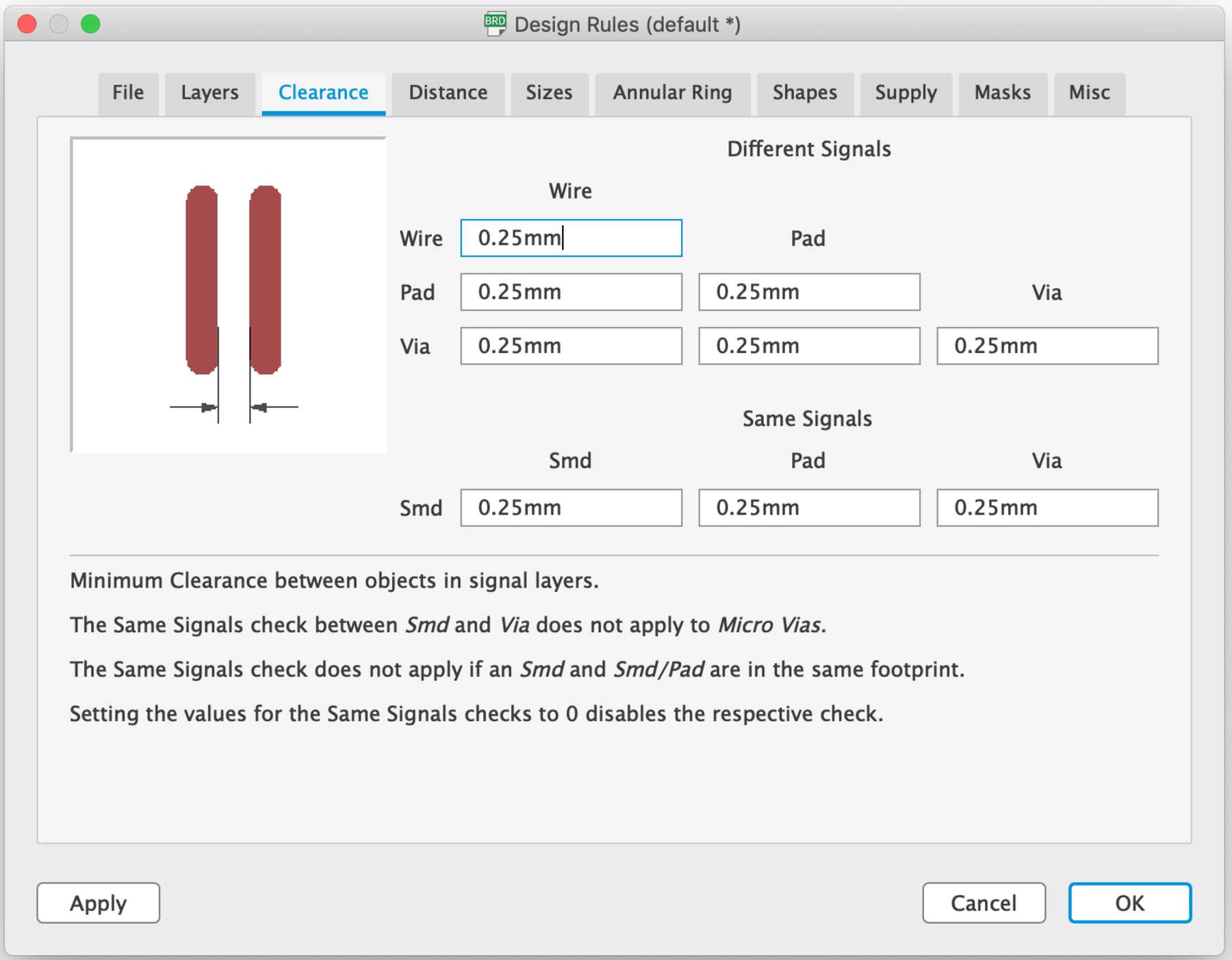
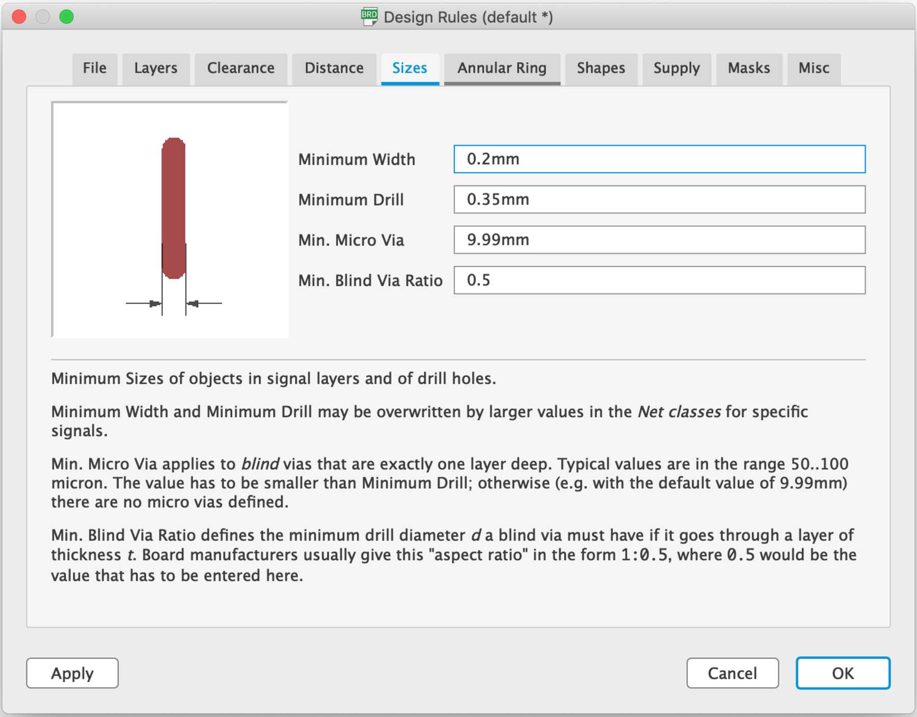
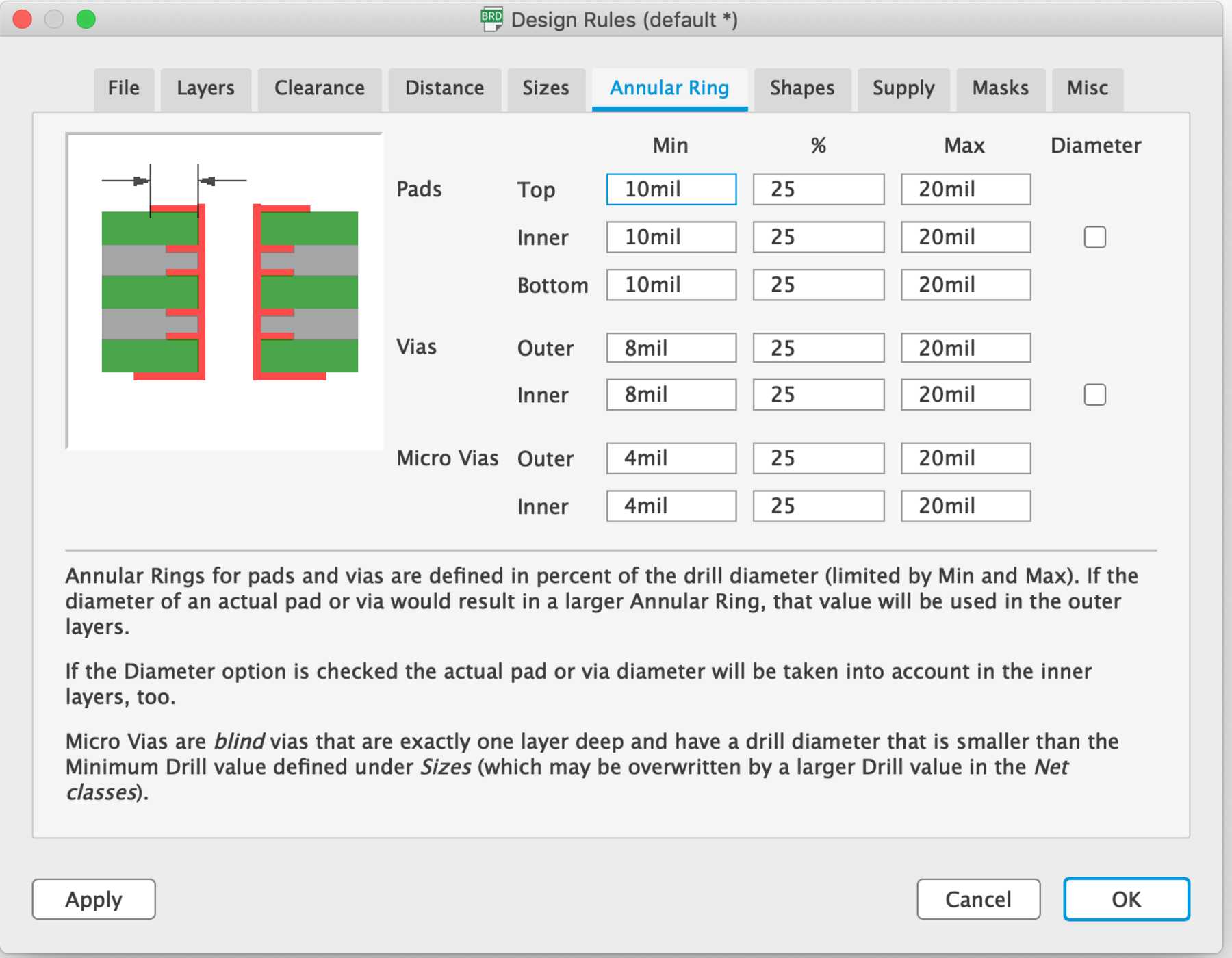
To determine the design rules for EAGLE, especially with regard to the use of the LPKF ProtoMat S63 machine, and for easier application of the smd parts later on. The function for editing the design rules can be found under EAGLE -> Edit -> Design Rules. Here you could set all necessary settings. Our instructor Tobias briefly went through the settings with us, so that we could save them later as a template and use them again and again for further designs.
For example, the distances between different signals were important. This means the distance between wire, pad, via and smd. For this purpose, the program automatically generates different distances in the board design, so that later manual handling is easier or there is no interference. The values can be taken from the following pictures as well as from the attached file at the bottom, which contains the Design Rules of FabLab HRW for easy handling within the Fab Academy.
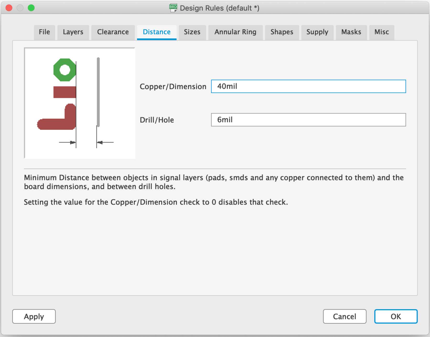
There are several ways for the machine to achieve the desired goal and depending on the distances and, so to speak, the design rules, the CNC machine uses different milling cutters or drills. The LPKF machine has an automatic tool change, which works really well, and an excellent autobed leveling. Later I also use another, smaller machine, which doesn’t have all the features of the LPKF machine, so I was really excited about the capabilities and the milling result of this machine.
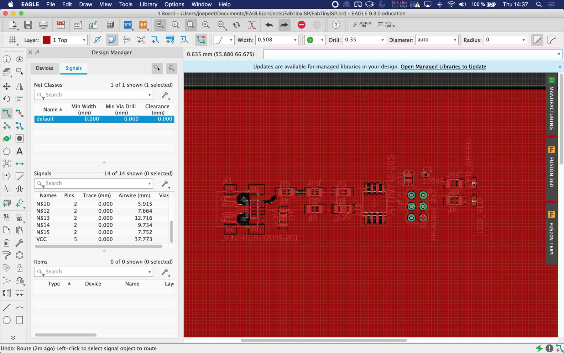
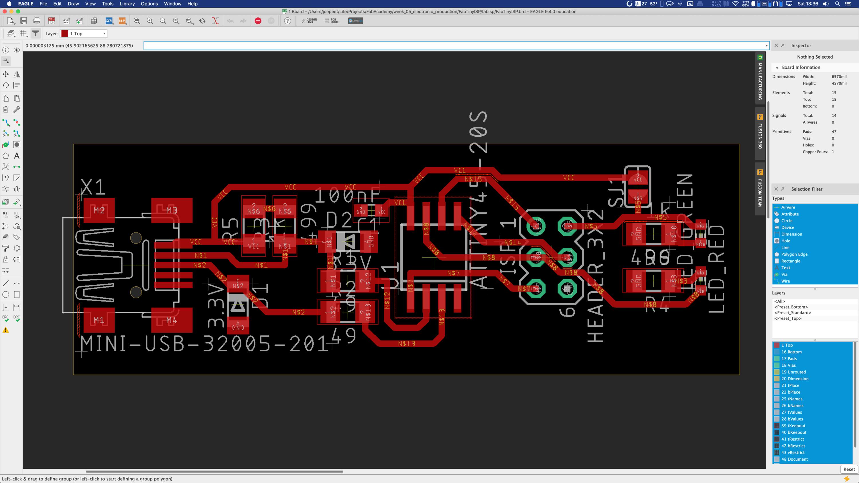
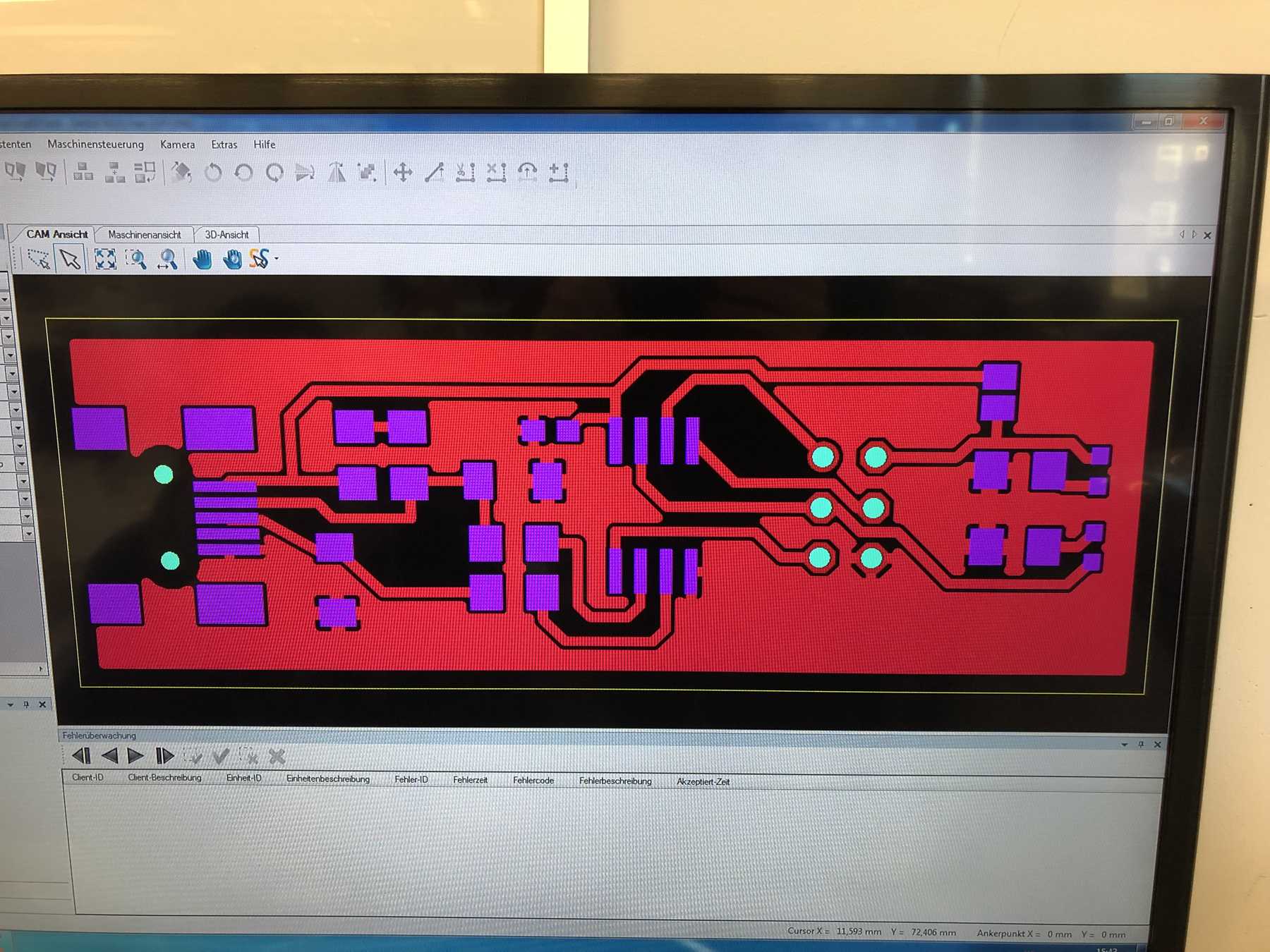
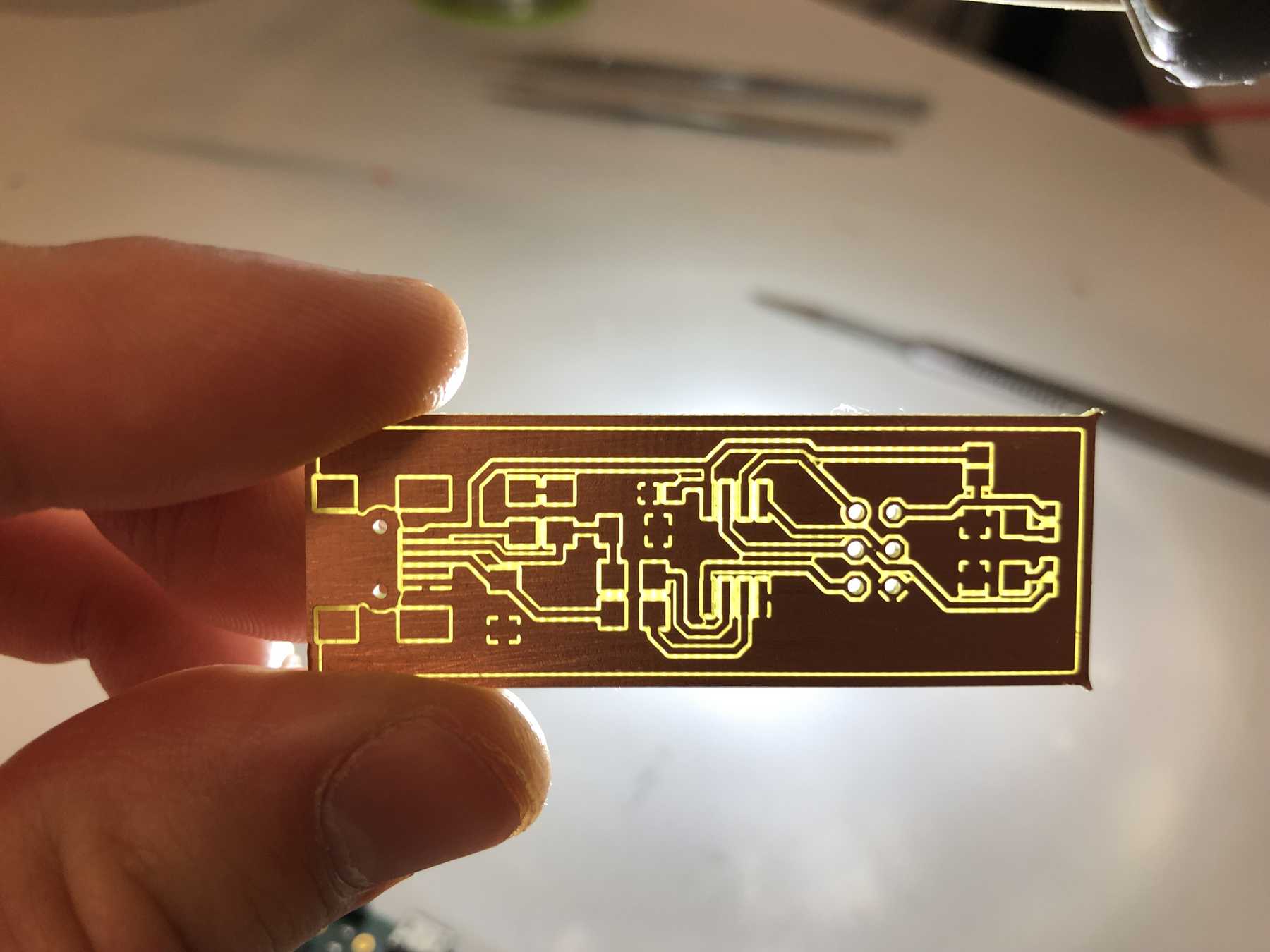
Next, I had to make the design more compact for the milling machine. I reduced the size of the outer lines and then checked again to see if there were any mistakes in the design. At the end my board was designed like this:
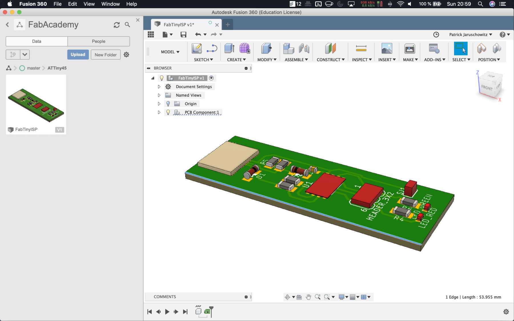
It’s possible to export the pcb design directly to Autodesk Fusion 360 and create a case or something for the board. Here a small impression of the function:
Individual assignment
PCB production
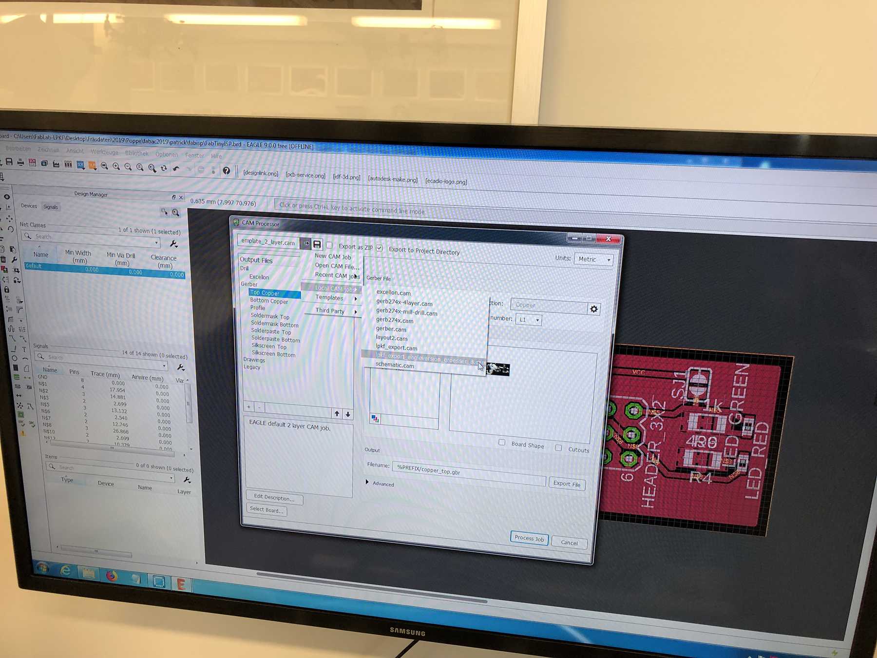
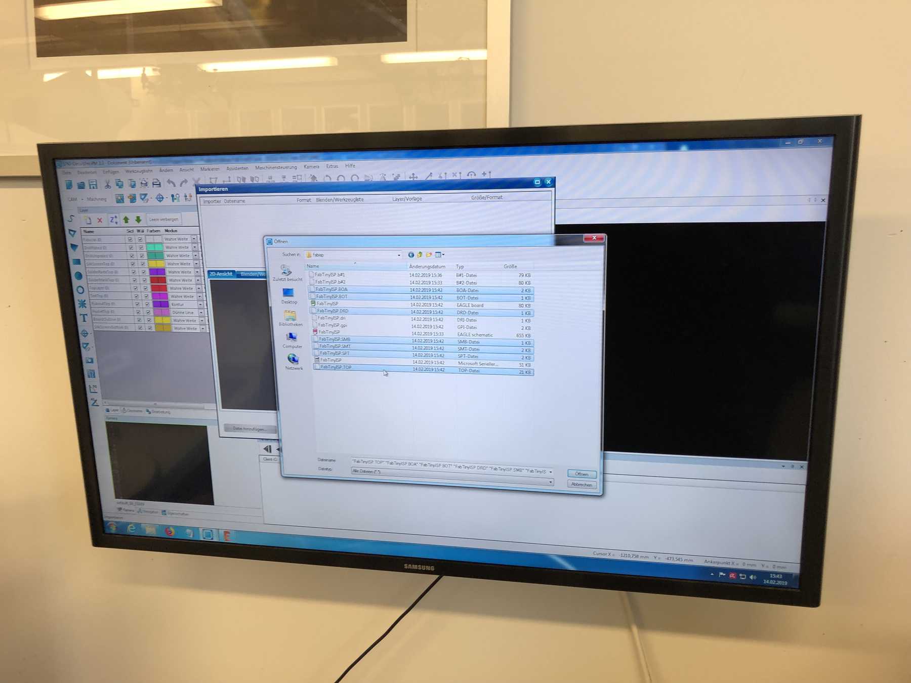
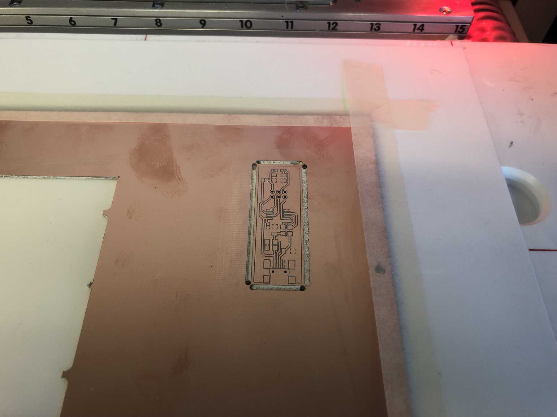
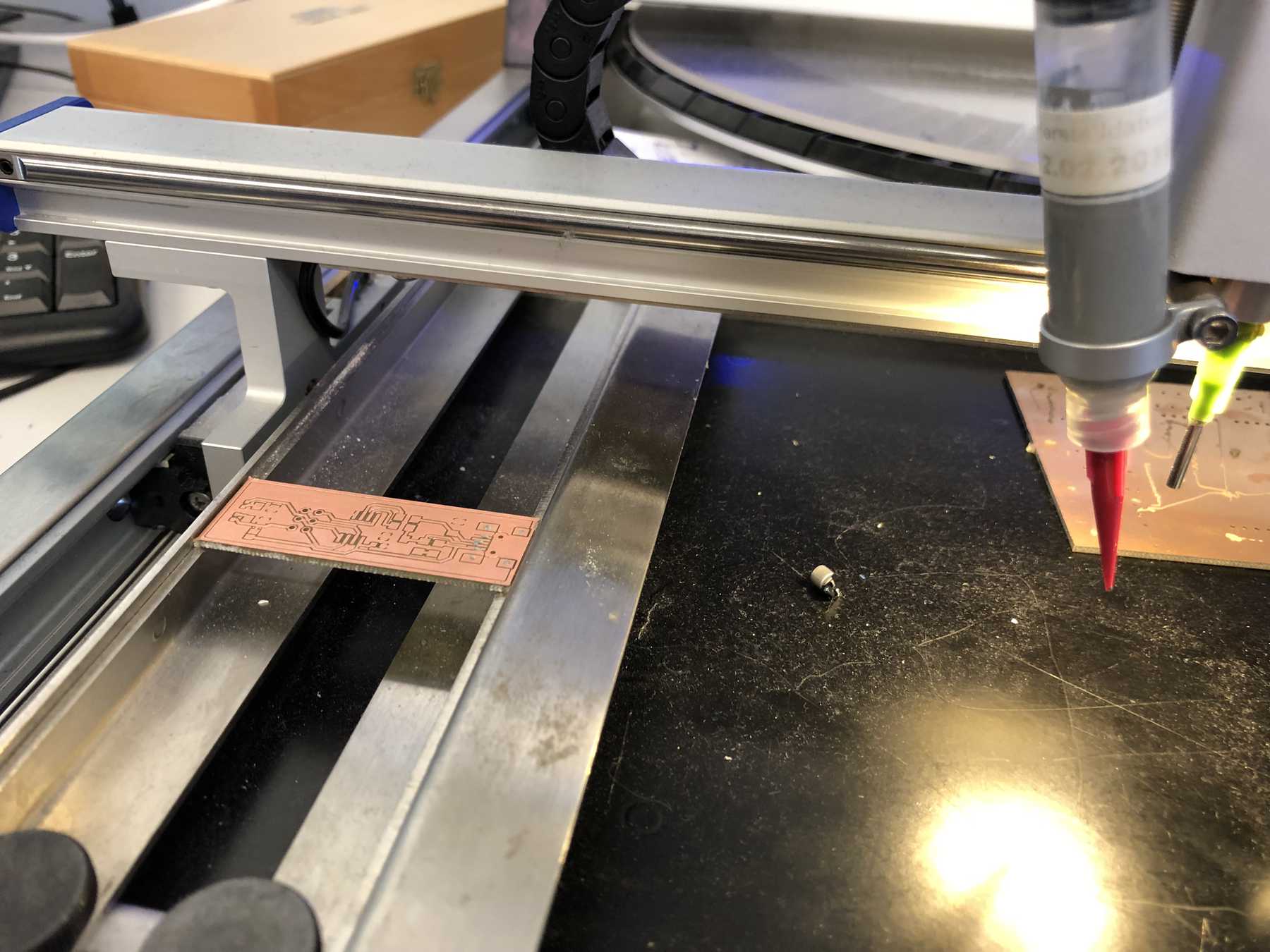
Then we transferred the design via Cam Export with the default settings. When importing into the LPKF program, it was important to us that we only import the Gerber data. This can be recognized by the fact that the endings are all capitalized. In the software itself, I was able to check before the milling process whether everything could be removed from the material as far as I had imagined.
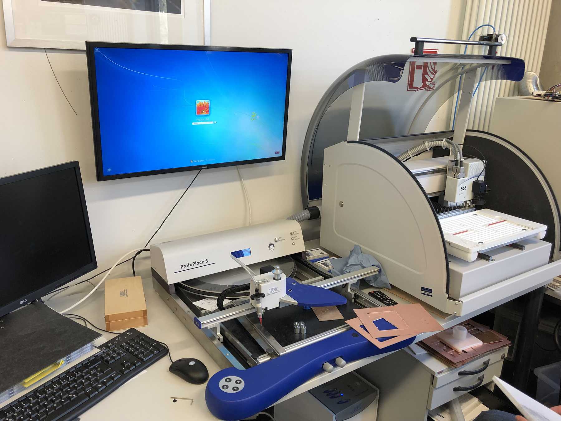
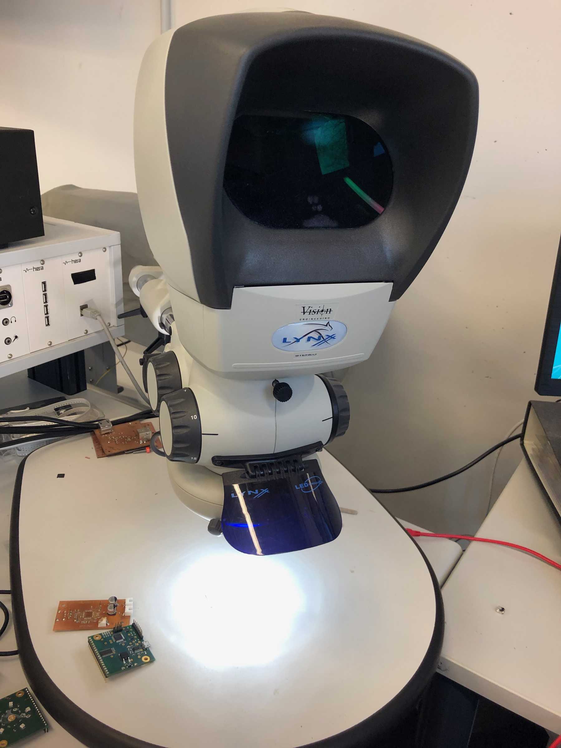
The LPKF ProtoMat S63, which I used, is a 2.5-dimensional machine for any in-house prototyping. It has a high speed spindle with around 60.000 rpm, a fine resolution with 0.5 µm and, thats LPKF says, a great repeatability with +/-0.001mm. It has a camera included and comes with a lot of features. Threw the whole production process it was really quiet compared to the other small CNC-machines I know like the Carbide 3D Nomad 883 Pro. One of the reasons for this, of course, is that the machine has a housing.
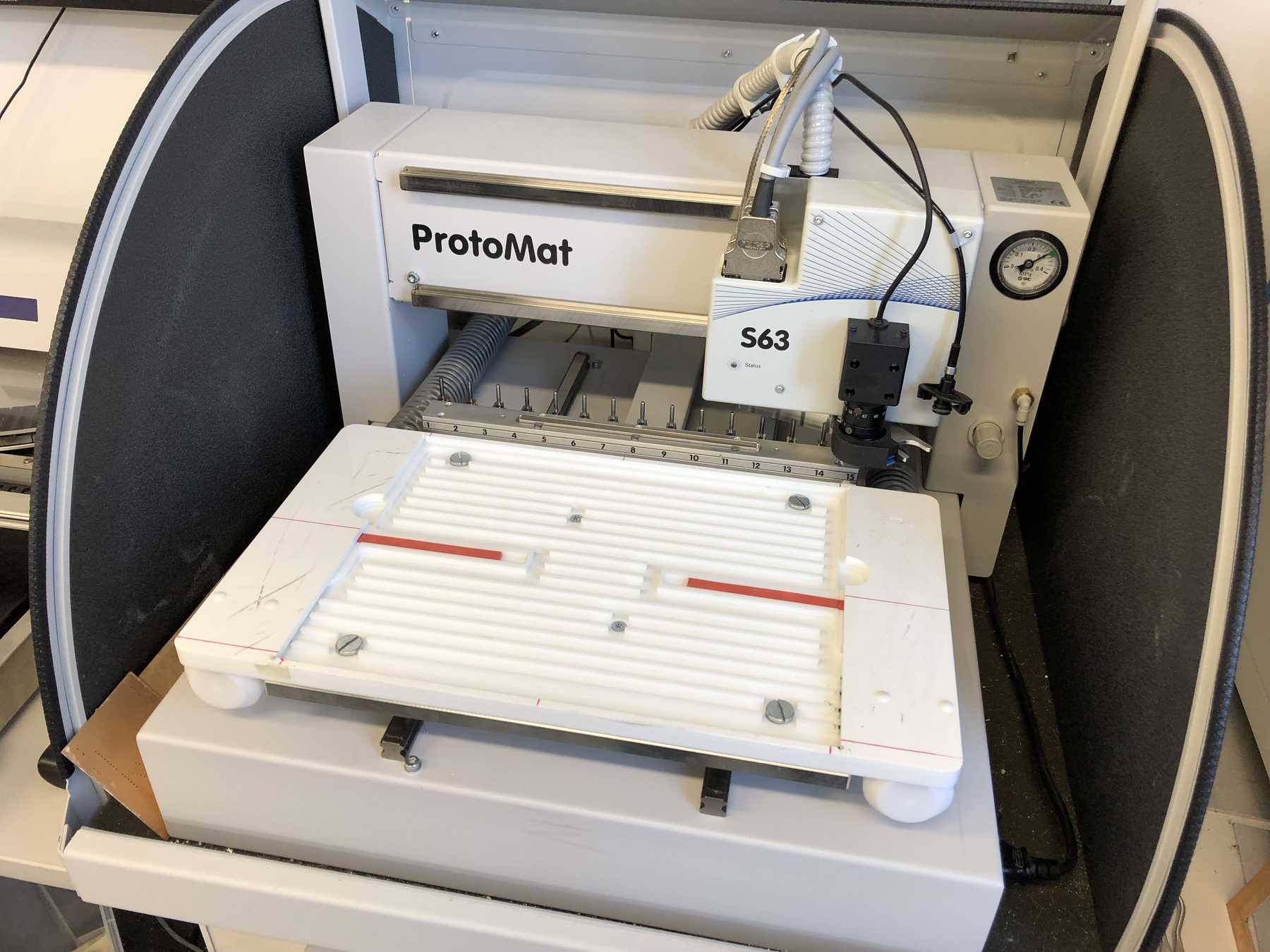
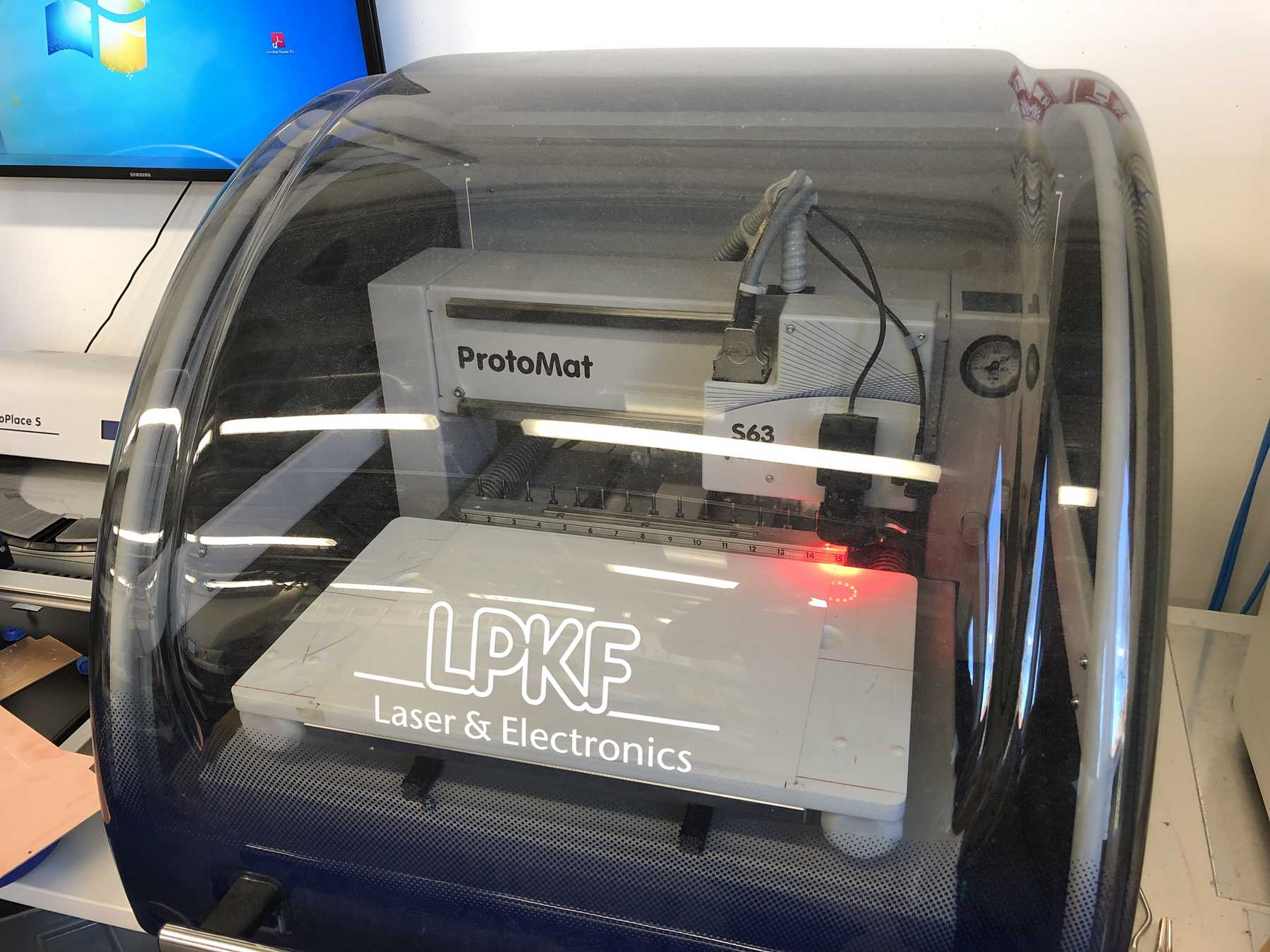
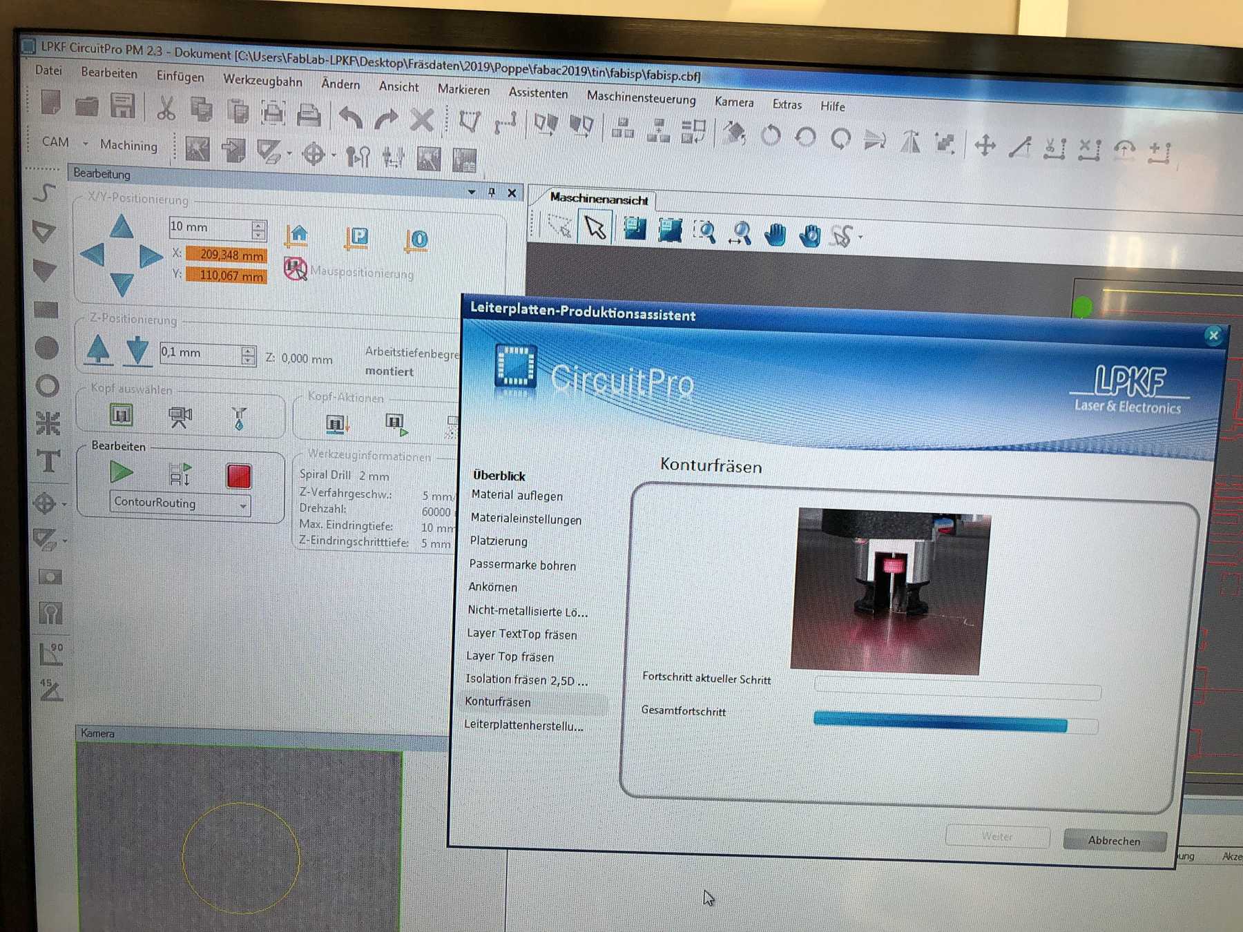
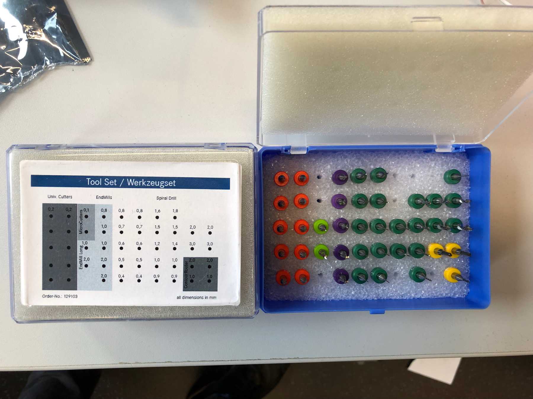
We placed the FR4 material on the vacuum plate and then attached it with adhesive strips. Thus it was secured for us that the board does not move during the individual processes. Then there was a visual inspection for all further steps and afterwards the machine carried out most of the steps itself - which I was really enthusiastic about, as often mentioned. The Autobedleveling, the automatically toolchange during production with up to 15 tools, compared to many other machines, I was raved about every time I used them.
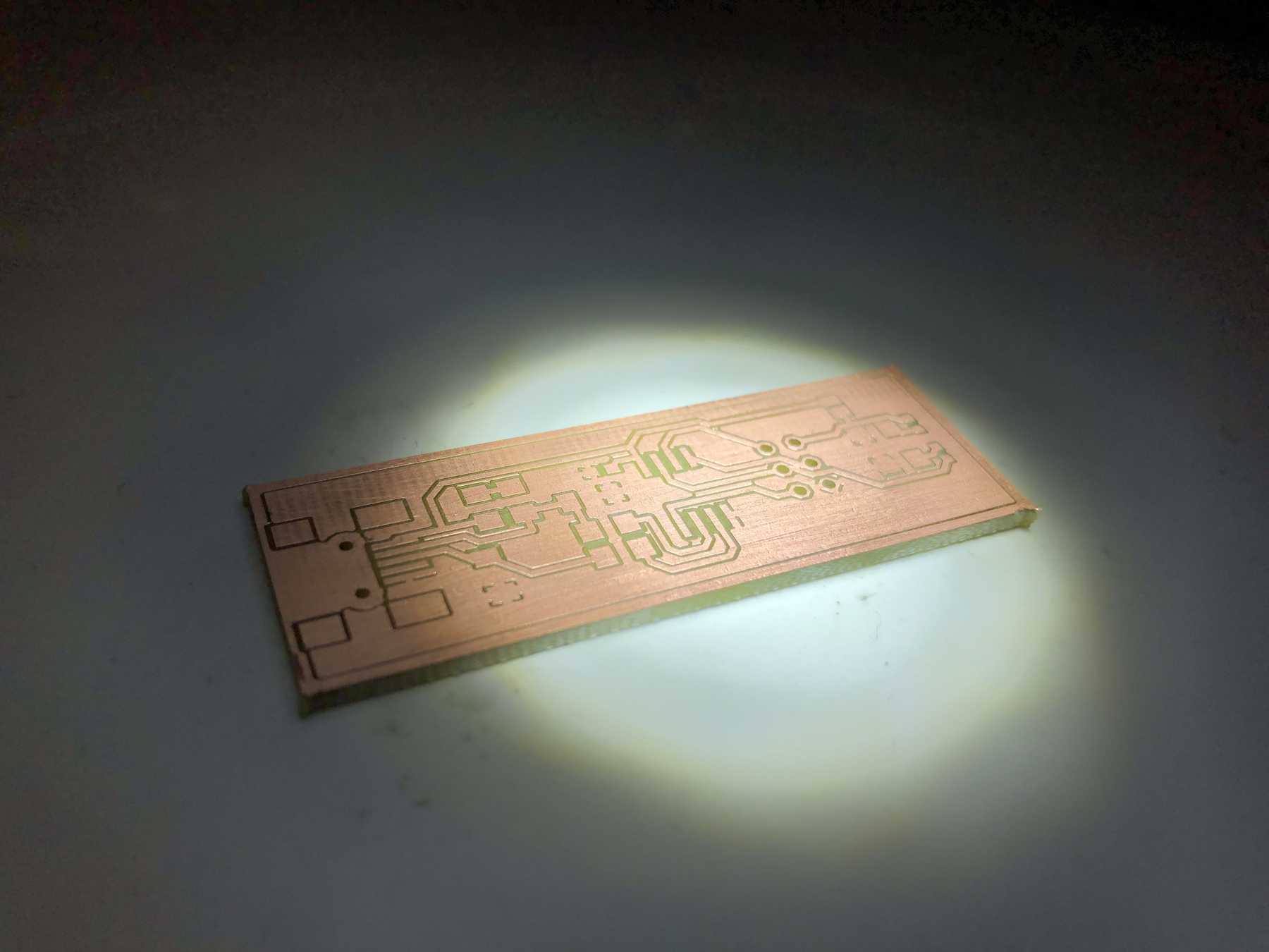
In the end, the milling process consists of a few steps. First the whole process was marked with the drill. Then the traces were milled and finally the outer one, so that they can easily be removed.
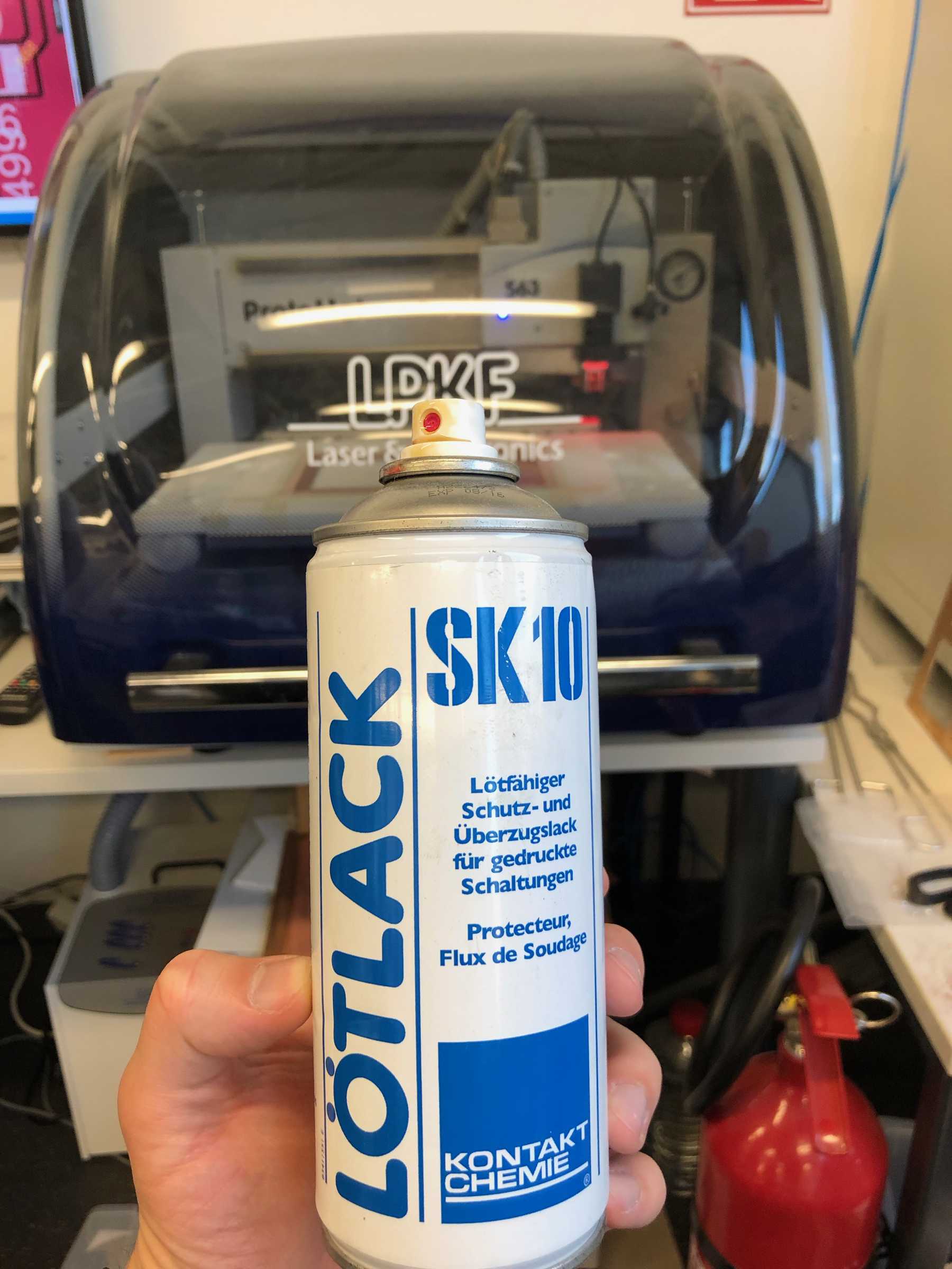
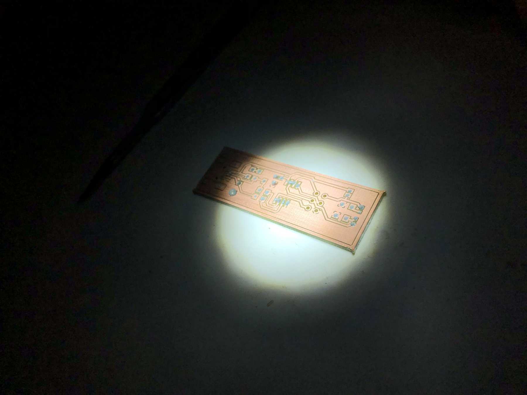
After the production I applied a layer of solder varnish in a distance of 30 cm on the board, which one lets dry afterwards a few minutes in the air. The flux based on natural resins forms a lacquer-like, transparent protective film. This protects printed circuit boards from corrosion and at the same time facilitates further processing. It makes a big difference whether the circuit board was sprayed with solder varnish or not - so this step is highly recommended.
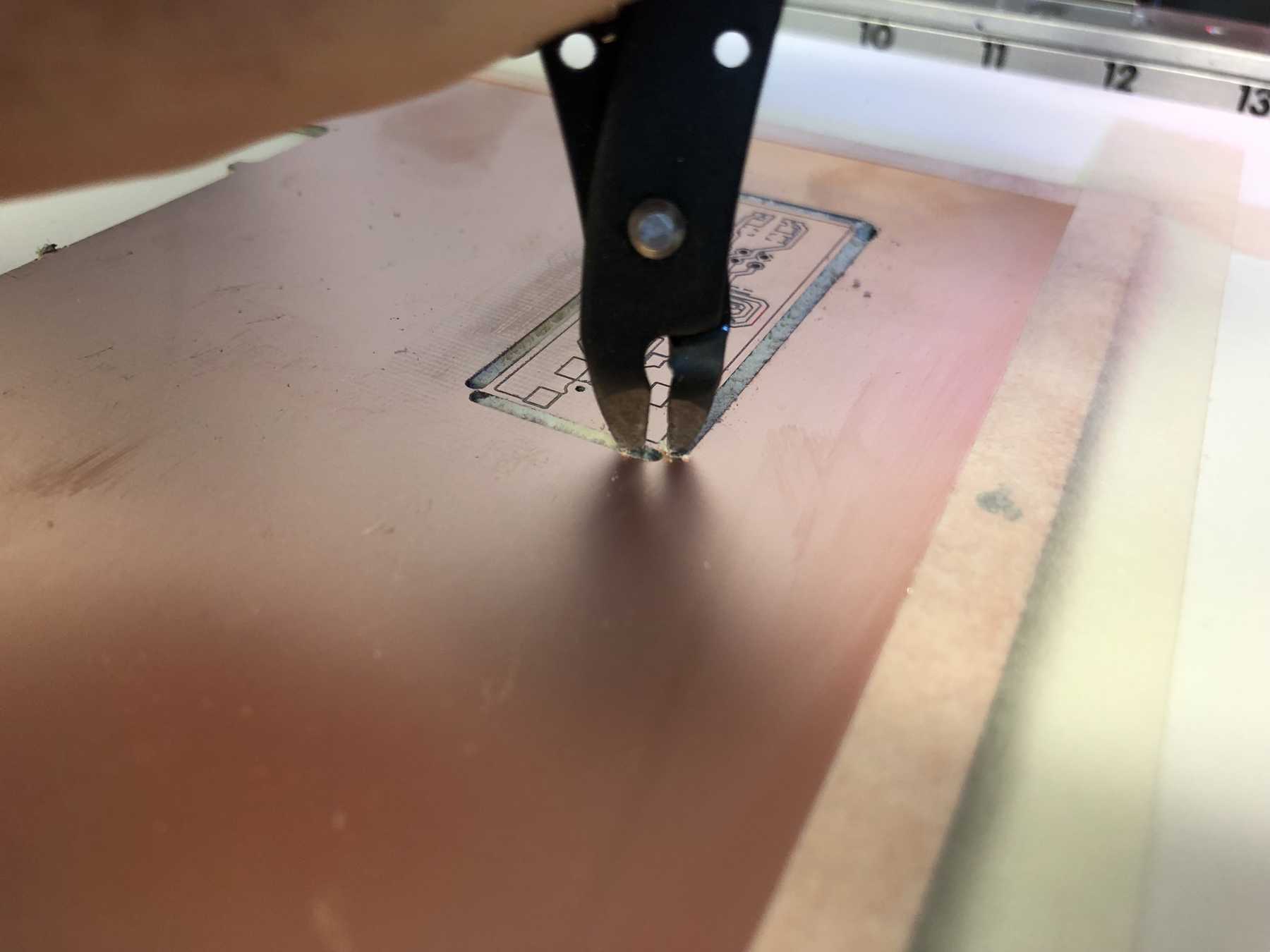
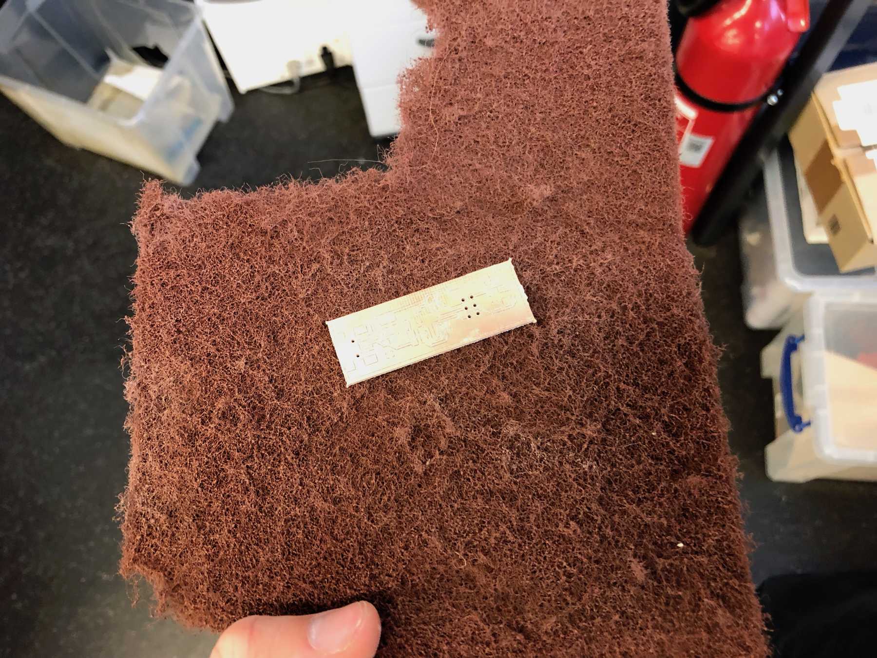
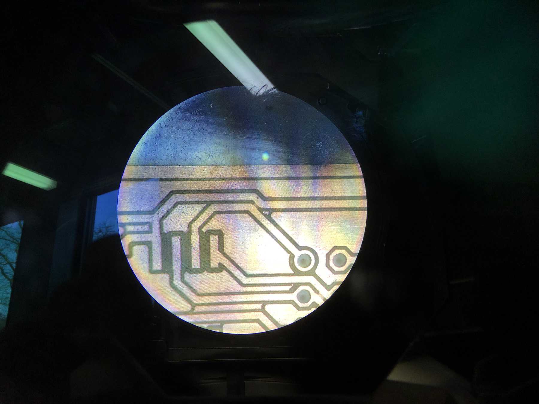
With the help of a 3D microscope I could see that there were still small areas that the machine had not milled cleanly. These were removed with a sharp knife for nursery. At the end, there shouldn’t be any connection anywhere between the traces.
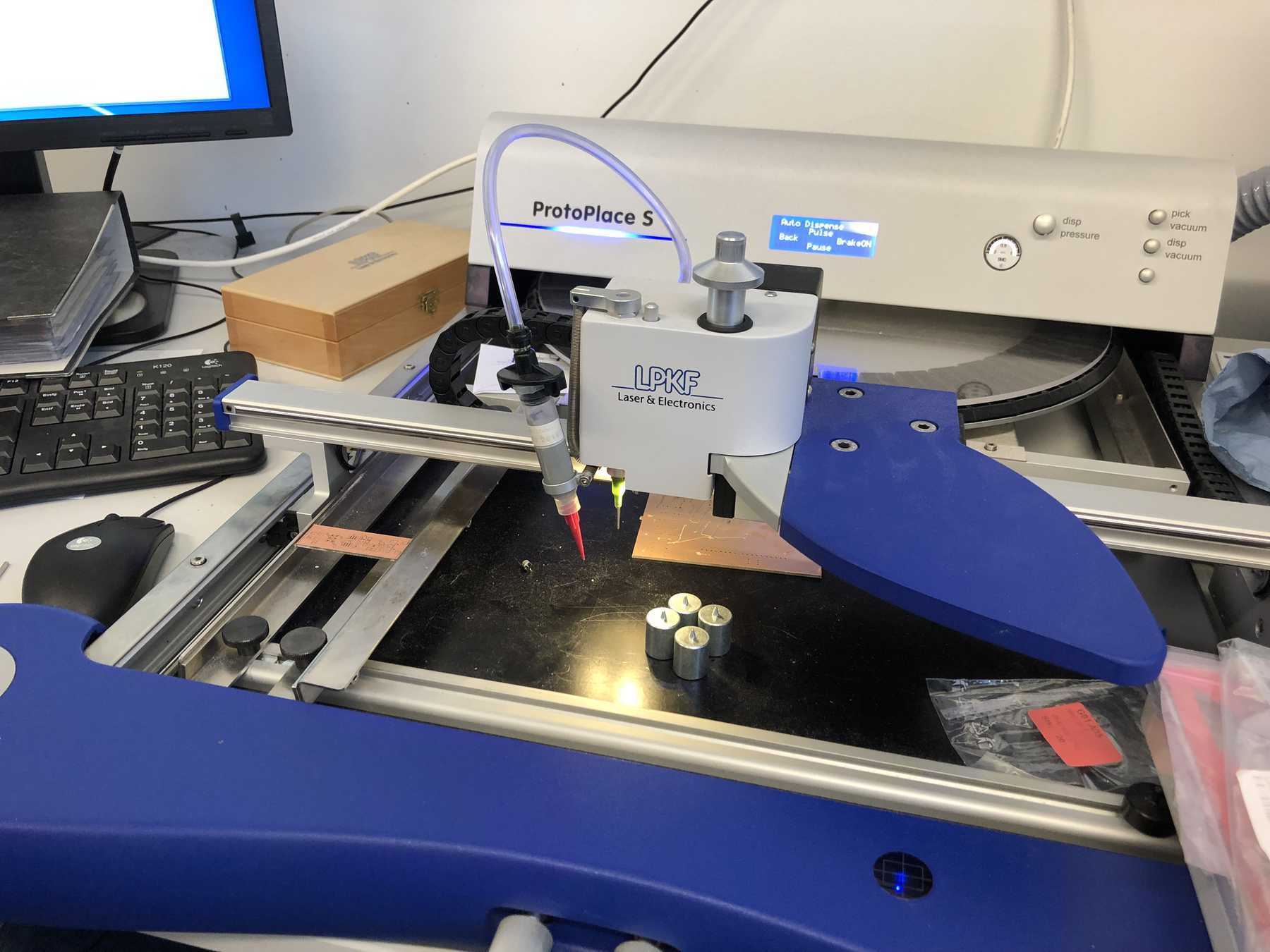
Afterwards the phase could begin with the placement. For this purpose I had to apply solder paste finely. I used the ProtoPlace S, where with the help of compressed air and a foot pedal an always identical, preset amount can be dispensed. This makes it much easier to apply the solder paste to the printed circuit board. Finally I put the components on the PCB with the help of tweezers.
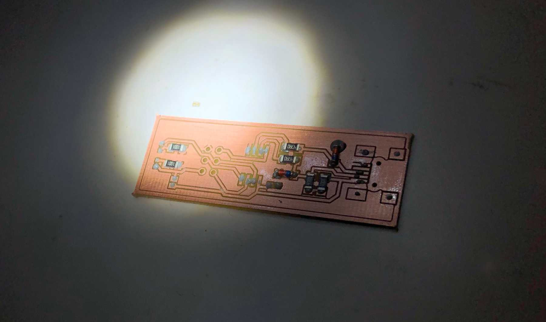
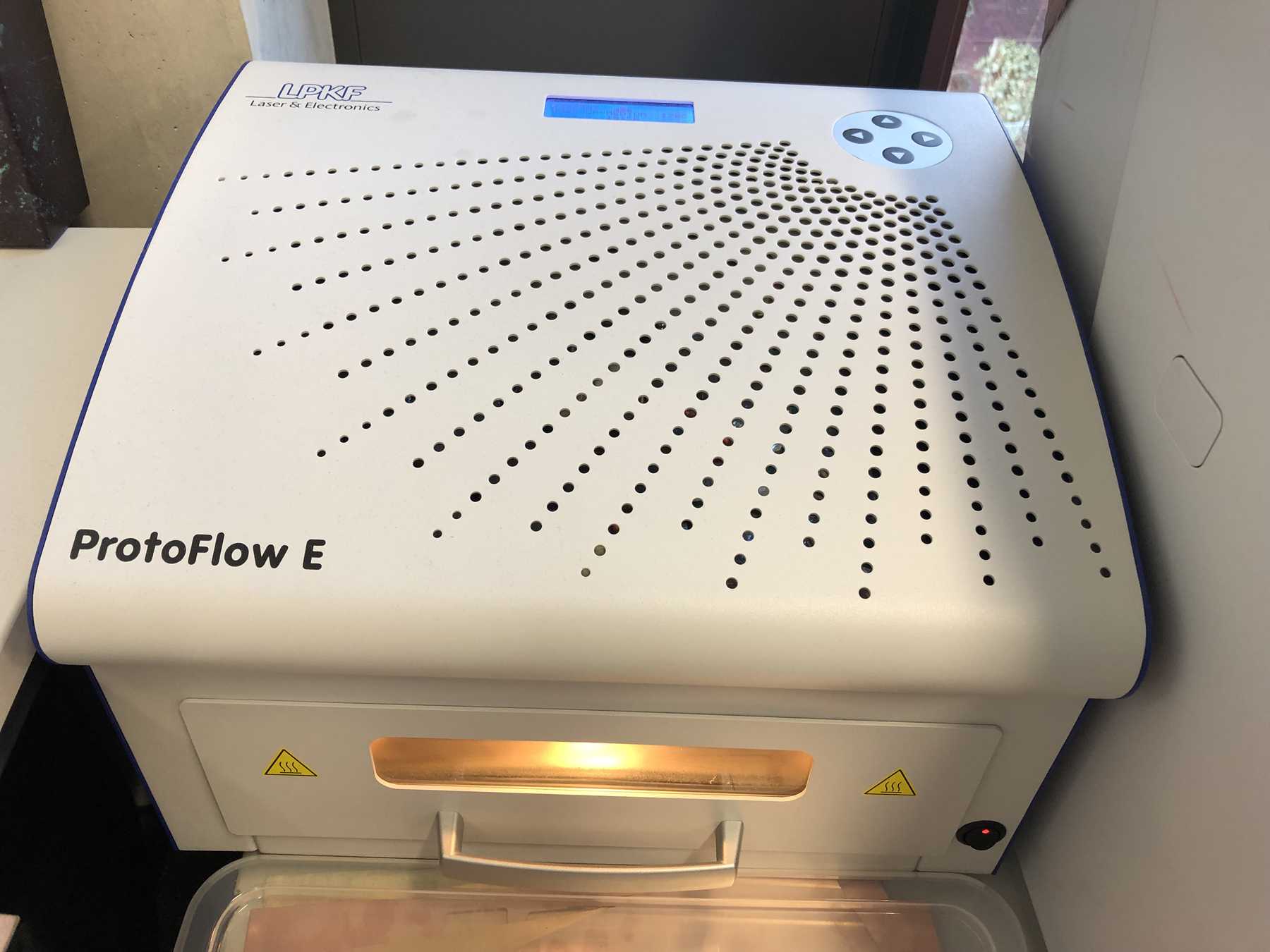
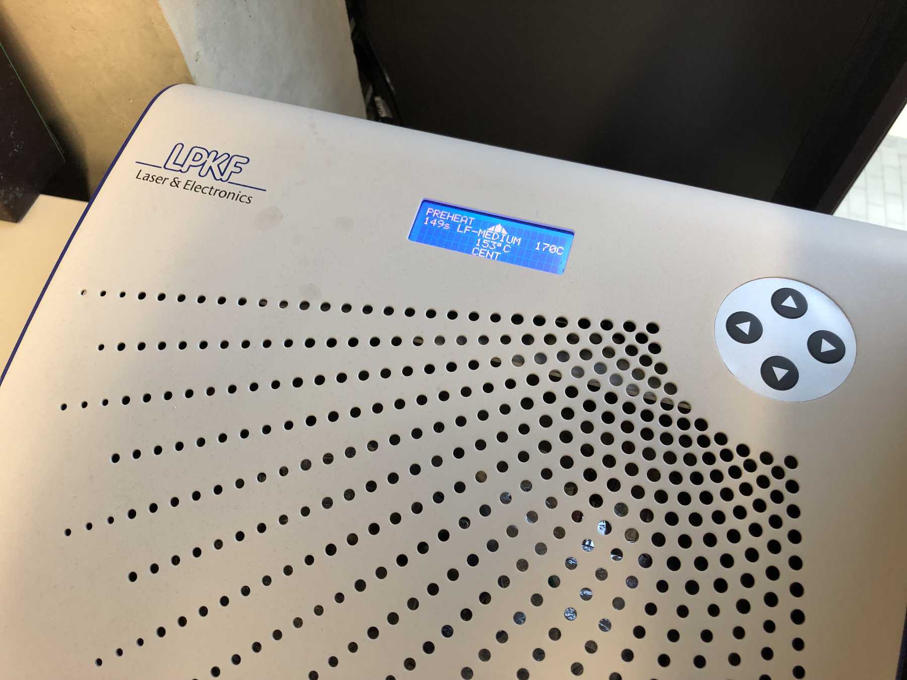
The following reflow process with the parameters and the different heating zones was already deposited, because I also found the LPKF ProtoFlow E before me at the HRW FabLab. Due to the high temperatures of over 250°C, the solder melts out of the solder paste. Due to the surface tension of the molten solder, the components are automatically placed on the pads.
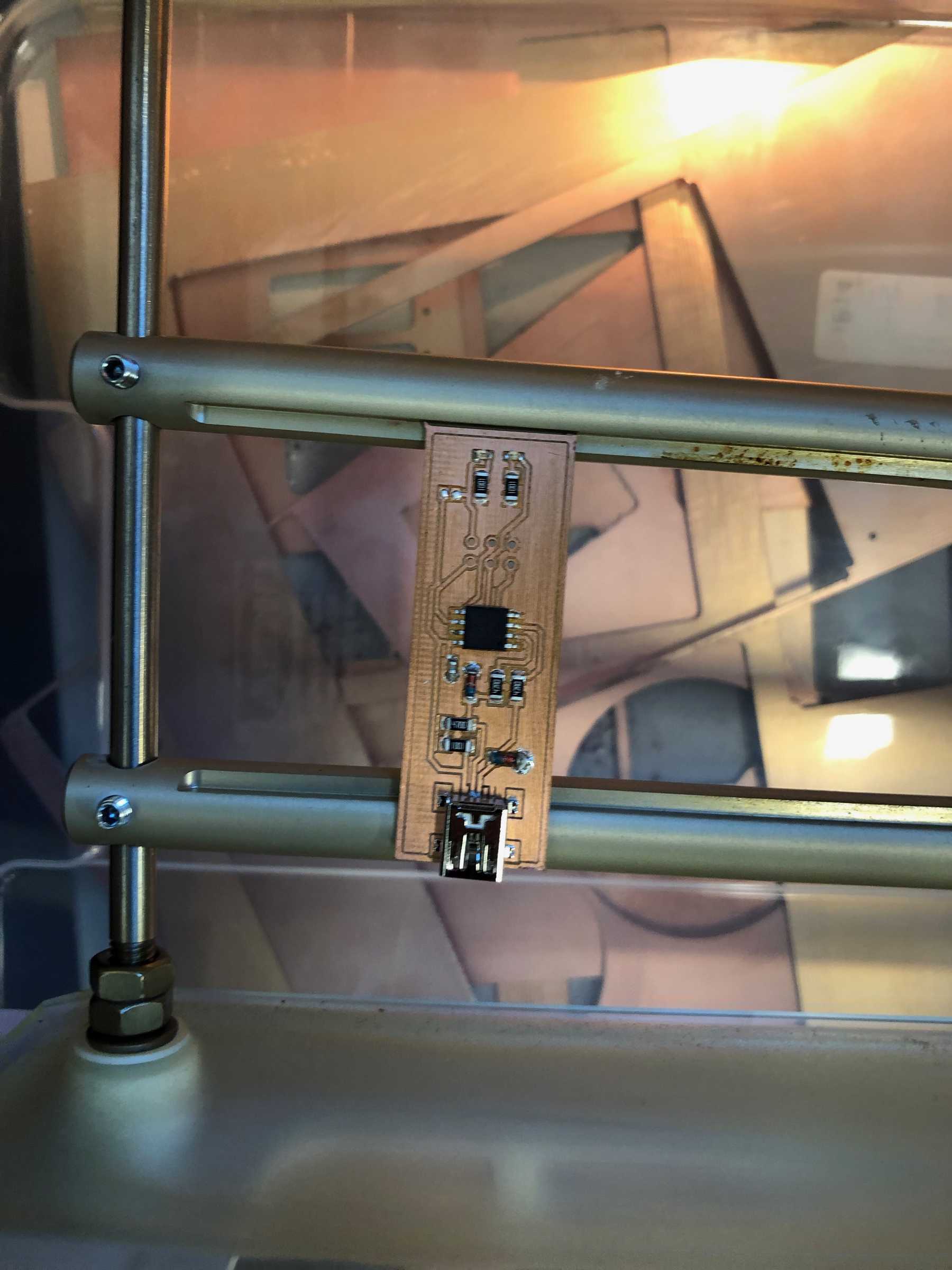
After a few minutes my first board was ready and I was more than a little enthusiastic about this prototype! Later you learn more and more and then you would have changed some things in one place or another, but I was at this moment really satisfied.
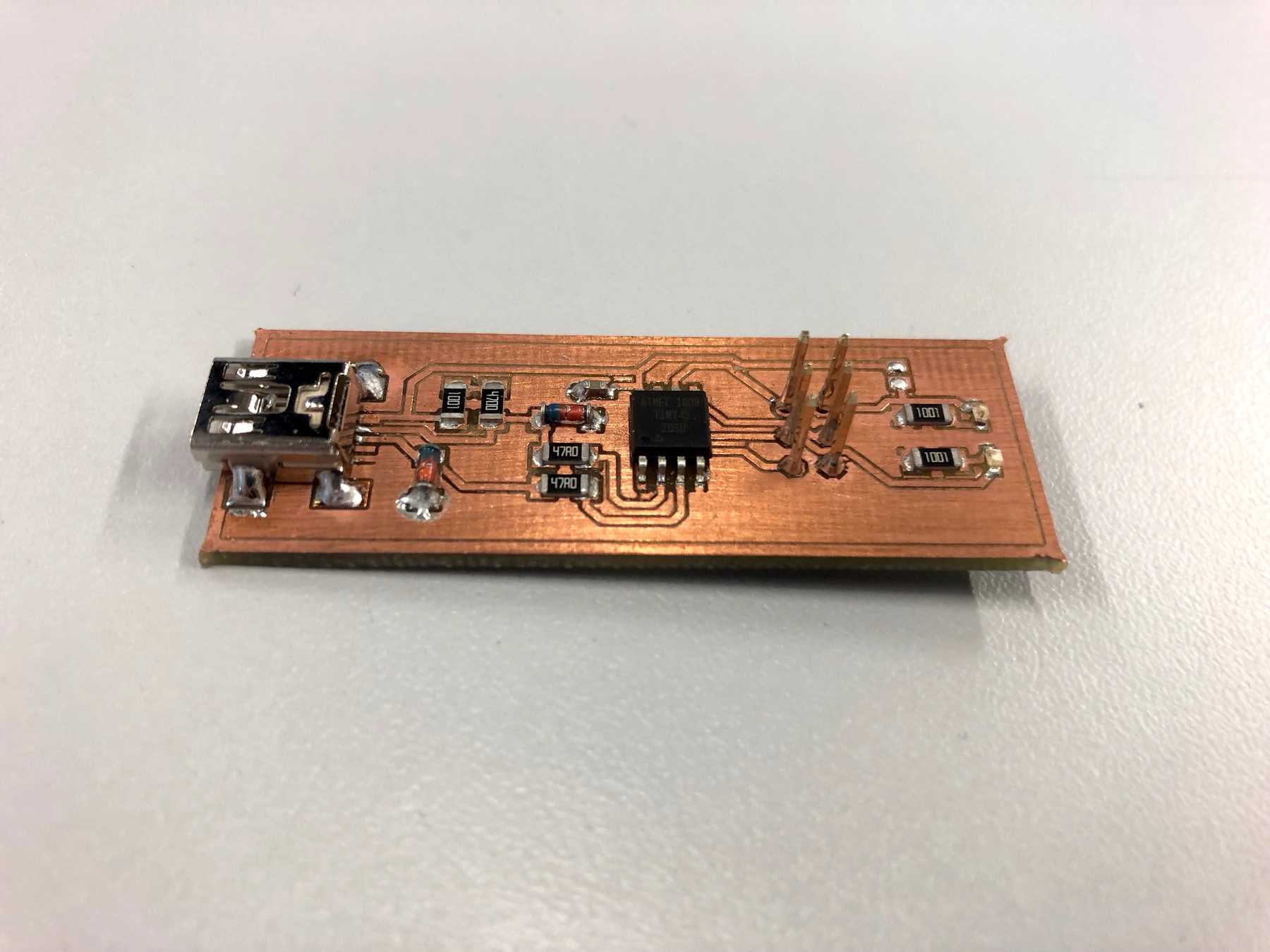
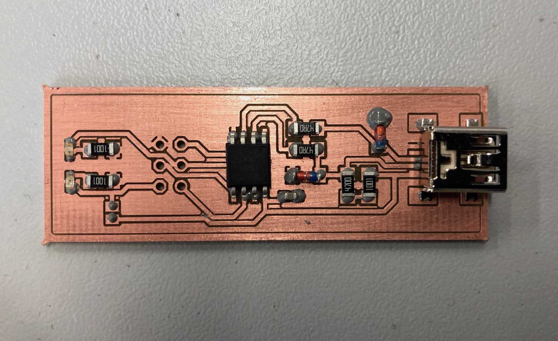
According to Brian it was necessary to connect two more pads with each other - the jumper can be realized by a 0 Ohm resistor or by soldering something on it, which is conductive. Said and done.
With the help of a multimeter I now checked all possible connections, checked if there are any other traces connected to the ground by any parts or not. VCC and GND should not have any connections. But it didn’t seem like it and I was really happy. Next I had to programm the ATtiny45 what to do. For this I used an ISP programmer. Unfortunately, the first one didn’t work so well and I didn’t want to waste too much time, so I didn’t have any problems with the AVRISP programmer of DIAMEX on the Mac. I connected it to my ISP header on my FabTinyISP.
Programming the usbtiny
I installed CrossPack for AVR® Development on my Mac. Later I found out that I should reinstall AVRDUDE - but more about that in week 07.
I downloaded the firmware for the FabTinyISP from here.
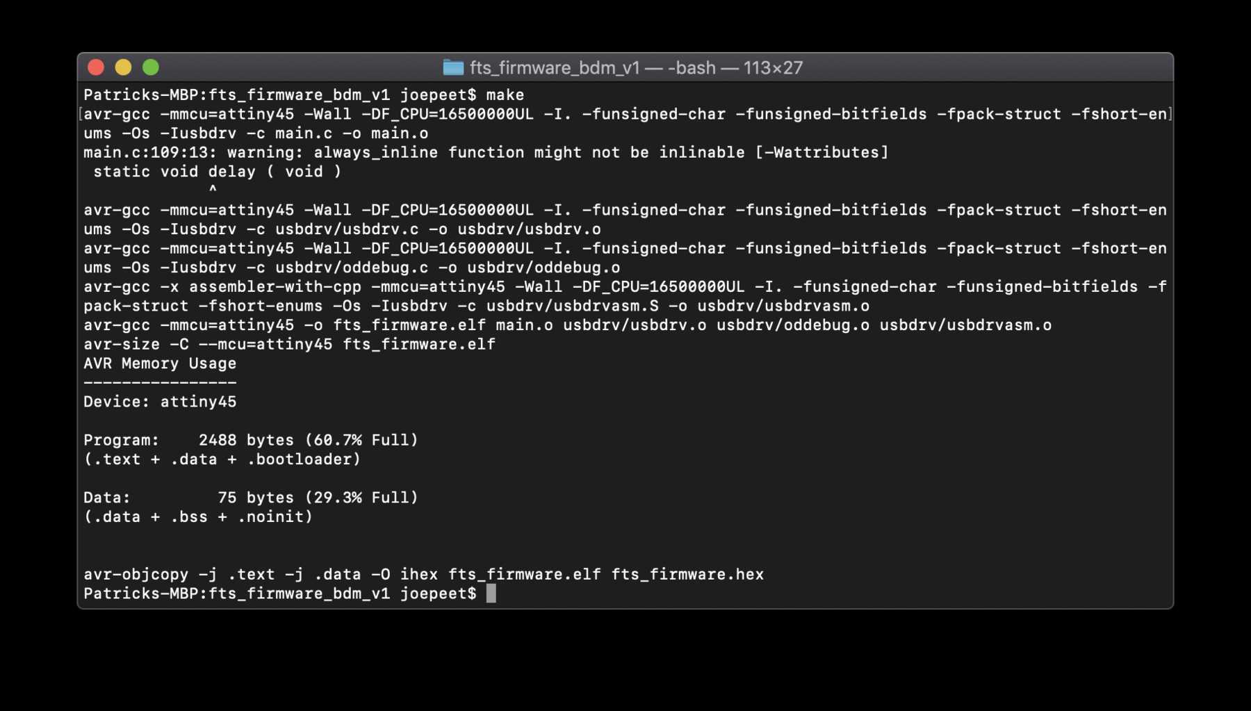
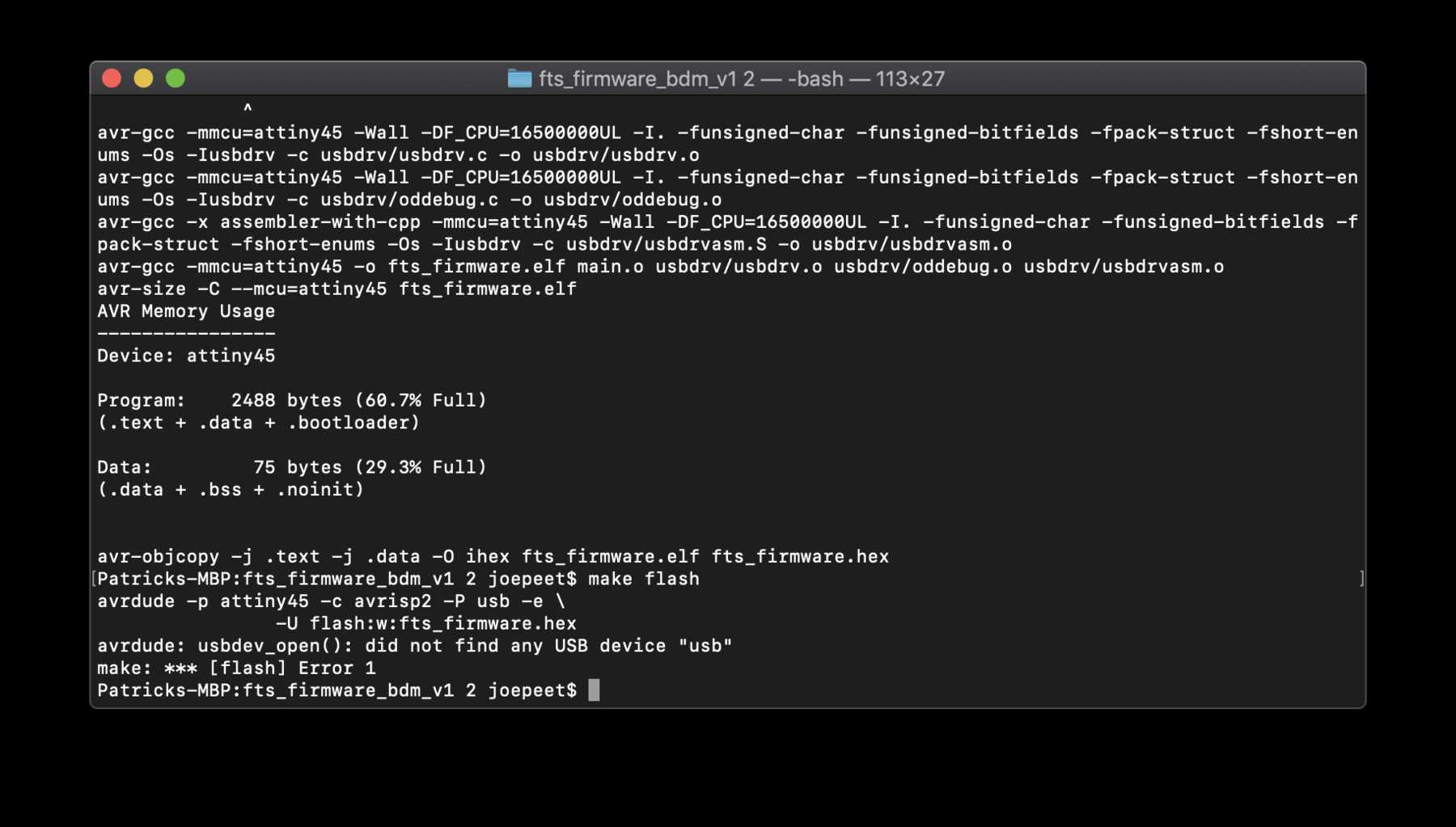
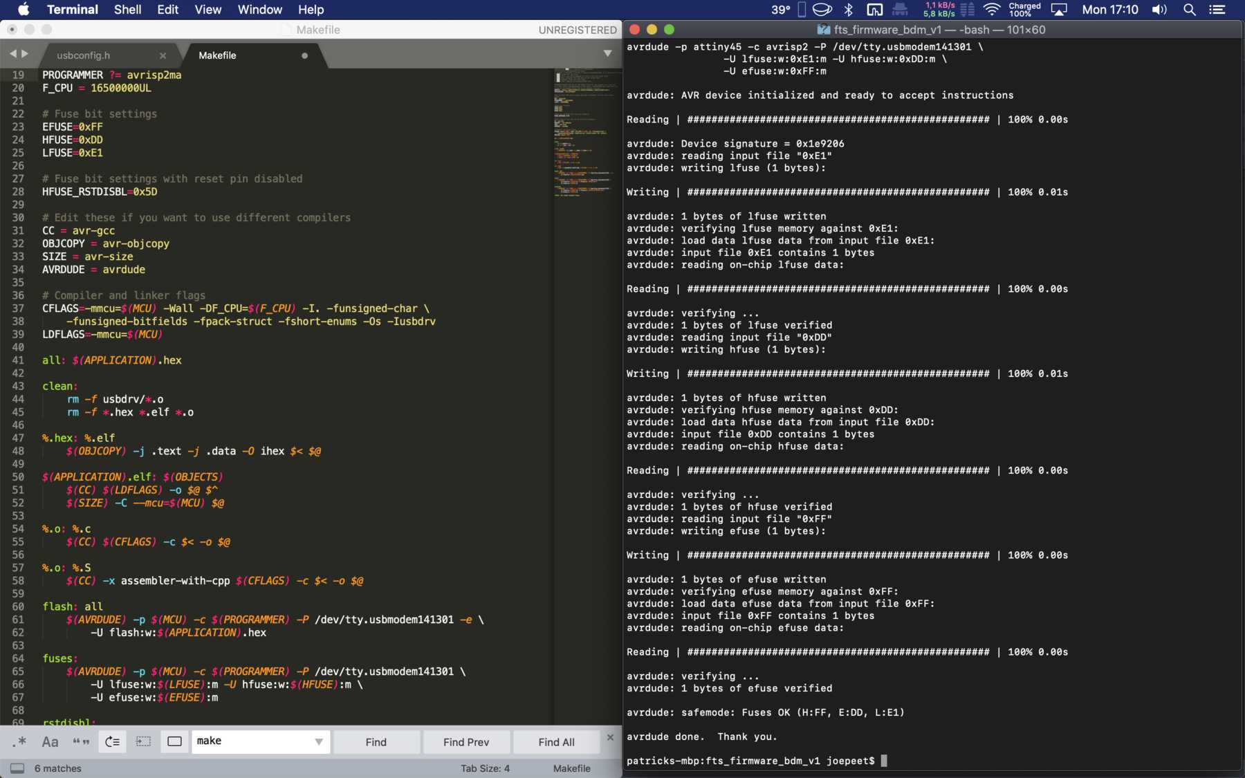
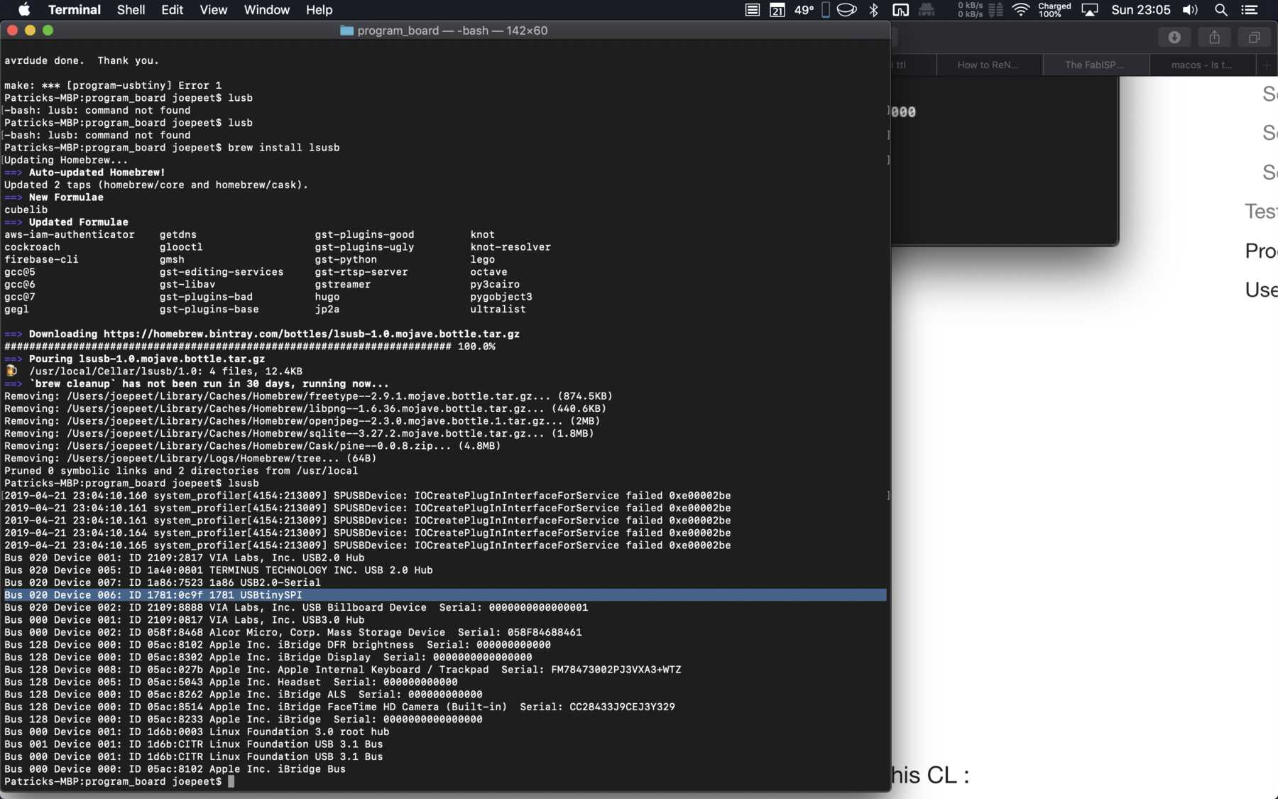
AVRDUDE had the problem with me that no device could be found independently. So I had to address the devices directly. The command ls /dev/tty.usb* showed me the connected devices. This allowed me to identify the AVRISP mkii.
I opened the file with Sublime Text and changed the lines, that AVRDUDE addressed the device directly. The code then looked like this to me:
Then I executed the command make, make flash, make fuses and finally make rstdisbl. Everything worked then and I didn’t get an error message.
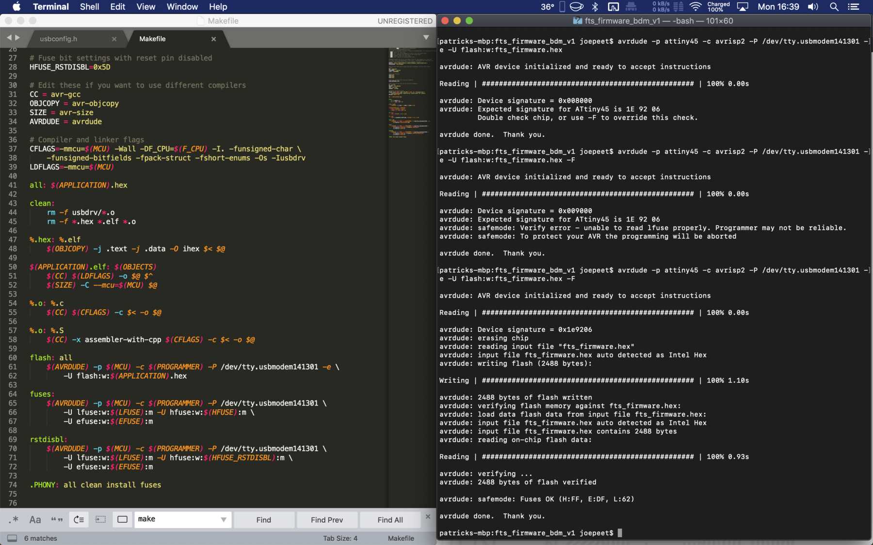
Last but not least, I tried to see if it worked. And yes, it worked! It was displayed reasonably and was also used in the following assignments. So I was more than happy that it worked on the first board.
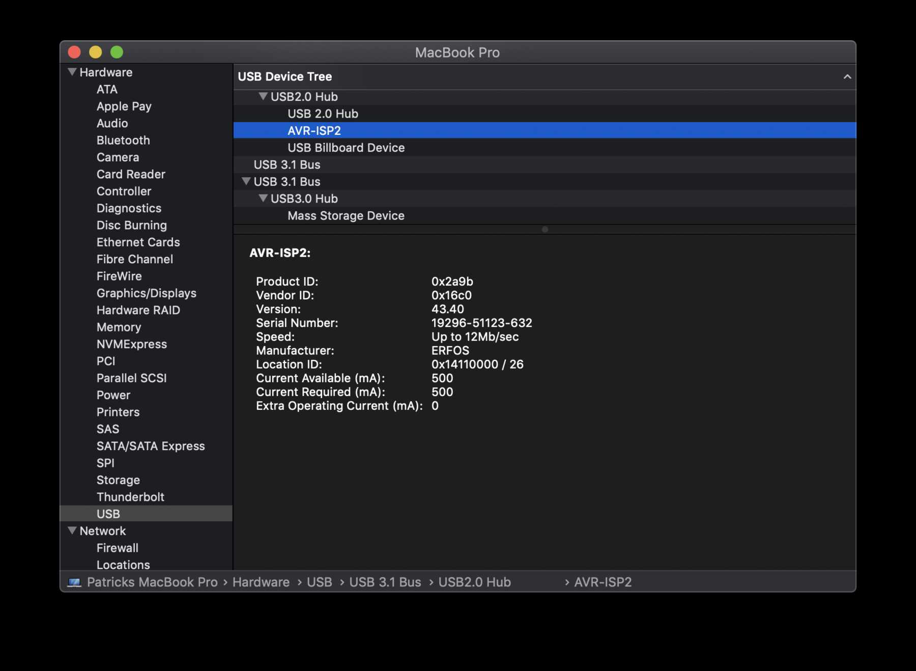
A note: The FabTinyISP is not displayed in the /dev/ list. I always used lsusb for this, which can be found here. So you could be on the safe side that it is also displayed, an alternative to “system information” on the Mac.
Here you can download the EAGLE files for the FabTinyISP:
EAGLE files