#6 Electronics design
I had lots of fun with the electronics production assignment, so I knew this would be a great one. It was more challenging, especially when coupled with the design part, but still very straightforward. I still had some little problems, though, but at the end I solved them and got my PCB nicely done.
I downloaded the Eagle 7.2.0 and after some guidance from my instructor I went through the assignment. The program is very friendly. Once you get the basics of electronics, it is just like using a graphic design program.
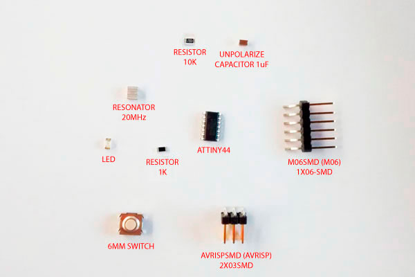
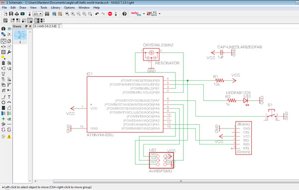
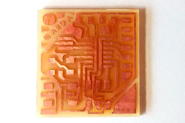
First you have to go through the schematic stage. All the component form the FAB library are added and then connected. In this stage the position of the components its not that important, but a nice distribution will help get a better visualization. It is important to make sure that all the components are connected by moving them and checking if the wires move along. There is also an option where the errors can be checked.
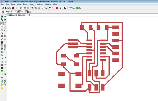
Afterward you go to the board stage. Here comes the tricky part, for all the components must be clearly displayed in order to create the paths. These paths must not be too far away each from another in order to maximize space, and no too close together because inner space is needed for drawing the path. The autorouter can also be used, but wiring everything is actually the fun part. You can also get some inspiration on the work done by those who came before you.
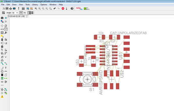
It is a good idea to check the distance between the paths with the DRC option.
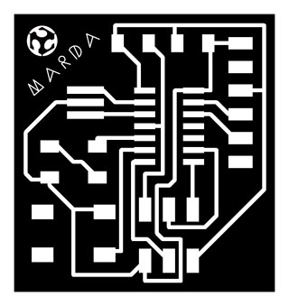
When you are done export your file as an PNG image.
I opened my file on Photoshop and created the outline.

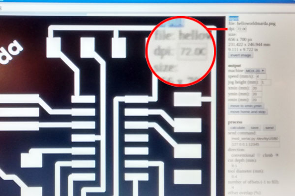
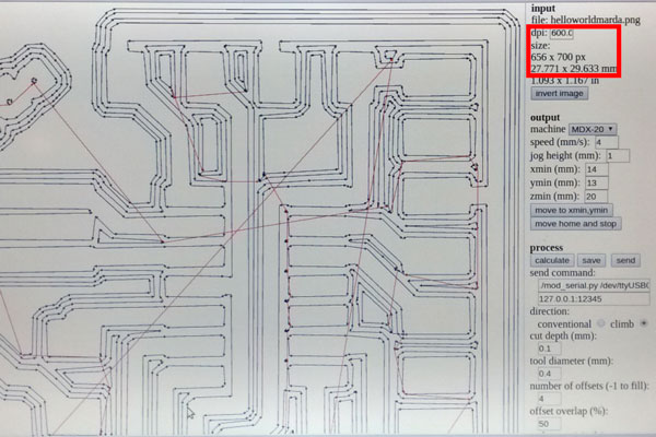
I used the latest version of FabModules.
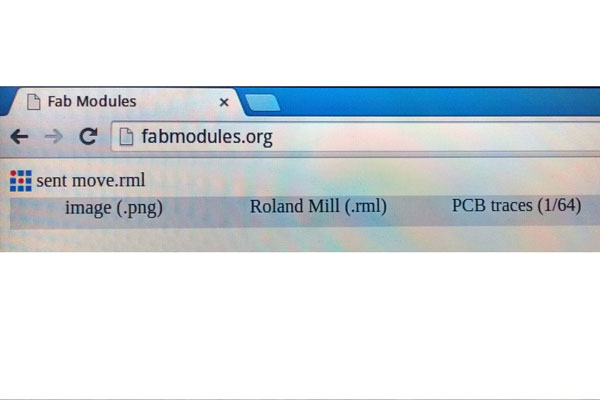
I made sure to remember the dpi parameters so it would mill at the original scale.
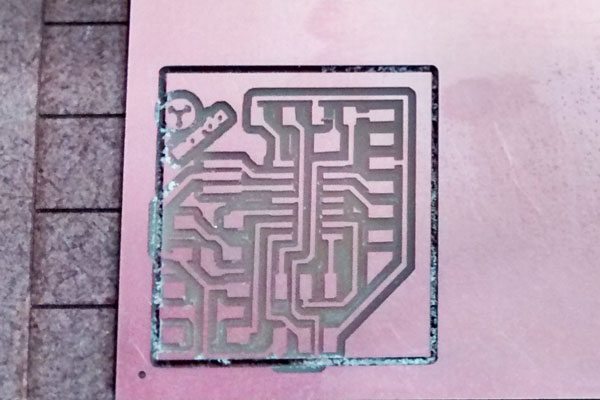
I noticed there was a mistake, though. I had generated a bigger file, so when I made the cut with the mill it cut from the origin point of the path, damaging some of the other paths. So I had to make one file including the board design and the outline, and then save both files separately, ending up with same size files, so that they would both enclose perfectly when it was time to mill them.
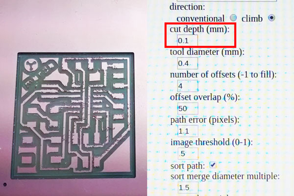
My board was milled beautifully, but I had a hard time cutting it off. I tried it a few times and nothing happened. The problem was that the cut depth was set at 0.1mm and it had to be at 0.6mm.
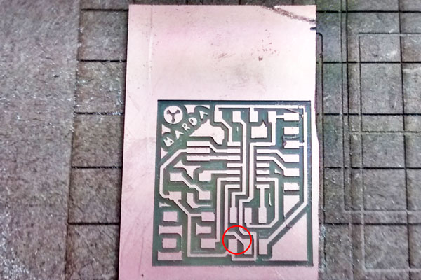
Finally, when I solved the cutting depth problem and had my PCB nicely cut, I noticed that one path was touching with another one by one corner. This could be a serious problem that could generate a short circuit. So I separated them with a cutter and everything went well.
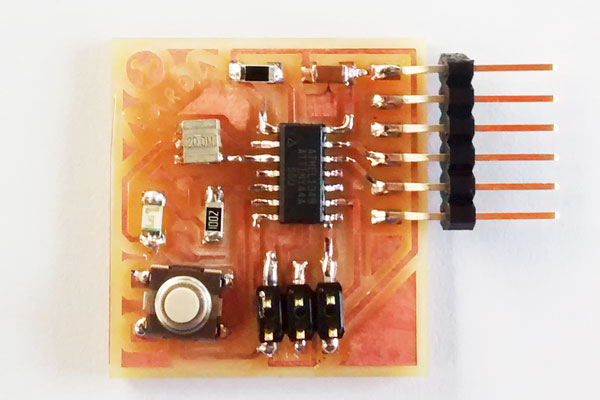
At the end came the very fun part of soldering. I had completed my assignment, and was now waiting impatiently to program it.