Electronics Design
The task for this week was to redesign the hello-world board and ada a button and LED.
After installing Eagle and the fab-libraries on Ubuntu, we started to design our boards.
My board turned out like this:
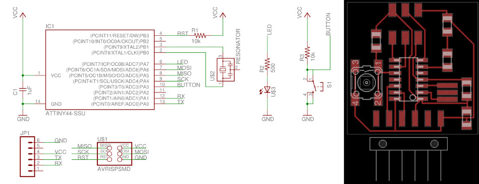
After hiding all layers apart from top and pads I exported the image with 1000 dpi monochrome as png.
I used the Gimp for adding a 2mm border around the image, that gives space for cutting out the board. The image for the cutout was produced by inverting the colours of the traces and erasing everything but the border.
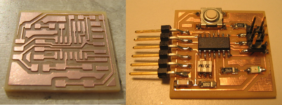
Milling and stuffing the board worked flawlessly… at least that is what I thought.
It took another two weeks, until we started programming the board, till I realized that there must be something wrong.
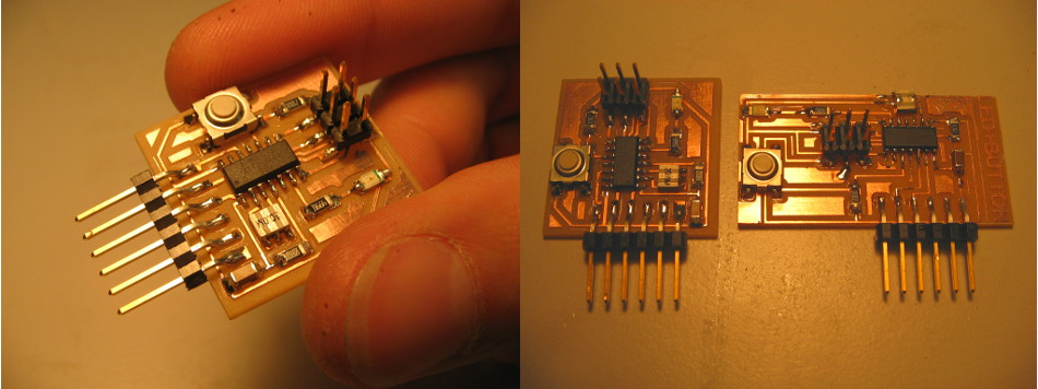
Actually you can see it quite nicely in the pictures that I soldered the ftdi-connector one step too far on the right. There was a leftover island from milling that looked just like a pad and I almost completely destroyed all the work.
Luckily I was able to desolder it nicely and solder it one further to the left.
In the future I will be very carefull where to solder my components!
On the left you can see the board between my fingers and on the right a comparison to the board that Luis designed.