7. Electronics design | MyMiniBoard_X14
Use the test equipment in your lab to observe the operation of a microcontroller circuit board (in minimum, check operating voltage on the board with multimeter or voltmeter and use oscilloscope to check noise of operating voltage and interpret a data signal). Document your work (in a group or individually):
Group assignment page: here.
My individual part: I have documented it in the Probing a microcontroller section.
Redraw one of the echo hello-world boards or something equivalent, add (at least) a button and LED (with current-limiting resistor) or equivalent input and output, check the design rules, make it, test it:
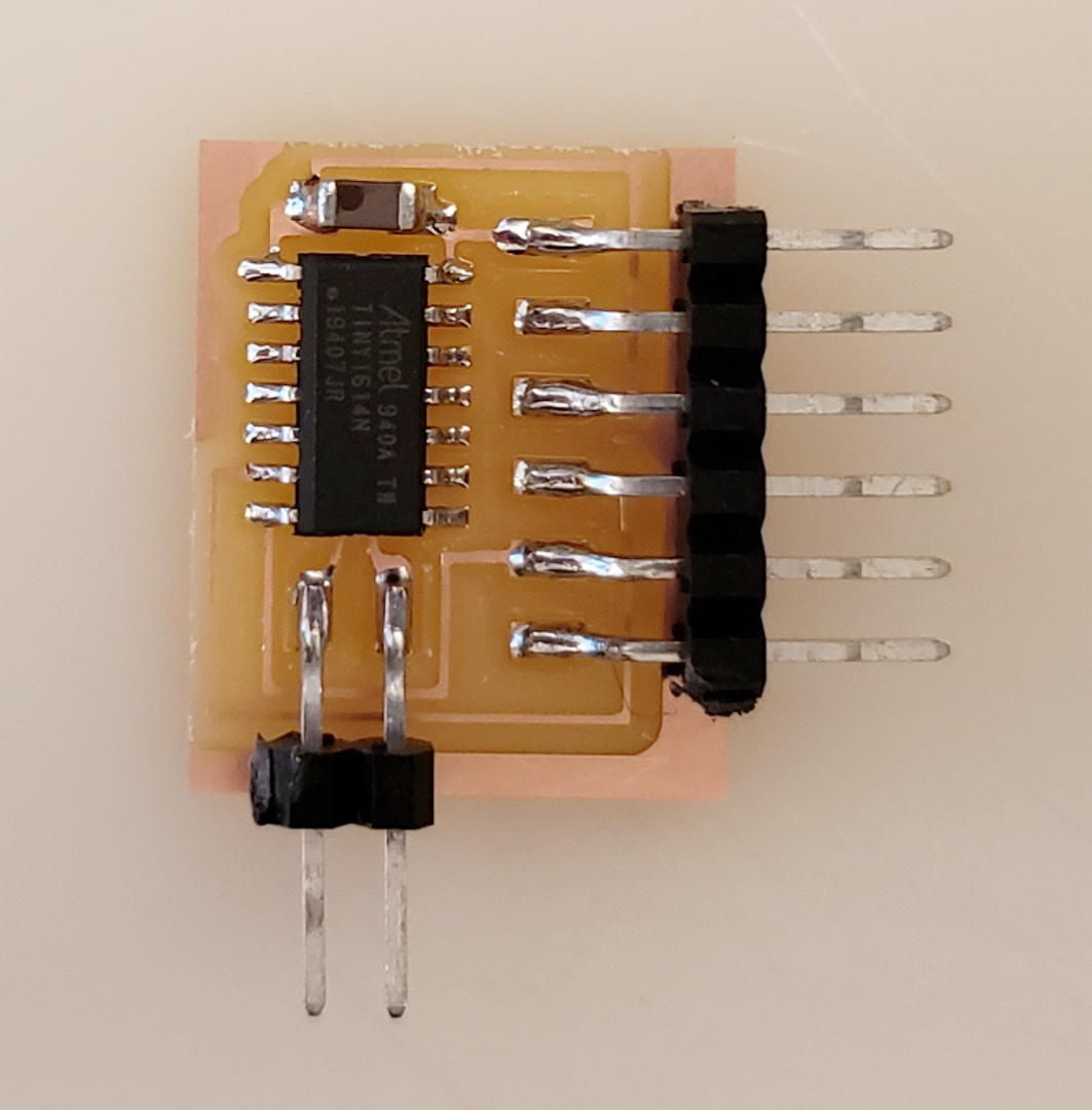
Based on the ATtiny1614 and inspired by the HelloD1614 board.
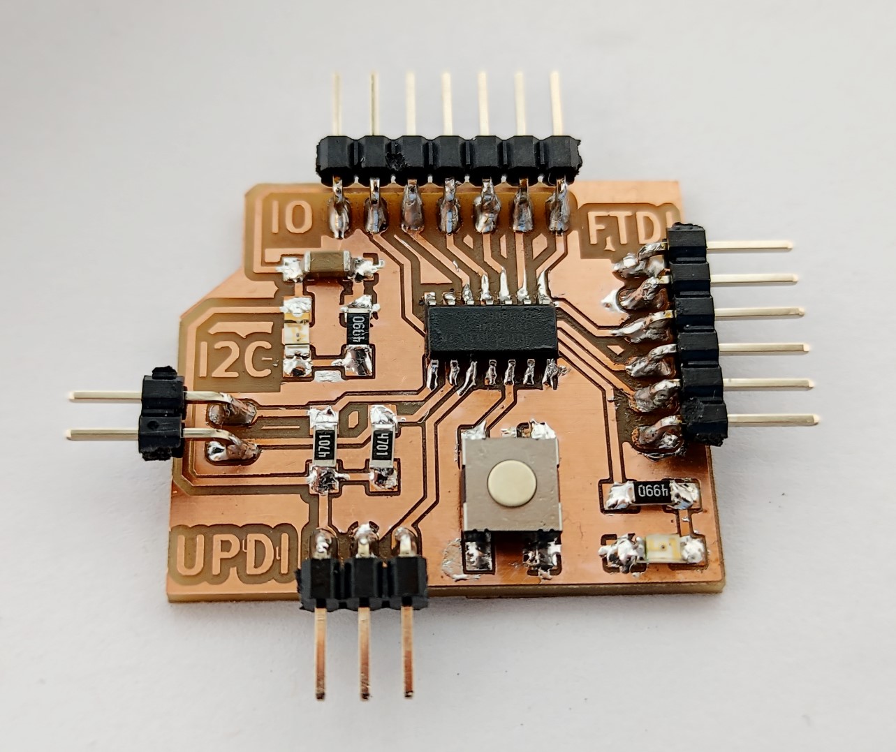
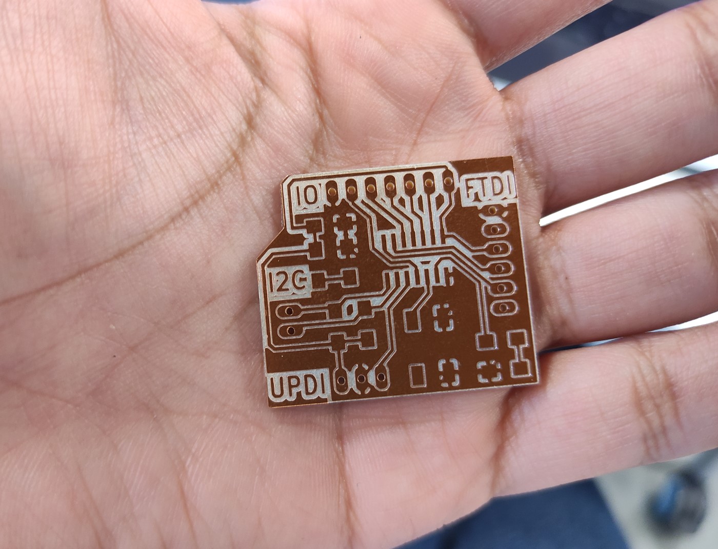
MyMiniBoard_X14 is a simple and compact board that can be used to test the features of the ATtinyX14 microcontrollers with didactic practices using sensors and actuators.
Board features
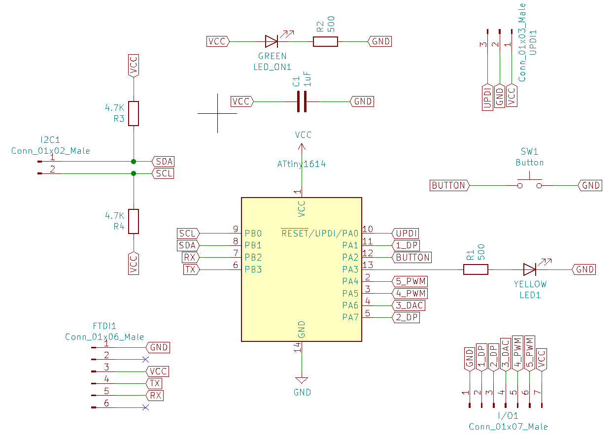
MyMiniBoard_X14 uses all of the pins of the ATtinyX14 microcontroller:
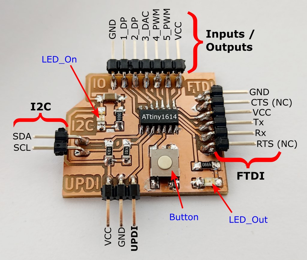
Take in account that tags for FTDI connection refer to the incoming device.
- NC = No connection
- DP = Digital pin
- DAC = Digital-to-analog converter
Description:
- Microcontroller: ATtiny1614
- FTDI connection.
- I2C connection.
- UPDI connection + VCC + GND.
- 5 Input/Output pins + VCC + GND.
- Onboard Input: Button, using the internal pull-up resistors.
- Onboard Output: LED_Out.
- LED_On: is just a LED to indicate when it is connected.
1uF capacitor to filter the noise in VCC.
4.7kOhms resistors for I2C connection.
Resistor for LEDs, as is well known, should be calculated, but since it’s a learning practice, for prevention we are advised to used 499Ohms resistors.
Coding pins
The following table describes the relationship between the board pinout (including onboard LED and Button) described above and the microcontroller pin number, that will be used when coding:
| Board Pinout | Arduino p. pin | C programming pin |
|---|---|---|
| 1_DP | 8 | PA1 |
| 2_DP | 3 | PA7 |
| 3_DAC | 2 | PA6 |
| 4_PWM | 1 | PA5 |
| 5_PWM | 0 | PA4 |
| Tx | 4 | PB3 |
| Rx | 5 | PB2 |
| UPDI | 11 | PA0 |
| SDA | 6 | PB1 |
| SCL | 7 | PB0 |
| LED_Out | 10 | PA3 |
| Button | 9 | PA2 |
Based on the ATtinyX14 pinout information.
ATtinyX14 pinout
For this practice I used the ATtiny1614 from the ATtinyX14 series, but since they have the same pinout, any of them can be used on this board.
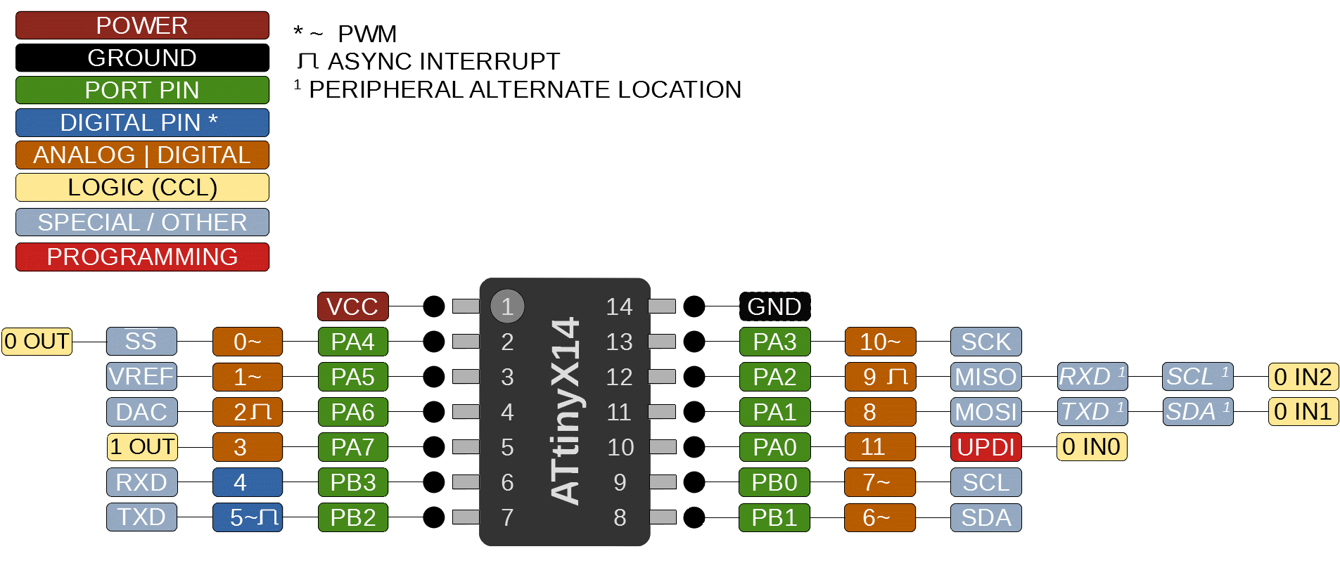
| Specifications | ATtiny214 | ATtiny414 | ATtiny814 | ATtiny1614 |
|---|---|---|---|---|
| Flash (program memory) | 2048 bytes | 4096 bytes | 8192 bytes | 16384 bytes |
| Flash w/Optiboot | 1536 bytes | 3584 bytes | 7680 bytes | 15872 bytes |
| RAM | 128 bytes | 256 bytes | 512 bytes | 2048 bytes |
| EEPROM | 64 bytes | 128 bytes | 128 bytes | 256 bytes |
| Bootloader | Optiboot (optional, not recommended) | Optiboot (optional, not recommended) | Optiboot (optional) | Optiboot (optional) |
| GPIO Pins | 12 (11 usable) | 12 (11 usable) | 12 (11 usable) | 12 (11 usable) |
| ADC Channels | 10 (9 usable) | 10 (9 usable) | 10 (9 usable) | 10 (9 usable) |
| DAC | Yes | Yes | Yes | Yes |
| PWM Channels | 6 | 6 | 6 | 6 |
| Timer Type B | 1 | 1 | 1 | 2 |
| Timer Type D | Yes | Yes | Yes | Yes |
| Interfaces | UART, SPI, I2C | UART, SPI, I2C | UART, SPI, I2C | UART, SPI, I2C |
| Clock options | Internal 20/16/10/8/5/4/1 MHz | Internal 20/16/10/8/5/4/1 MHz | Internal 20/16/10/8/5/4/1 MHz | Internal 20/16/10/8/5/4/1 MHz |
Material taken from SpenceKonde.
Board design
The software I used for it was KiCad.
Requirements, considerations and component selection:
-
I used the ATtiny1614 microcontroller cause it has the a fair amount of pins for testing different features, input and output devices for developing more specific boards for specific applications.
-
I2C communication.
-
UPDI connection for programming.
-
FTDI connection for serial communication.
-
1uF capacitor for voltage stabilization.
-
A LED to indicate when it’s connected.
-
Vcc, GND and Input/Output pins.
-
Built-in button and LED for basic programming tests.
Schematic
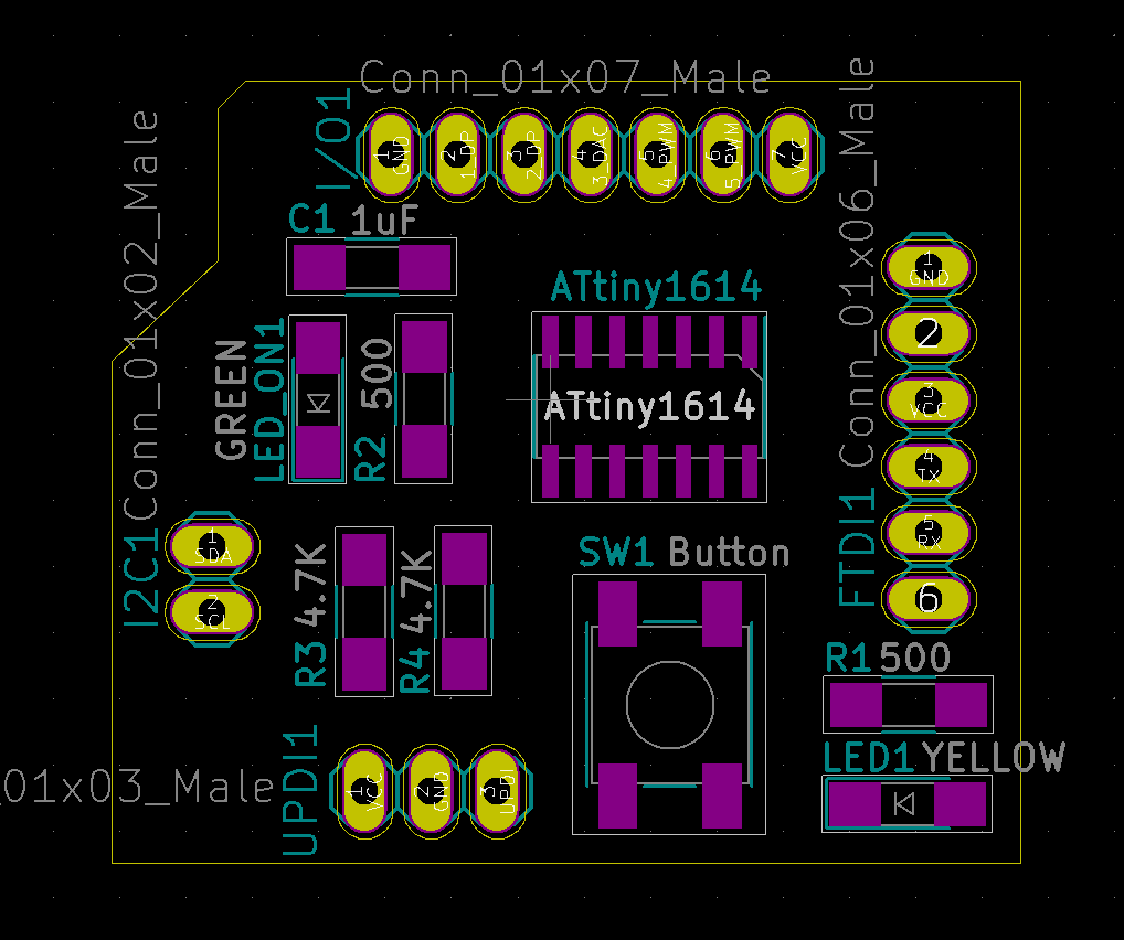
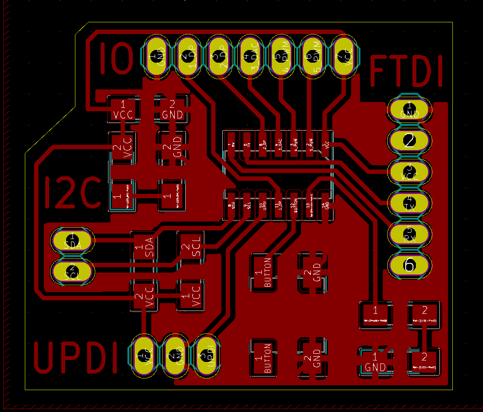
Board layout
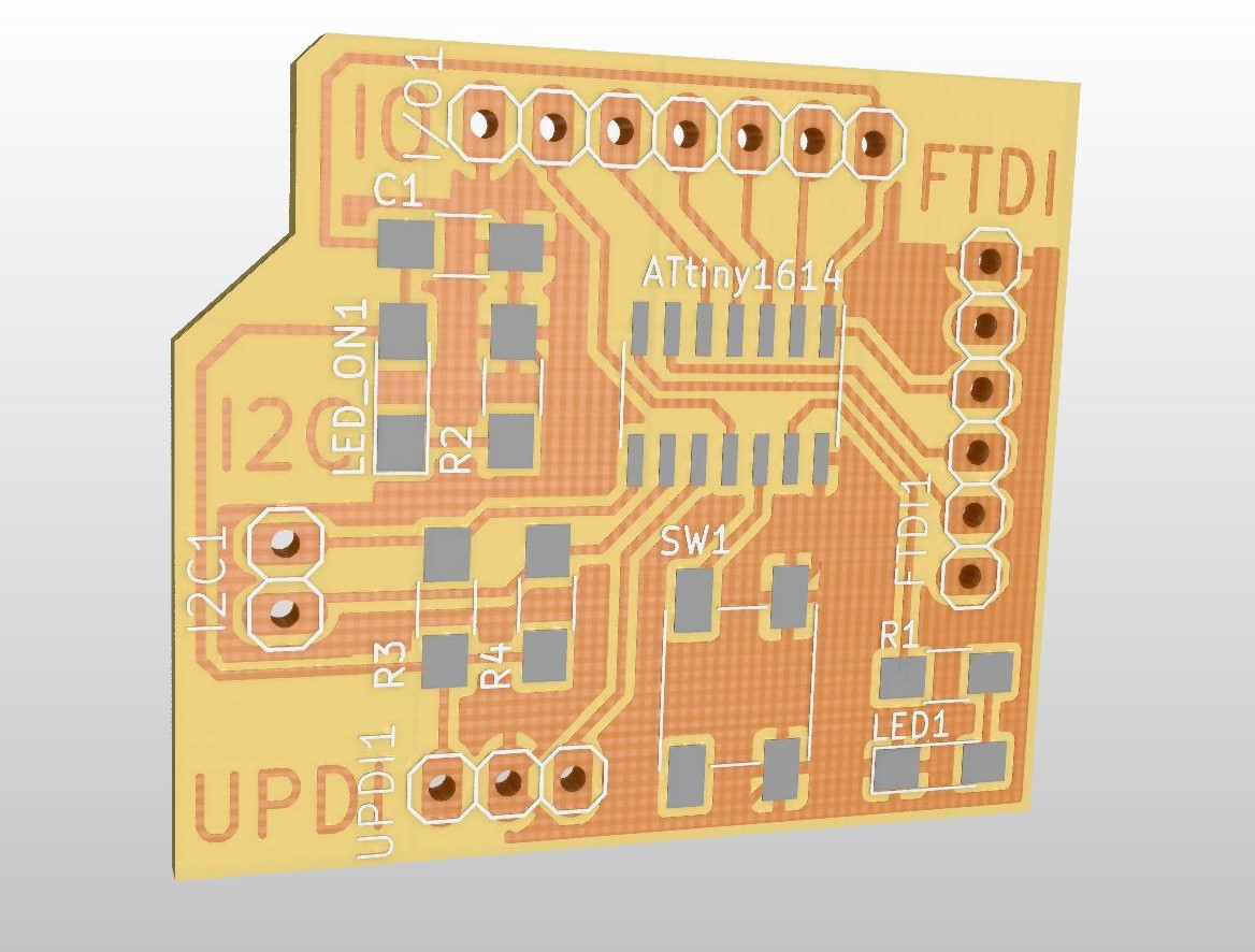
3D view of the board
I just found interesting the fact that we can also have a 3D version of the board.
Milling PCB
I manufactured the board by milling.
Images:
- Traces:

-
Holes:

-
Outline:

Result:
I used:
- Milling machine: MonoFab SRM-20
- Tool: V-bit 0.2-0.5mm
Components
SMD = 1206
| Quantity | Component |
|---|---|
| 1 | Microcontroller ATtiny1614 |
| 1 | Capacitor 1uF |
| 2 | Resistor 4.7KOhms |
| 2 | Resistor 499Ohms |
| 1 | LED Yellow (LED_Out) |
| 1 | LED Green (LED_On) |
| 1 | Button |
| 18 | Single row right-angle male pin header |
Programming
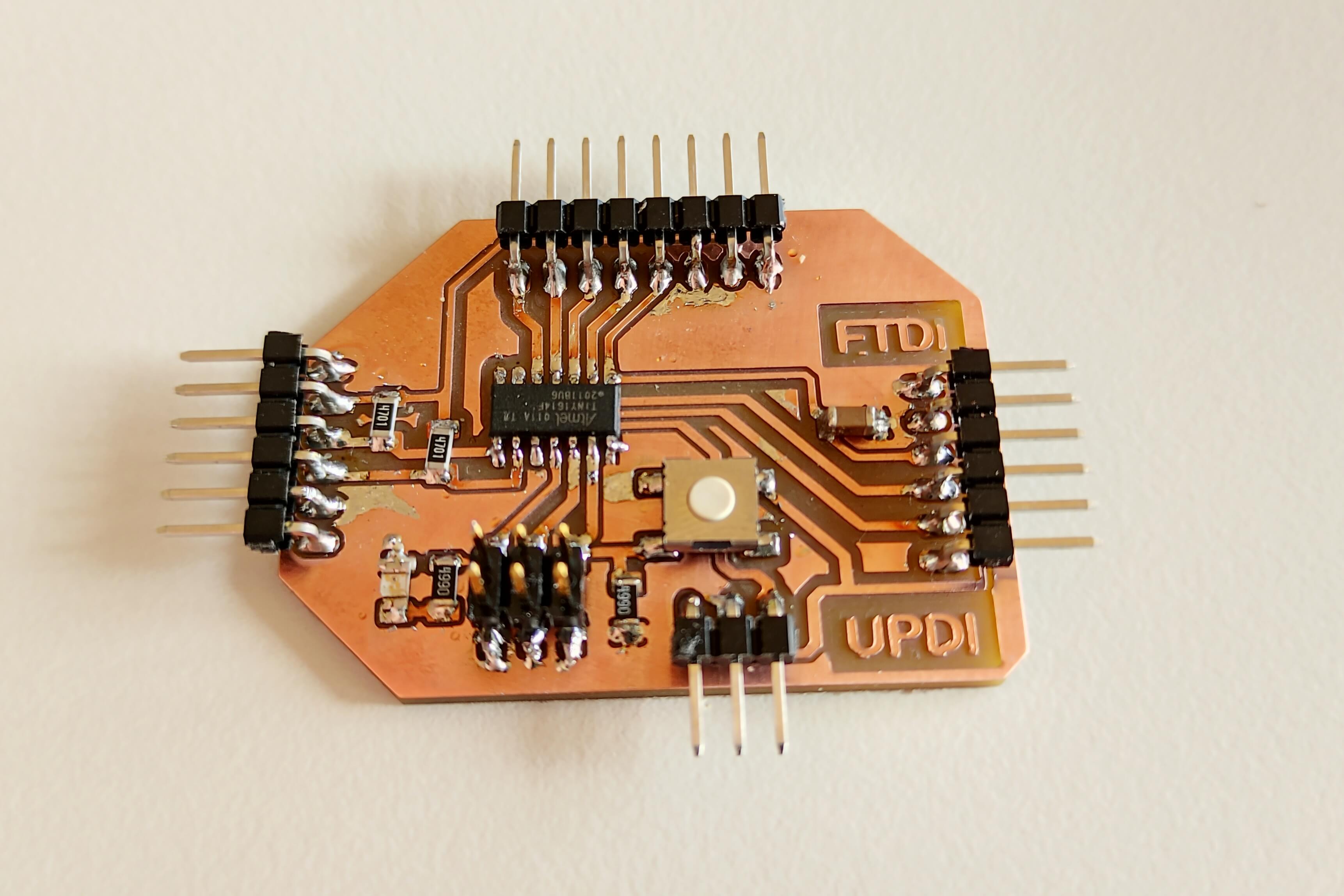
Connection
I connected it via UPDI using the FTDI-USB and UPDI-3 boards that I manufactured during the Electronics production week:
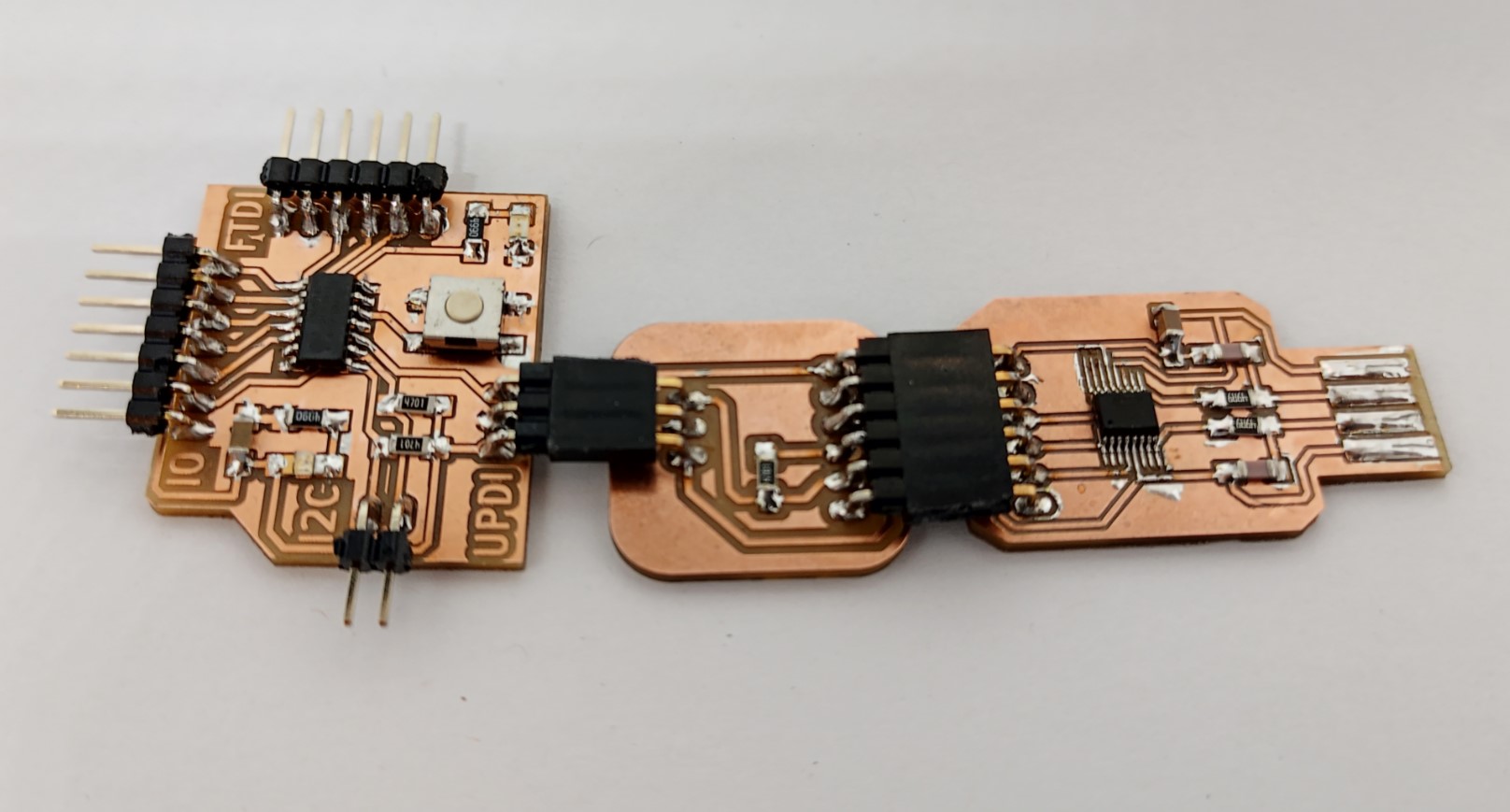
It’s recommended to use an USB extension or hub for connecting to the PC.
First settings
For the first time we need to add the MegaTinyCore to the Arduino IDE:
- Open the Arduino IDE.
- File > Preferences
- Paste the following link in Additional Boards Manager URLs: http://drazzy.com/package_drazzy.com_index.json
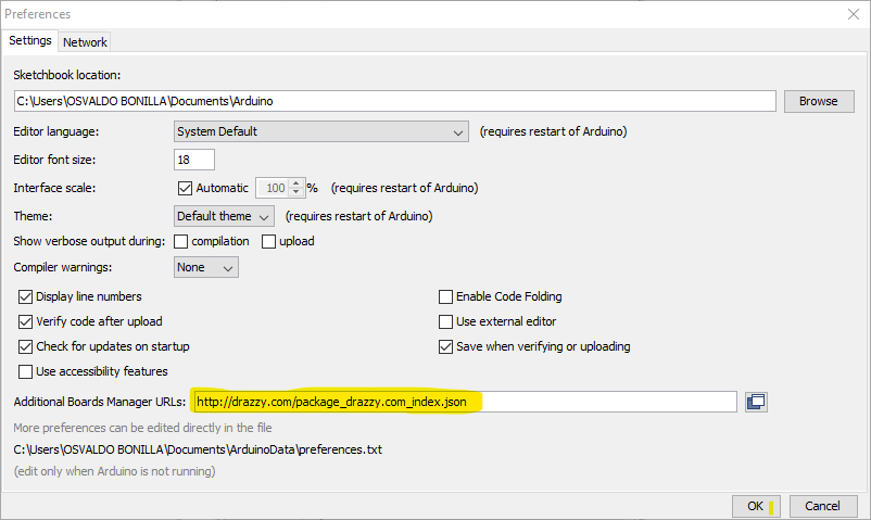
- Press OK
- Tools > Board > Boards Manager
- Search for MegaTinyCore (by Spence Konde):
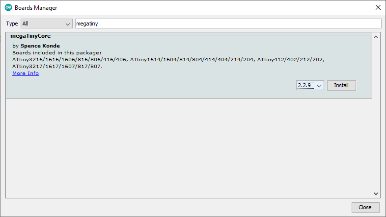
The latest version when I made it was the 2.2.9, which I had some issues with (very long installation time and then no compiling); version 2.2.8 presented no problems at all. Take in account that the only test I made was the Blinking with the onboard LED.
Test code
I tested it with a basic Blinking LED:
1 2 3 4 5 6 7 8 9 10 11 12 13 14 15 16 17 18 19 20 21 22 | |
Upload a Code
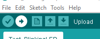
-
To upload a code to the Board, we just need to use the following highlighted settings in the Arduino IDE:
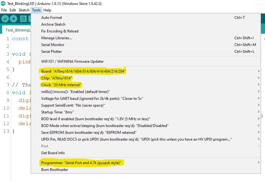
-
After selecting these options and when testing the board by the first time, press Burn Bootloader to setup the Microcontroller; then you can just press the Upload button:
Performance
Probing a microcontroller
I have used the Hello boards that I have manufactured during the Electronics production:
Checking operating voltage with a multimeter:
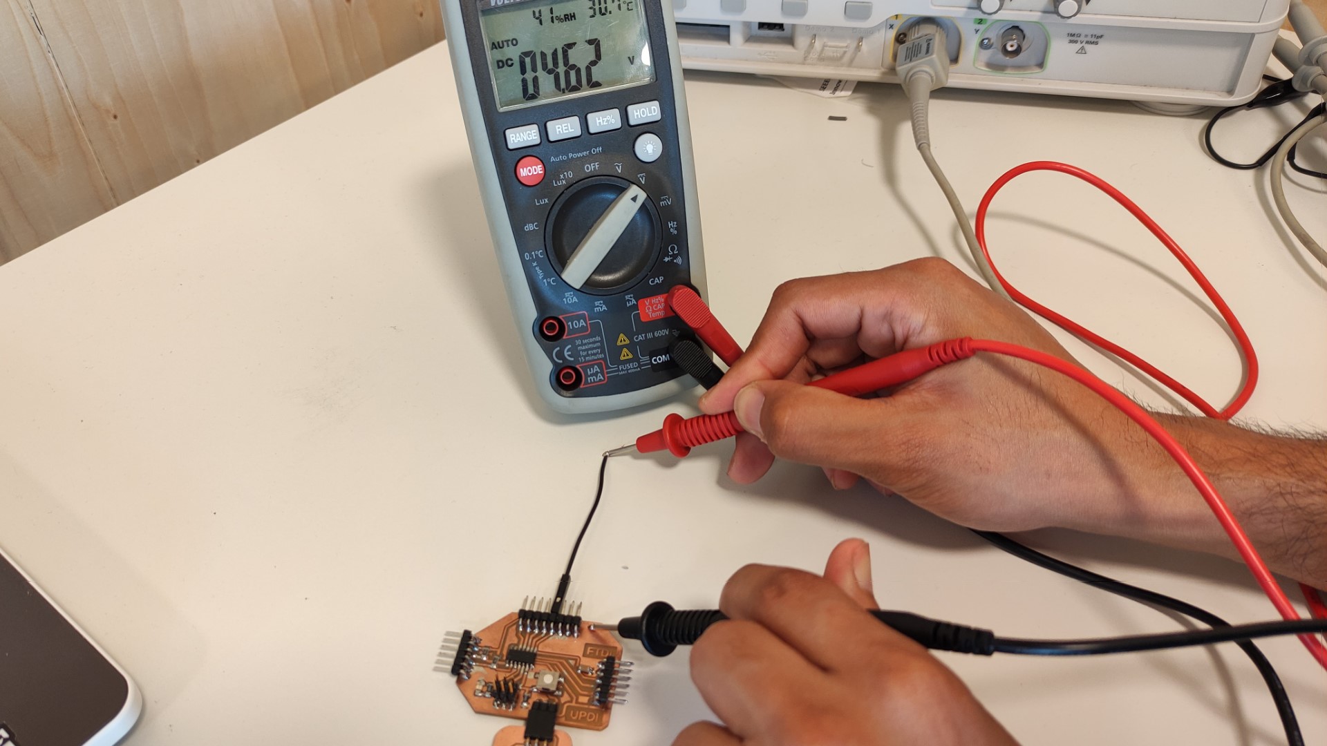
Result: 4.62V
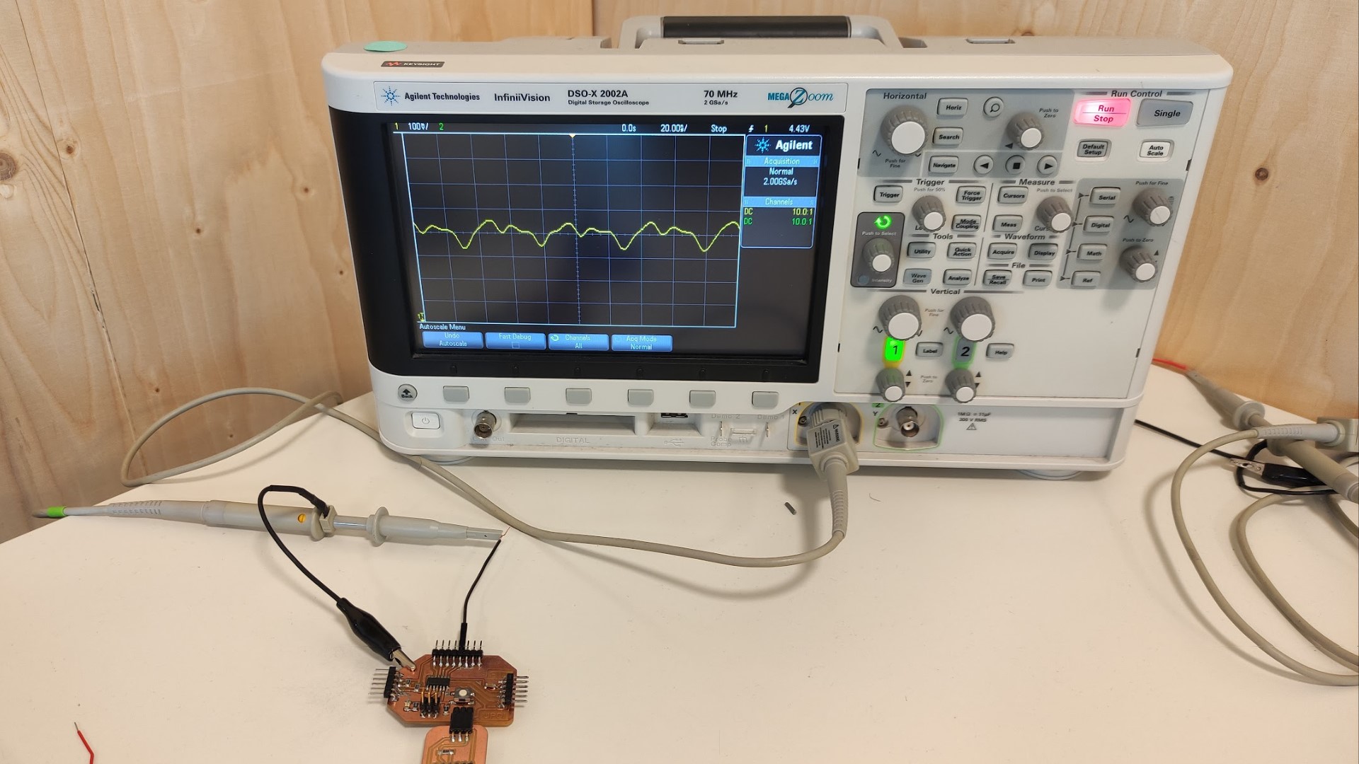
Checking noise of operating voltage with an oscilloscope:
For this task I wanted to see the difference that a capacitor makes in the noise of the operating voltage, then I have made a first test with with the 1uF capacitor, I removed the capacitor and made the second test:
-
Test 1
Test with capacitor:
-
Test 2
Test without capacitor:
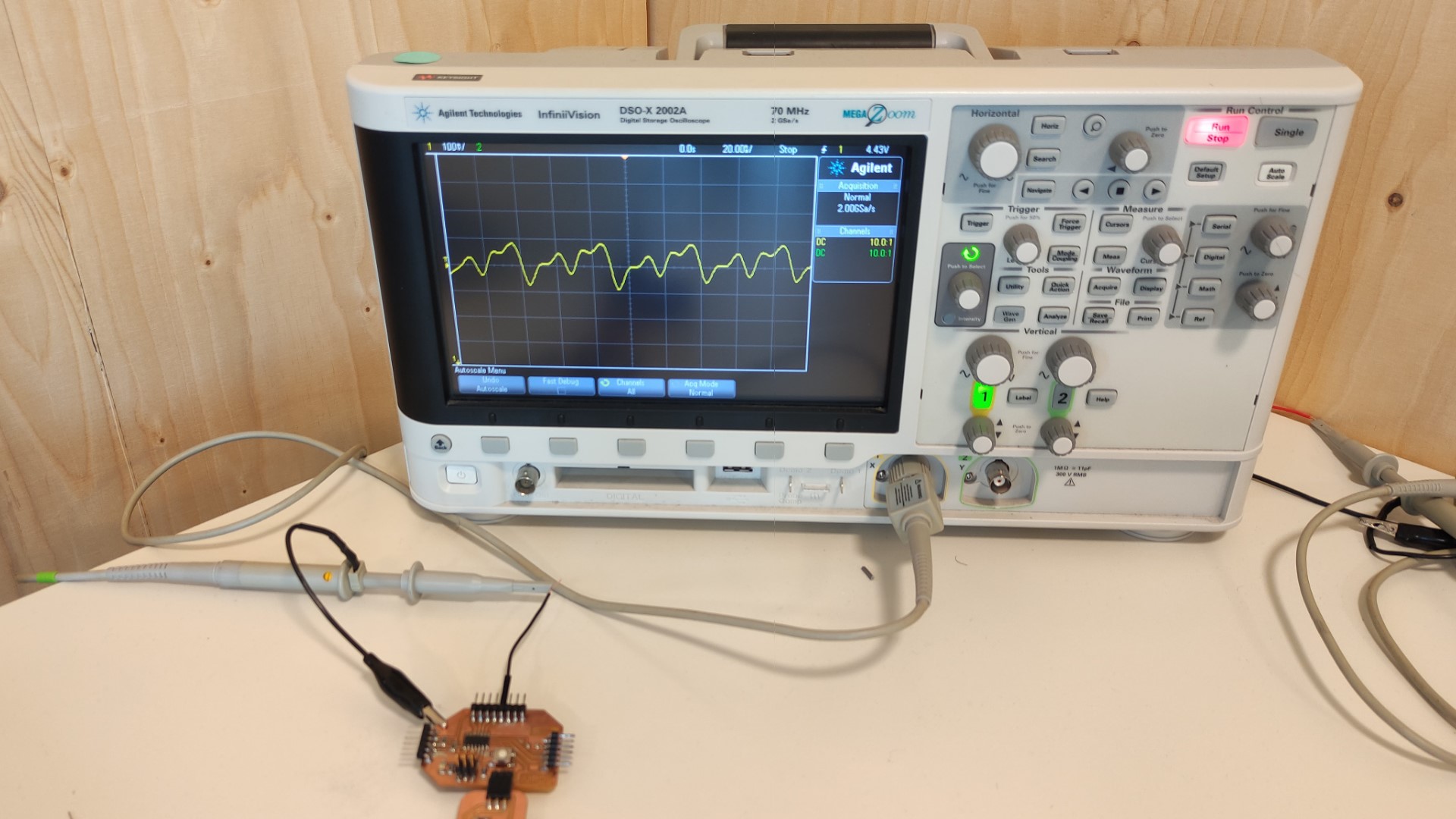
Even with the capacitor there is noise, but the peaks are less pronounced in comparison.
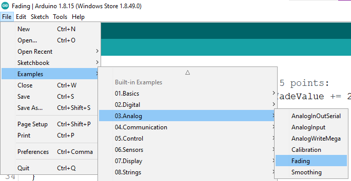
Interpreting a data signal:
For this task I have used a “Fading code”, based on a Fading example code:
Code block:
1 2 3 4 5 6 7 8 9 10 11 12 13 14 15 16 17 18 19 20 21 22 23 24 25 26 | |
- The code fades out from max to min, then fades out from max to min a LED.
- The LED on this board is on a digital pin, so I cannot show that effect on the LED.
- I have edited the code adding a second pin as output, then now I apply the fading effect to one digital and one PWM pin to see what happens.
Practice
- I connected Channel A to the PWM pin, and the Channel B to the digital pin:
I have set a different magnitude in the Vertical axis for the channels so I can clearly see both of the signals.
- This is what happens if we try to apply PWM to a pin that is not made for it. It will only offer High and Low output signals.
- If a LED was connected to pin 0 (the yellow signal in the oscilloscope), it would lower and raise its light intensity.
- If a LED was connected to pin 3 (the green signal in the oscilloscope), it would just turn on and off.
Assignment outlook and details
I have worked a bit with Eagle before, but this was my first experience with KiCad, I learned the basics of how to work with it during a lecture with my instructors.
I haven’t add details of “how I did it” throughout the documentation cause I like how it looks like this, just a page that explains the features of it, and offers the necessary to replicate it (and of course, proof that it works 😅).
A mental note I got from this experience for future boards was… use wider clearances or you will have issues when soldering and will probably have short circuits. Despite it didn’t result as clean as I would have liked… I’m proud of my board 😄.
Schematics:
The most common commands when making the schematic are:
-
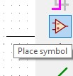
Place symbol to select a component:
-
Place wire to connect the components:

-
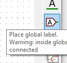
Place global label indicate connection between components when using only Wire could result in a confusing result:
-
After the layout it’s necessary to specify the footprint for each component:
Board layout:
There are some recommendations to consider in order to get a good layout, effective routing and error-free soldering.
Component orientation: Orient similar components in the same direction.
Organization: Place all of the surface mounted components on the same side of the board. All trough-hole components should be on the top side of the board.
Power and Ground Planes: It’s recommended to have power and ground lines internal to the board, this will help to prevent the board from bending.
Routing: It’s recommended to always place the traces as shortly and directly as possible between the components (important to consider during the organization step).
Net Widths: Minimum 0.254mm for low current signal. Traces that carry more than 0.3A should be wider, we can use a trace width calculator to determine it according to our application.
Clearance: By experience I can tell that when making PCBs by milling… make sure that the clearance is at least the same width of the milling tool, if it’s smaller it wont be taken in count by the g-code generator.
Commands:
When making the layout, we start arranging the components.
The two commands I use the most when making the Layout are:
-
Route track to determine the physical connections of the components:

-
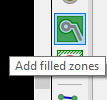
Add filled zones to fill the parts in blank as GND:
Files and datasheets
- Kicad project: MyMiniBoard_1614.zip
- Test_BlinkingLED.ino
- FadingTest.ino
- ATtiny1614DataSheet.pdf
- David Marrakchi. Top 5 PCB Design Guidelines Every PCB Designer Needs to Know