6. Electronics design
Task
This weeks task was to mill a variation of the HelloWorld boards utilizing an ATiny chip except with the addition of an input and output, which in my case was a button. I would design a schematic in Eagle CAD using the Fab.new.lbr. This library allowed me to begin the schematic and and create the board then I would mill solder and program the board to complete the rest of my assingment.
Prior to completing the assigment at hand my class practiced using Oscilloscopes. For the group assingment, I first learned how they worked and what their purpose was. I then ran through the process on my own of measuring the voltage of a servo motor with a variable resistor. I first connected the probe of the Oscilloscope to itself to get a base line voltage value. I then set the range of values on the Oscilloscope to best view the data. Once this was all done I connected the probe clip to the ground of the circut I was measuring and the probe to the data. As I changed the value of the resistor I watched as the voltage length grew in length and shortened. Group site found here.
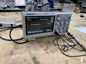
Above is an image of the baseline voltage measurement with the readings constant as I had set the result values so it would be easy to read.
Board Design
Schematic
To begin the task at hand I first picked a board that I would use as my reference for this week. The board I created was required to be an iteration of a Hello world board such as the blink board from week 4. I decided upon using an ATiny412 chip in my board and would have a button as the input and an LED as the output. To start the design process for the board I first had to begin a schematic. In order to gain access to the correct parts I first had to download and open the fab.new.lbr library into eagle. This library allowed me to use components such as the ATiny412 chip and more.
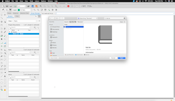
Above is the library downloaded that contained the components needed for the schematic of the board I created. Without this library I would be unnable to complete the board and mill it for this week.
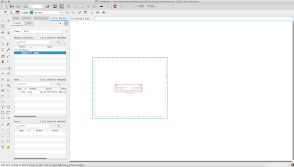
Following the installation of the library, I then inserted all the components needed into my schematic. I had to make sure I selected the correct chip and button but other than that, The resistors and capacitors I would use were all the same size, I just had to select the correct component from the library. Once I had all my components in the schematic including, 1 button, 1 chip, 1 capacitor, 1 set of headers, 1 LED, and 2 Resistors, I organized them in a fashion that would make my routing of traces neat and easily accessible.
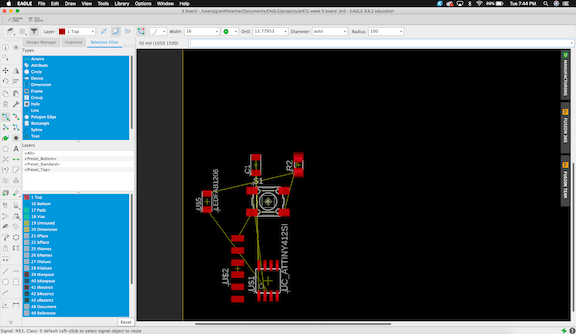
Above is an image of the first component inserted in my schematic, the ATiny412 chip. In the photo you are able to see what each pin on the chip dose itself such as the VCC ground and data pins.
Above is an image showing all the components I would connect to create the board that I am going to program. I have organized them in a fassion so the capacitor is close to the board to better smooth out the current. The rest of the components are layed out so that I can route them easily.
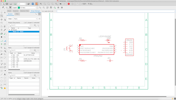
Once all of the components where in place I routed them using the route function of the schematic. For this step it didn’t matter how neat it looked as I was just establishing connections that would be created on the board itself. I had to connect the capacitor to VCC and ground the chip then back to the headers. I also had to ground the button. Once everything was connected I was ready to convert the schematic to a board.
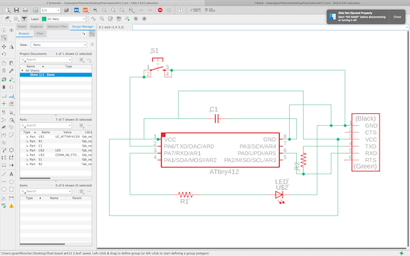
Above is an image showing the connections between each component in the board. They are all connected and ready to be converted over to a board in eagle that will then be milled.
Board
Once I had finished establishing all the proper connections within the schematic I converted it over to a board. On the board I have to orient and connect all the components. This is the file that will be milled so neatness of traces is important. For the first step I had to move the group of components that was output by the switch from schematic into the frame.
Above is an image showing what I was left with after switching to a board. The components are all jumbled up with a bunch of yellow traces.
As you can see in the photo beforehand are yellow traces. These traces are what will be milled to connect components. I had to orient the components in such a way that these traces were as straight and neat as possible so my board would connect neatly. Once I had everything aligned properly, I had to route the traces. To start I changed the trace width from 6mm to 16mm to make soldering easier. I then clicked on each component with a yellow line on it. This would highlight another component showing where I needed to connect the trace based on what I had connected in my schematic. Once I had all my traces neatly connected in a way that would function, look neat, and be easy to solder I dragged the board outline in and had a file that would be ready to mill, solder, and program.
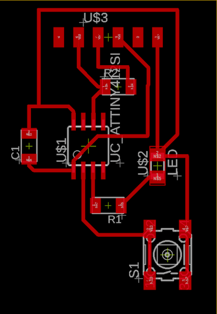
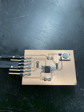
Above is the final .brd file that I exported and milled using our lab’s CNC machines. Each red line became a trace and each component became a pad too solder upon. I will then program the board to complete the task at hand.
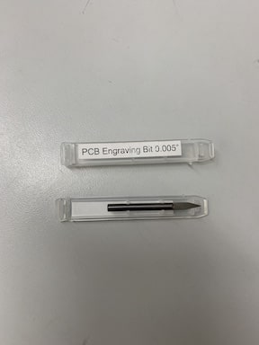
Above is ana image of just one fo the bits used in the milling process of the PCB. The bit pictured is a .005 engraving bit that I used to mill the traces of the board itself. The other bit I used was a 1/32 end mill bit that was used to make the traces wider as well as cutting the outline of the board. I used the Bantam tools software on my lab’s computers and milled my blink board. I first had to tape down the PCB material to the CNC bed. Then I locked the .005 bit into the CNC and tightened. Once this was completed I set the tool which the software had to run a program to identify. Once this was complete I used the bit breaker function to get the exact material thickness by probing and stopping once a connection was made. Once this was all completed I elected traces only and milled. Once this was finished I vacuumed the PCB and switched the bit to .32 end mill. I repeated the same process then milled just the outline. Once this was completed I had my finished board. This process went very smoothly taking around 10 minutes including set up and I encountered no problems. After milling my board I soldered it together correctly and then programmed.
Programming
In order to confirm that I completed this week’s assignment, I programmed the board using a code that would blink the LED with the press of a coded in button. First I used the programmer and the pinout for the AT412 chip to hook up the board I made. I had to change the blink code by inputting the pin that the LED connected to as well as the button input. I then compiled the code which worked successfully to show that my chip was able to receive. Finally, the code was uploaded and When I pressed the button the LED lit up and when I released the button the LED turned back off.
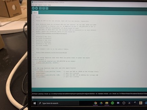
Above is a photo of the code that would use the button to blink the LED after it had finished compiling to my blink board. I now would be able to light up the LED with a press of a button.
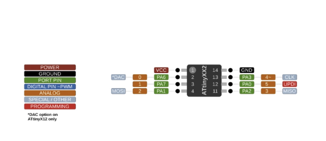
Above is the pinnout I used for hooking up and programming my blink board. My button was pin 0, my LED was pin 1 and then I connected my ground and power.
Code
Below is the code that I used to program my blink board. I wrote the input that will use the pin that my button is and detect if it is pressed to turn the light on. I also modified the code to have the output LED be set the the pin that my LED is on my board.
void setup() {
  pinMode(0, OUTPUT);
  pinMode(1, INPUT);
}
void loop() {
  if (digitalRead (1) == 1){
  digitalWrite(0, HIGH);   // turn the LED on (HIGH is the voltage level)
  delay(1000);                       // wait for a second
  digitalWrite(0, LOW);    // turn the LED off by making the voltage LOW
  delay(1000);    // wait for a second
}
else {
  digitalWrite (0, LOW);
}
}
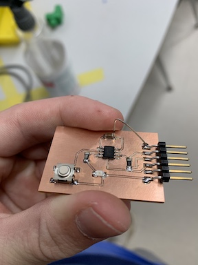
Above is the blink board completly connected and programmed. This is also a picture of my finished soldered board. I removed all bridges before connecting and testing for continuity with a multi meter.
Above is a video of my blink board functioning. This is the completed assignment for week 6 I have attached the wires programmed and proved my LED works by blinking a button.
Failures
Throughout the duration of this week I encountered my fair share of failures when it came to designing and milling my boards. One of my errors came when on my original schematic I did not have my chip connected to ground. This resulted in my button and LED being in series and short occurring between my grounds. I fixed this error by connecting the ground of my chip to the ground of my headers.
Another error I encountered my fair share of was soldering. I struggled with soldering the AT412 chip pins without forming bridges. I ended up ruining 2 boards on the chip alone due to bridges that I was unnable to remove with both wick and a solder sucker. I eventually overame this by slowing my soldering down, applying more flux, and adding solder to the iron then touching the pin with the tip of the iron.
Above is the failed board where I did not have ground connected. I attempted to resolve this issue short term by connecting the ground with a piece of wire. This solution did not work and I ultimately decided upon re-designing the schematic. The corrected schematic is documented above in my designing of the board. In the re-designed board I properly connected each trace so that my circuit was not only cleaner and would not give me problems soldering but also made it so the button press was using the chip instead of working as a flashlight. This was done by connecting my vcc and to ground as data pins. I also better organized the components and their traces in the board layout by using the manual route instead of auto route so I could avoid close traces and traces that went underneath components where it was unneeded. This cleaned up my final board very nicely and made it much quicker to solder. The re-design functioned properly using the code written to turn on the button. After milling this board I soldered it and tested and it worked first try as seen in documentation above.