Week07. Electronics design
This week, I did the following.
-
Group Assignment
- Verify the operation of the circuit created using the oscilloscope.
-
Individual Assignment
- Create circuits created by yourself.
- Write the program to the circuit with the programmer created in Week 5
Group Assignment
The content of our group assignment is here
Week07 Group Assignment
Impressions
I thought that the output of the signal of the alphabet with a clear waveform is a good example that it can be understood that the digital data consists of all 1/0.
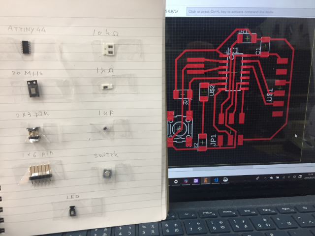
Electronics design
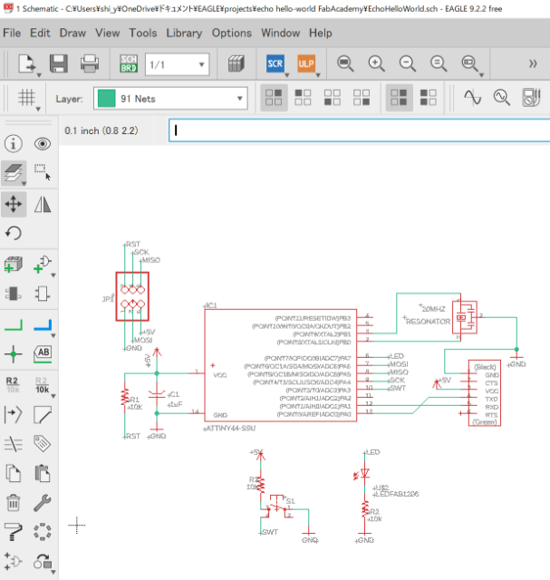
I designed the circuit using Eagle.
The procedure was as follows.
See the tutorial for usage
Project Settings
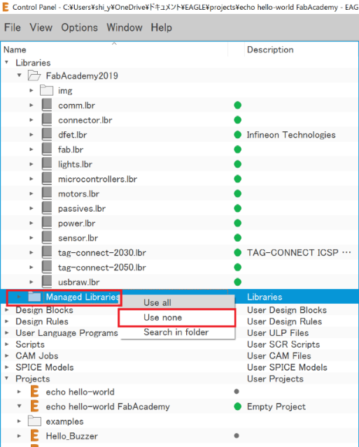
-
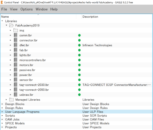
Download the library to use with FabAcademy.
-
Import library
- Options -> Directories -> Libraries
- Enter the library path
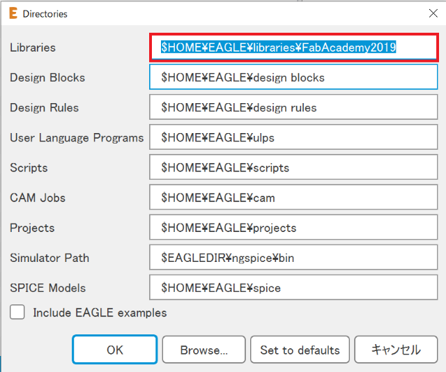
- Options -> Directories -> Libraries
-
The library is displayed.
Electronics Design
Schematic Design
-
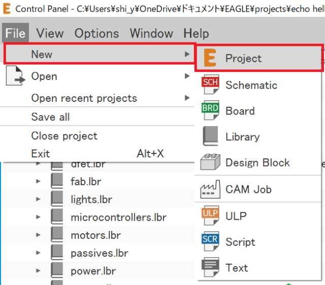
Create New Project
- File -> New -> Project
-
Create Schematic
- File -> New -> Schematic
-
Add Modules (add command)
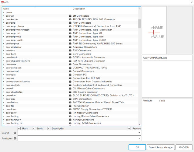
- Too Many Modules…
-
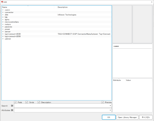
Reduce Libraries
- Select a library you do not use and select Use None
- Reduced libraries
-
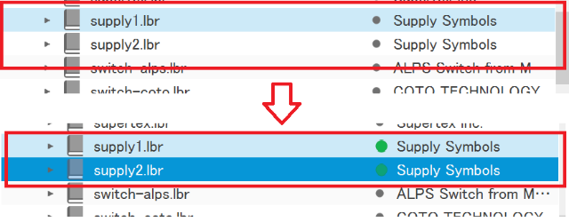
Write schematic…
- 5V&GND not found
-
Reuse Libraries
-
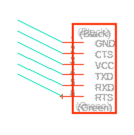
Using Modules Lineup
-
Wiring while watching the following images
-
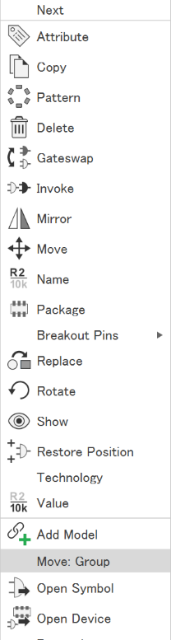
Just move it, the line does not come
-
When you move with MoveGroup, the line also comes in
-
Result
-
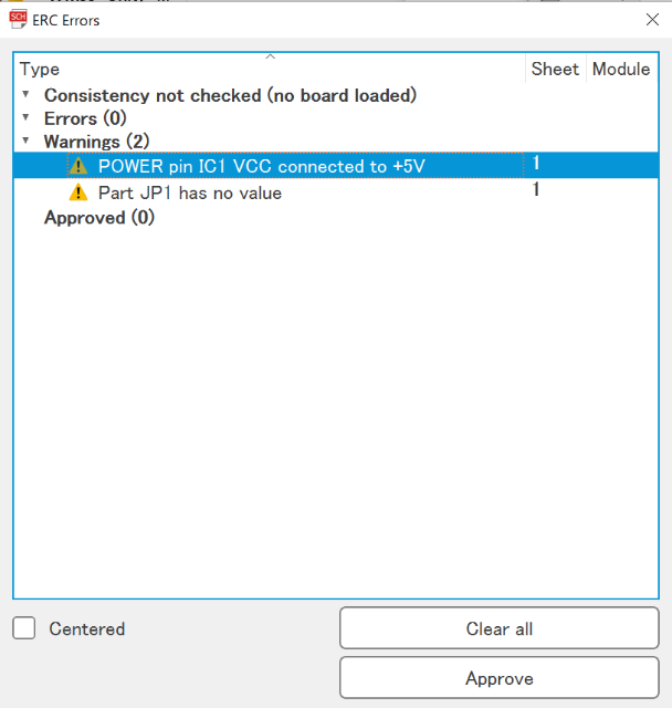
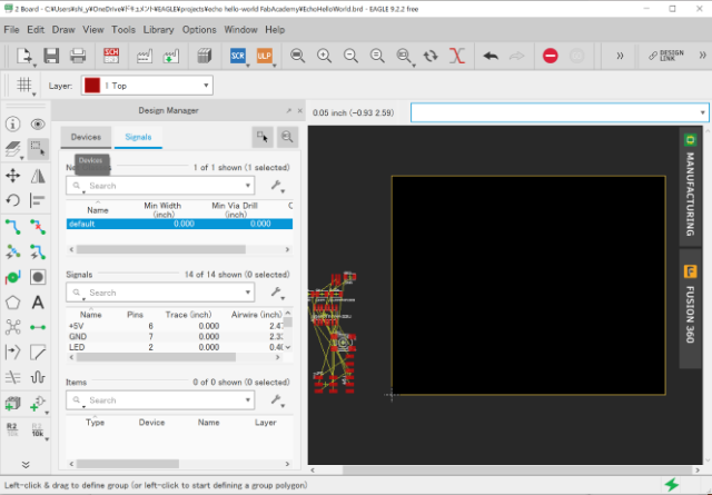
Check ERC
- Tools -> ERC
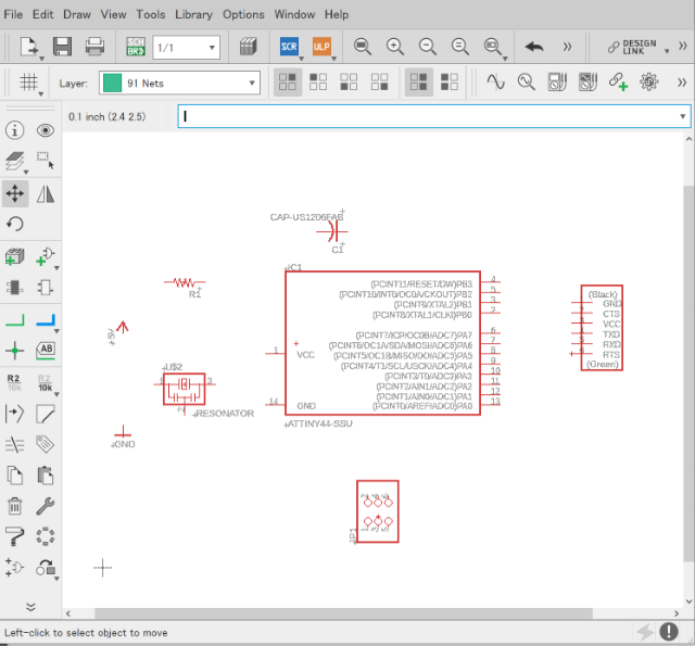
From here, add LEDs and switches
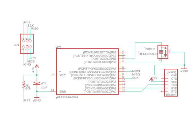
Make the following wiring
- Connect LED to PA7
-
Connect a switch to PA3, and if not pressed with a pull-up resistor, set the voltage to be applied.
-
Add LED & Switch
- The switch has a pull-up resistor so that the normal state is HIGH, and becomes LOW when pressed.
If do not put anything, the state will not be stable. 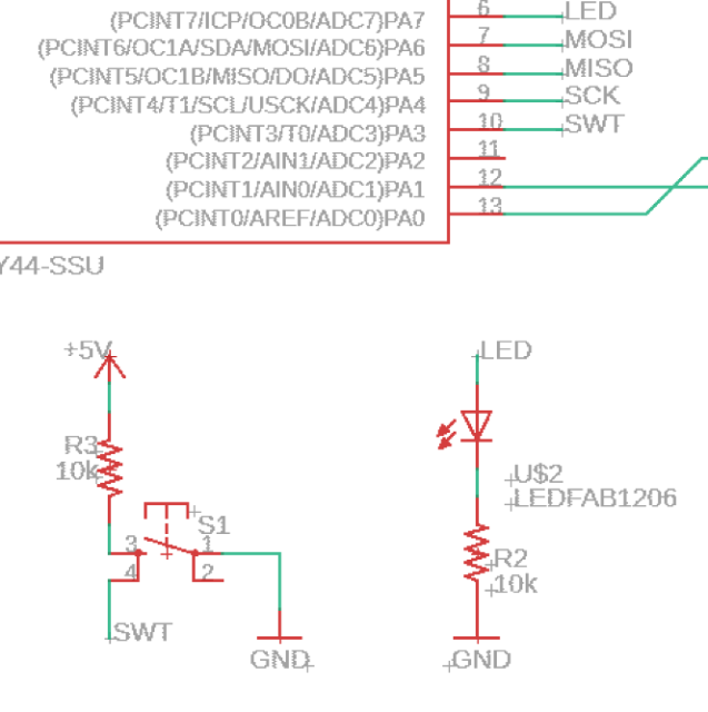
- The switch has a pull-up resistor so that the normal state is HIGH, and becomes LOW when pressed.
-
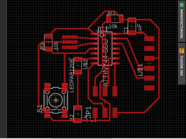
Overall
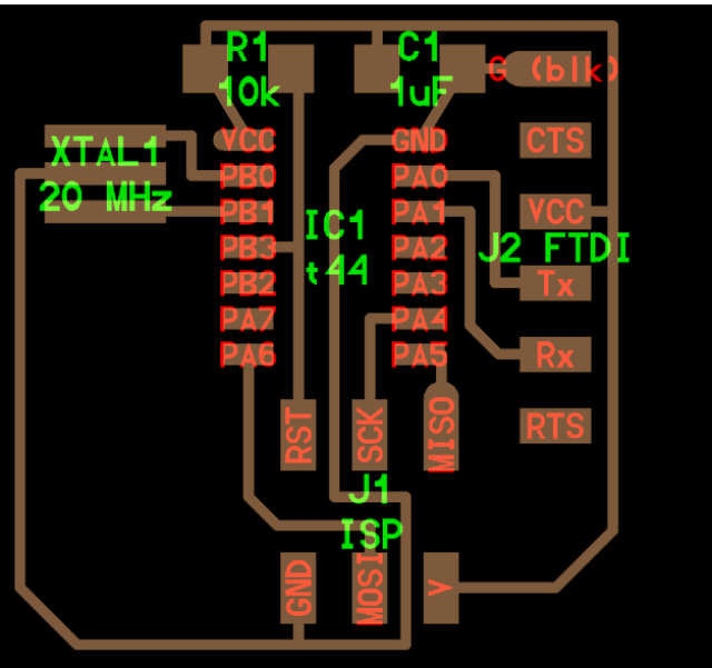
Board Design
-
Switch Board
-
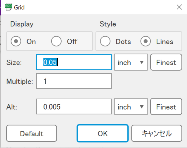
Settings
- Since the grid is not displayed, therefore, make display settings of the grid Draw a line every 0.05 inches
-
It was impossible to wire the switch to PA3
Use the pin on the left according to the location of the switch- Change PA3 to PB3
-
Result
-
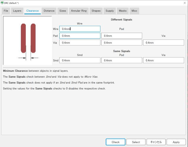
Check DRC
- Perform design rule check
- Change the clearance to 0.4 mm
-
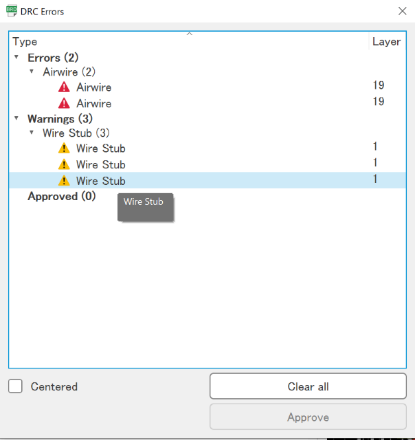
Fix the error
- Air Wire mean not connect
- wire Stab mean overlap
-
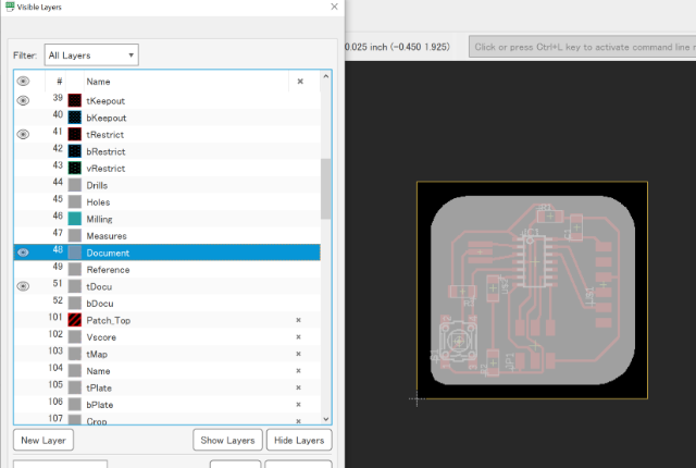
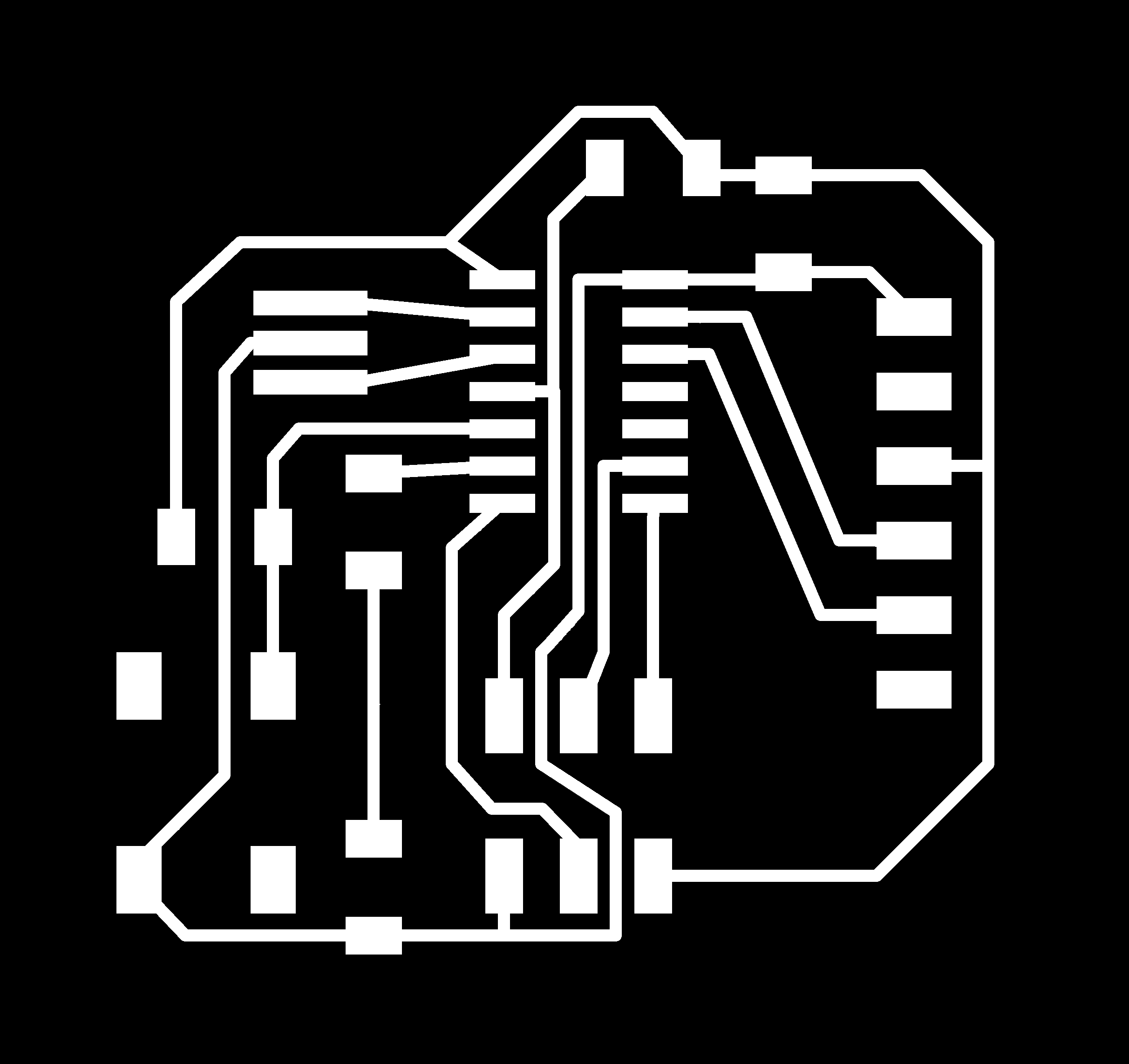
Write Outline
-
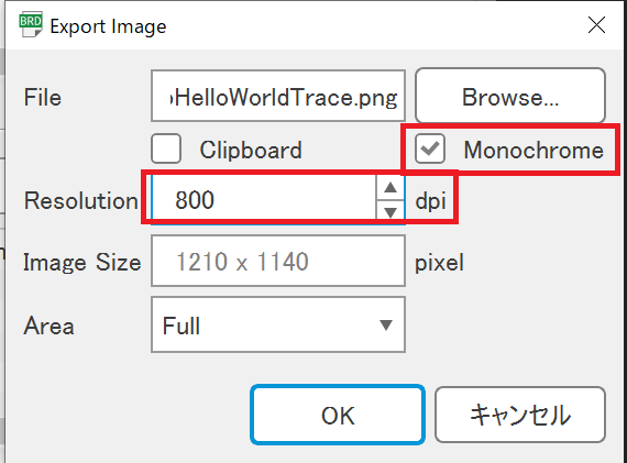
Export
- 800 dpi
- monochrome

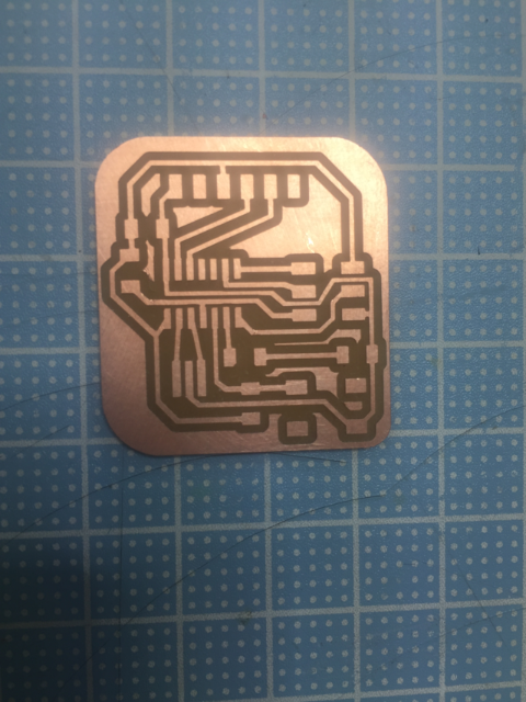
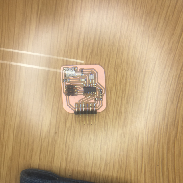
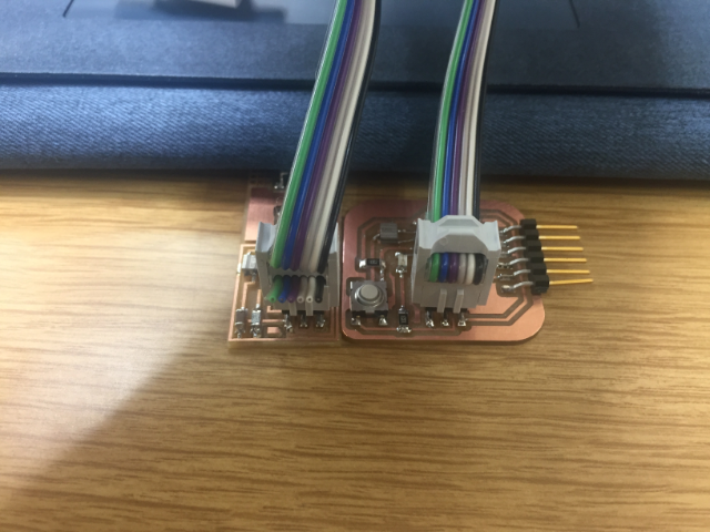
To Cutout
I Cut it like Week 5.
- Cutout
- Line up
- Soldered
- Connect
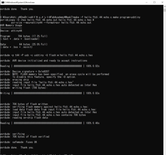
Programming
Using Tool & Software
-
Programmer
- FABISP (created in Week 5)
-
Software for communication
-
Test Programs
-
Commands
-
Communication Test Program
-
FirstCommand
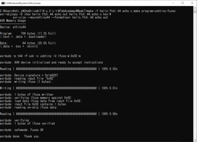
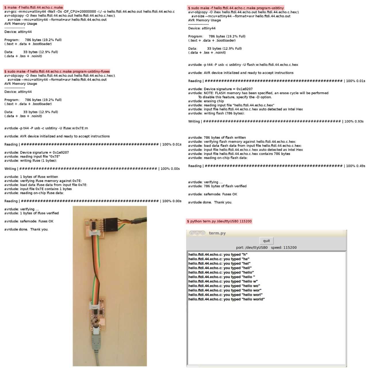
-
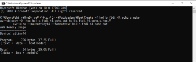
make -f hello.ftdi.44.echo.c.make -
Second Command
-
sudo make -f hello.ftdi.44.echo.c.make program-usbtiny-fuses -
Third Command
sudo make -f hello.ftdi.44.echo.c.make program-usbtiny-
-
Communication Test
-
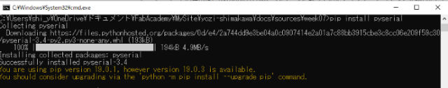
serial is not found
- type “pip install pyserial”
-
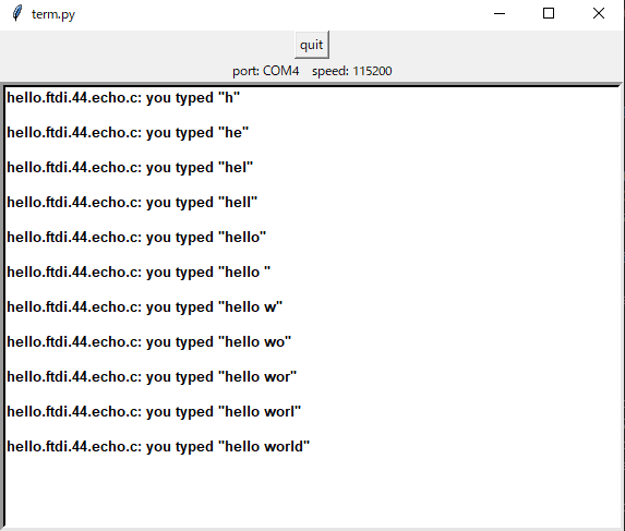
Retry Communication Test * I have been used Python3 but term.py is for Python2.
-
I change term.py for Python3.
-
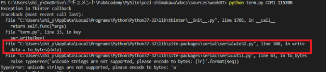
Program not work
- Error in serialwin32.py at line 308
- data was need encode

-
-
Hello world