
Kati Pitkänen @ FAB LAB OULU · 2018
© 2018 Kati Pitkänen · Template by Bootstrapious

This work is licensed under a Creative Commons Attribution-NonCommercial-ShareAlike 4.0 International License.
Electronics Design
Week 7 · [ 28.02.2018 - ]
- Use the test equipment in your lab to observe the operation of a microcontroller circuit board (Group Project)
- Redraw the echo hello-world board, add (at least) a button and LED (with current-limiting resistor), check the design rules, make it (if you have time this week, test it). (Individual Project)
- Optional: Simulate its operation. Measure its operation.
This week involved in a lot of learning. Partially it came by trials and errors, partially because of exploring and forming an understanding of many things connected to the topic of the week but new for me. Many thanks to our local instructor Antti Mäntyniemi for his guidance and great willingness to share his excitement in the world of electronics.
During the week I revised myself of drawing schematics and boards, setting the design rules, creating files to mill, and set up the milling machine. Last time, when producing electronics on the week 5, I did better but this time my soldering process was not too successful so, I need really to practice that. Later on I found, that I should have used smaller soldering head to get better results. However, I learned about Resistor SMD coding and familiarized myself with the four-digit system. Also, since I faced short circuits after assembling the board left by the milling machine, next time I will be trained to be more sharp-eyed to recognize those right after the milling. Further, observing the operation of a microcontroller circuit board with the oscilloscope, and simulating its processes with Tinkerdac Circuits.io was interesting.
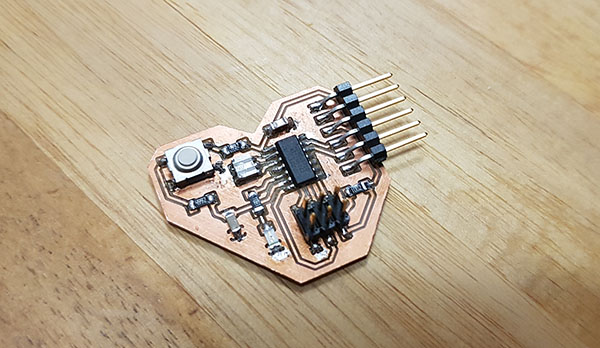
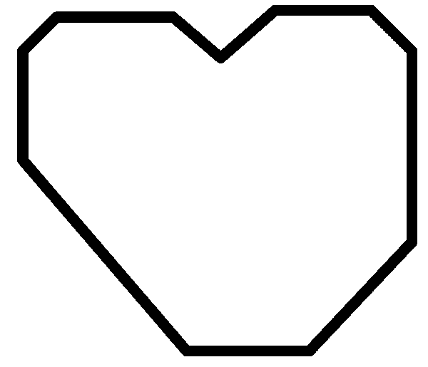
Redrawing the Echo Hello-World board
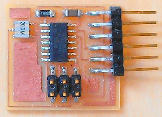
I used Autodesk Eagle 8.6.3 to redraw the Schematic and Board Layout of Echo Hello-World board. In order to learn to identify the components, I redesigned and redraw the components to a schematic by looking at the picture of the assembled board and the board layout:
First of all, download the fab.lbr -component library by right-clicking 'Save the link' and adding the library to Eagle installation folder (C:\EAGLE 8.6.3\lbr). Then, open the Eagle and navigate to Libraries > lbr where you can see the new library marked with the grey small dot. Activate the library by right-clicking it and selecting "Use".
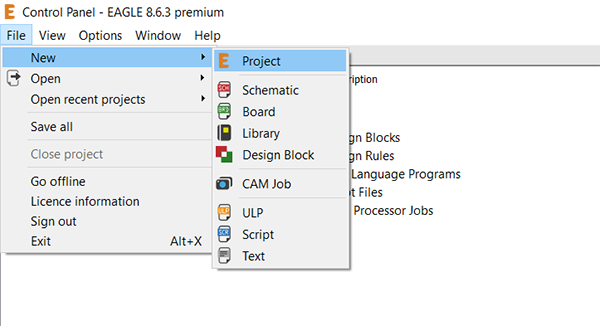
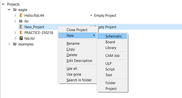
Next, I created a new project by navigating File > New > Project. Then, I created a new schematic by right-clicking the New Project > New > Schematic.
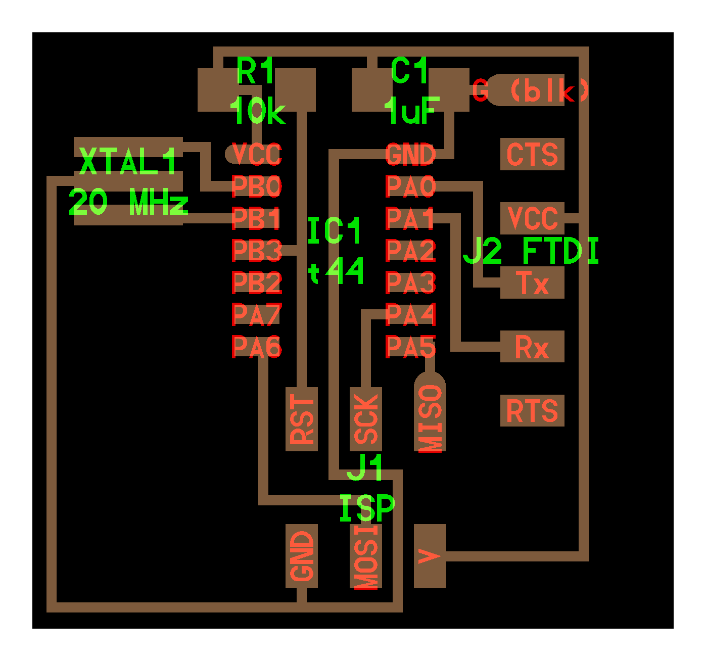
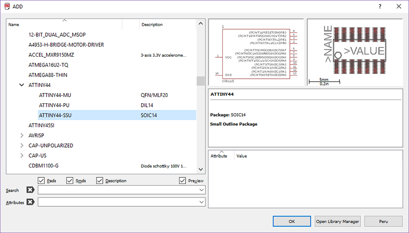
In the schematic, I searched all of the components by 'Add' -tool and placed them nearby where they were going to be located. For the original Echo Helo-World Board, based on his experience Antti Mäntyniemi suggested to add a filter for the pushbutton to avoid unexpected glitches when releasing the button. In order to avoid this, he suggested to use a filter consisting of two resistors and a capacitor to make the falling and rising signal of pushbutton solid.
From the fab -library I added:
From the same library, I added a button and a red LED with a current-limiting resistor to the board.
From the supply1 -library I added:
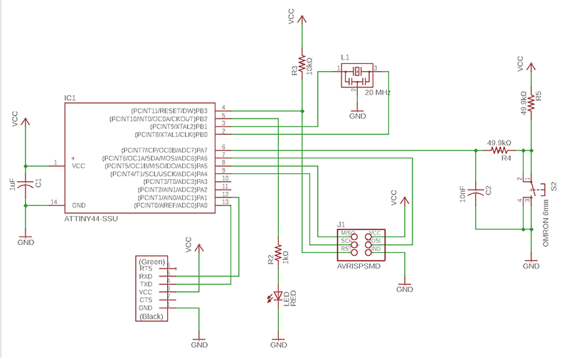
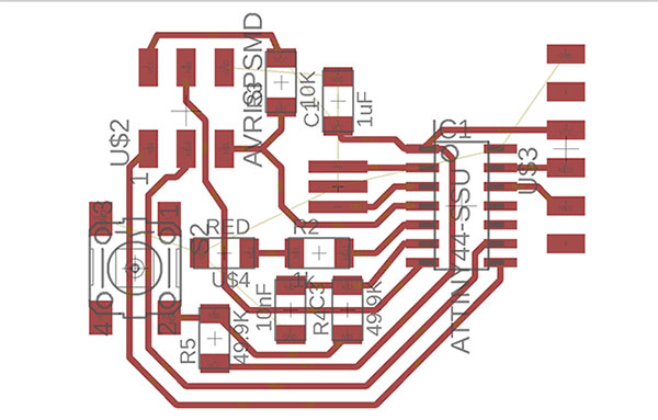
After adding all of the components, with the help of ATtiny44A datasheet, where I was checking the pin numbers of the microcontroller, I started to arrange and place them in their final locations:
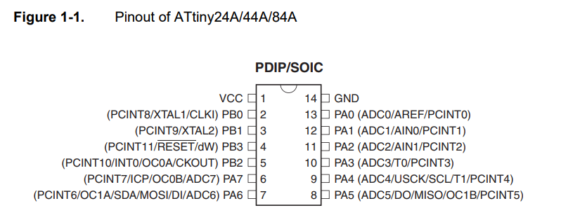
- ATtiny44A microcontroller // to the center of everything
- Pin header 2x3 // nearby the microcontroller's:
- pin 7 // connecting to header's MOSI (Master Out --> Slave In)
- pin 8 // connecting to MISO (Master In --> Slave Out)
- pin 9 // connecting to SCK (Serial Clock)
- pin 4 // connecting to RST (Reset) and
- resistor R3 of value 10 kΩ
- + add VCC and GND components next to them.
- Pin header 1x6 // nearby the microcontroller's:
- pin 12 // connecting to header's RXD, and
- pin 13 // connecting to TXD
- + VCC and GND next to them.
- Capacitor C1 of value 1 uF // in the middle of microcontroller's pin 1: VCC and pin 14: GND + VCC and GND
- Capacitor C2 of value 10 nF, and two resistors R4 and R5 of value 49.9 kΩ // together with the button OMRON 6mm, connecting to the pin 6 + VCC and GND
- Resonator R1 of value 20 MHz // nearby the microcontroller's pin 2 and pin 3
- Red LED // connecting to microcontroller's pin 5 through resistor R2 of value 1 kΩ in between them + GND
Then, I wired the components using the Net -tool.
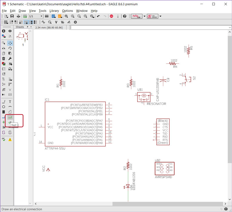
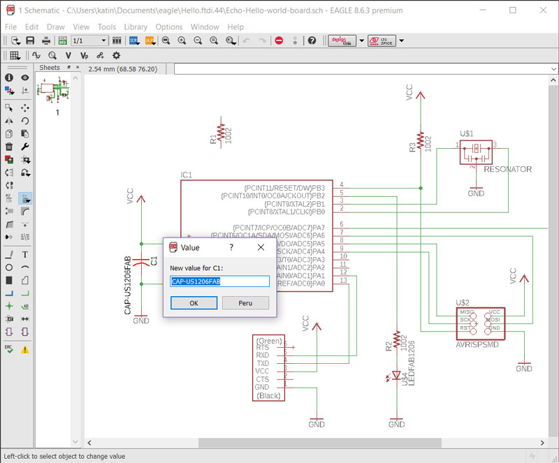
By right-clicking above the component and selecting Properties I named the components and gave them correct value. For some of the components, I had to give the correct value by selecting Value.
I moved to Board Layout by navigating into the top bar and taking Generate/Switch to board button for drawing the traces for the circuit.
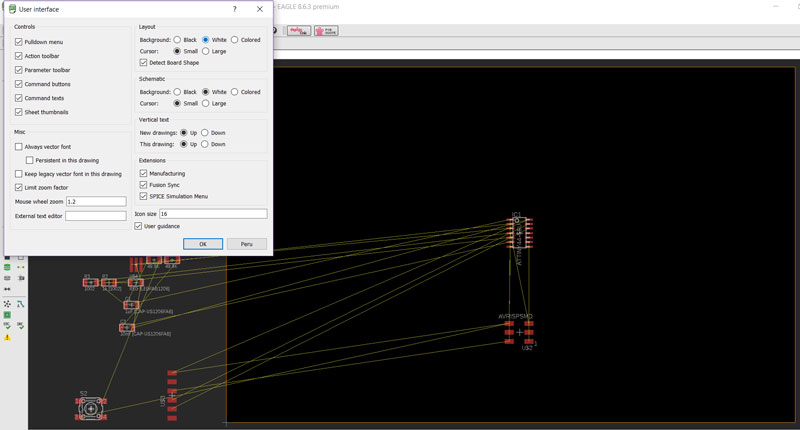
I prefer more light so I changed the black background to be white by navigating in the top bar Options > User interface > Layout.
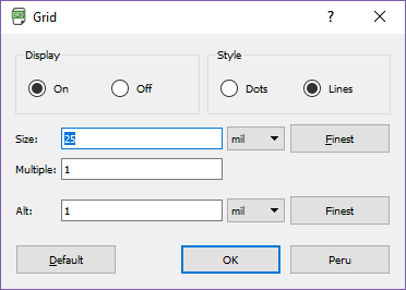
In order to align and move components freely, by navigating in the top bar, select Grid tool. Set Display ON, and Size to be e.g. 25 mils, and Alt to be 1 mil.
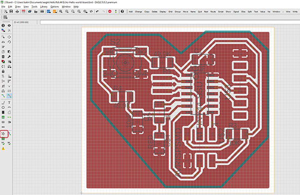
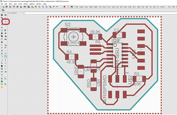
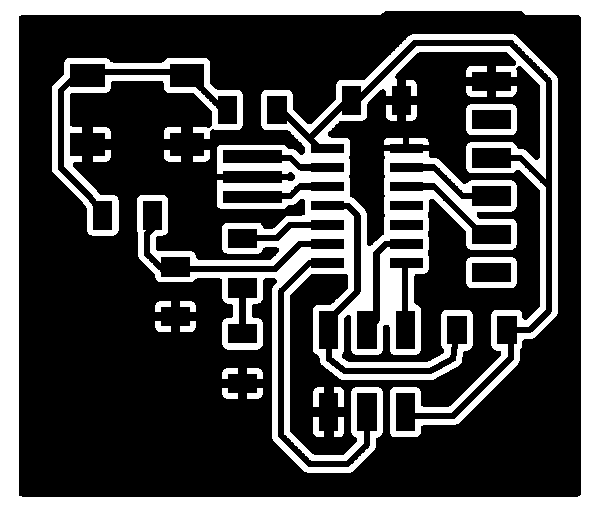
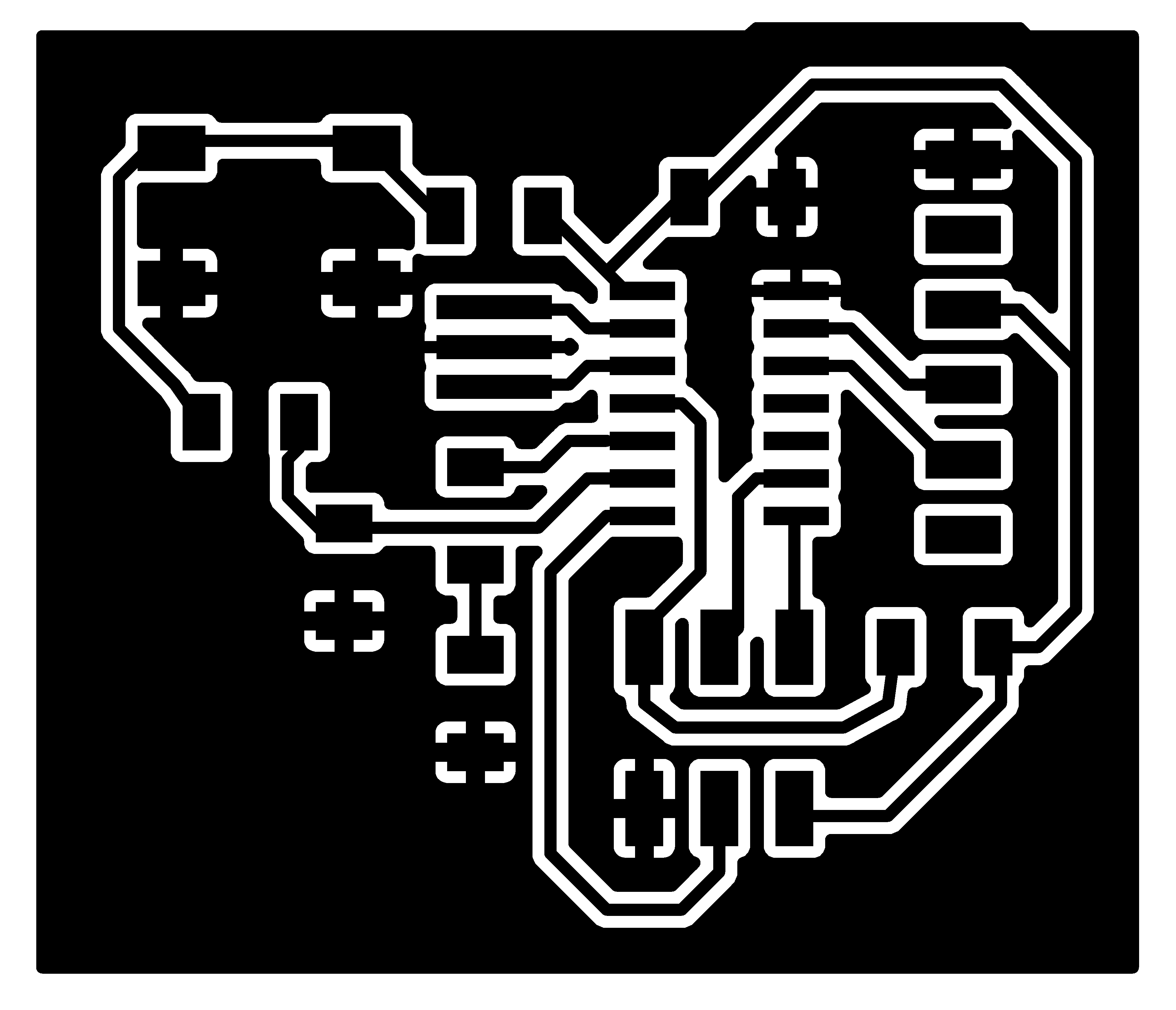
The first trial was a failure. In short: I started to organize the components by moving ATtiny44 microcontroller to the Dimension -area and continuing to move the other components around it in groups belonging together. Then, I thought about the use of the board. I wanted the pin headers to be in logical orientation so that user doesn't have to think about in which orientation the cables should be connected but it would be obvious. This is why I placed the two pin headers on opposite sides of the board and continued by placing the rest of the components around them. I could see, that because of placing the pin headers like this, the wires were going to be quite long and serpentine. I thought, why not forming them a bit when they anyway will be "too long", and I placed them in the shape of the heart.
I selected the Route -tool, and in the top bar, I set the wire width to be 16 mils, and then created the copper wires manually. Every now and then, after replacing the components, by the Ratsnest -tool, I rearranged the connecting airwires for seeing better, which components should be still connected.
When trying to fix the mistake of non-grounded areas, in order to see better the working area, from the top bar I navigated to Options > Set > Misc, and removed the 'Display pad names', 'signal names on pads', and 'signal names on traces'.
Also, I checked from the schematic by the Show -tool that I had added all of the needed GND -components.
However, I failed for two reasons:
I tried to modify the board but I found that it was a better idea to make it all over again.
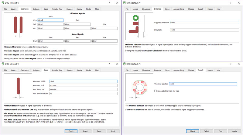
For the second trial, I tried to follow carefully the design rules of drawing a PCB board. Starting from the settings, I did as follows:
Selecting the DRC (Design Rule Check) settings from the toolbar, I defined new values:
- Clearance // set all the 'Different Signals' and 'Same Signal' to be 16mil
- Distance // set Drill/Hole to be 16mil
- Sizes // set Minimum Widht to be 16mil, too
- Supply -tab // set 'Thermal isolation' to be 10mil, and 'Apply'
Using Move -tool, I placed all of the components to the Dimension -area. Again, I placed ATtiny44 microcontroller in the center, and Capacitor C1 1 uF above it next to VCC and GND and continued by grouping rest of the components. I didn't make a too tight package in the beginning but placed the components' legs, which were supposed to be connected, next to each other. The aim is to make the wires go from leg to another as short and straight as possible so, by Rotate -tool I rotated them to be in the appropriate orientation on the board. The first placing I did very wide.
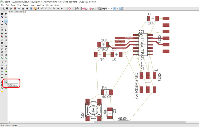
Then, I selected Autorouter -tool, and did Autorouter Main Setup where, outside of the Top -layer, I set the Preferred Directions to be N/A', and pressed Continue, and Start. From the Routing Variants Dialog I was able to see if there was any successful routing possibilities based on the placing and orientation that I had done.
If there was any Completed Optimize': 100% option I continued from that one, and by 'End Job' I saved the routes and returned to modify and develop the board layout to be tighter and wire lengths minimized. By typing to the command line "ripup;", I could remove all of the wires again, and start to replace and wire or autoroute them from the beginning again. By using the Ripup -tool, I could remove wires one by one.
After several iterations, I was satisfied with the result. (It just happened to be in the form of heart again.) By the Route -tool I fixed manually the wires. I removed all the 90-degree angles and made the wires look aesthetically nice.
In order to check that there are good connections and enough ground around the components without any islands of the non-grounded area, I created a ground layer:
- In the left toolbar, select Layer settings and add layer no 46 Milling to Visible Layers.
- Moreover, in the left toolbar, click on the Line -tool, and then from the top bar, Select layer: 46 Milling and line Width: 40 mm.
- Now, on the Milling -layer, draw board outline that will be marked with a turquoise line.
- Then, in the top bar, select the Dimension layer. By grapping and dragging, crop the Dimension layer to fit in the size of the board outline, marked with a thin orange line.
- Select the Top layer again, and using the Polygon -tool, follow the inner edges of Dimension, and create a line marked with a red dotted line (double click to accept the border) to be a ground border.
- FInally, by right-clicking above the ground border, I selected Name, and gave New name: "GND" for it, and hit OK.
Using the Ratsnest -tool, I made sure that the ground reached the ground pads of components. At this mode, I adjusted placing of components in order to get rid of too thin spaces between the wires and non-grounded areas. Also, I finished modifying the outline borders.
Things to remember:
Change the width of tools for every tool separately, e.g. when using 'Route' for wiring or 'Line' for creating an outline. I had not done that at first for the milling layer so, I had to do it at the end by right-clicking above the milling outline > Properties > Width 40.
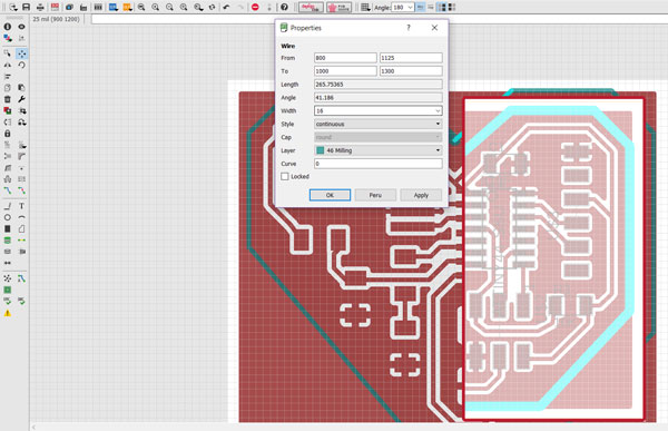
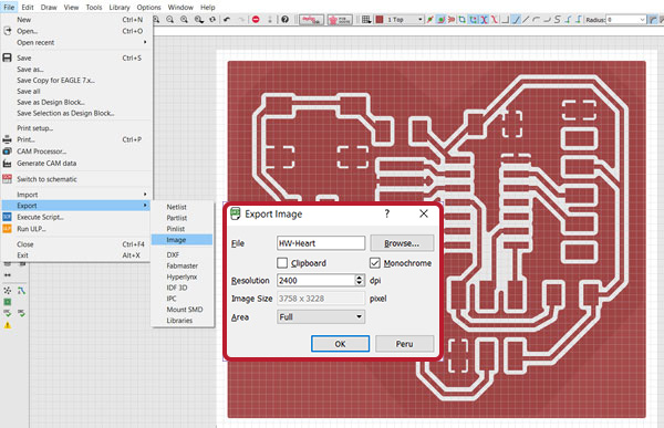
When the board layout is finished, select Layers and leave only the Top layer visible.
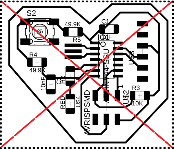
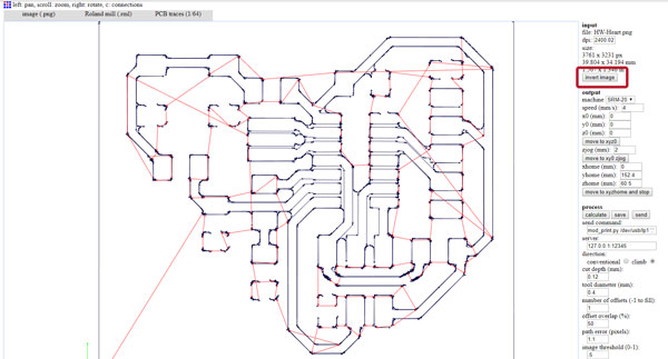
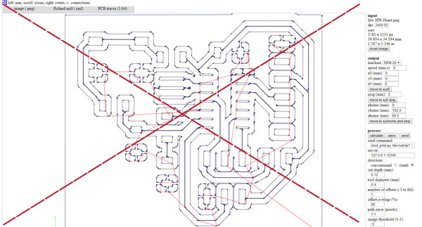
Otherwise, the .png will look incorrect (the first picture). After only the 'Top' layer is selected, navigate File > Export > Image.
Name the file, select Monochrome and define Resolution: 2400 in order to reduce rounding error.
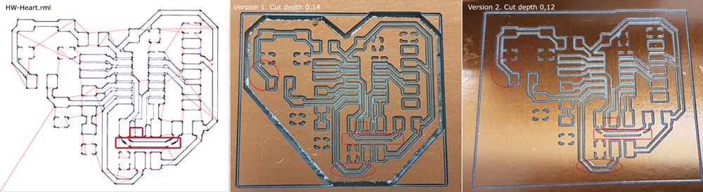
Fabmodules.org to get .rml -files
Creating the .rml files in Fabmodules.org by the process documented during the Week 5. (As Bas suggested, next time I will try Mods.)
When designing the board with the white background, Export > Image causes one extra step to remember: either in changing the background for a moment in Eagle or inverting the picture before calculating and creating an .rml -file in fabmodules.org in order to get correct result (the first picture), or otherwise you will see how the routes after calculation look very weird when all the black in the picture would be cut away (the second picture).
Milling the PCB
I prepared the Roland SRM-20 milling machine based on the documentation I did on the Week 5: Preparing the milling machine Roland SRM-20 and milled the board based on the documentation of the same week: Milling PCB via Fab Modules.
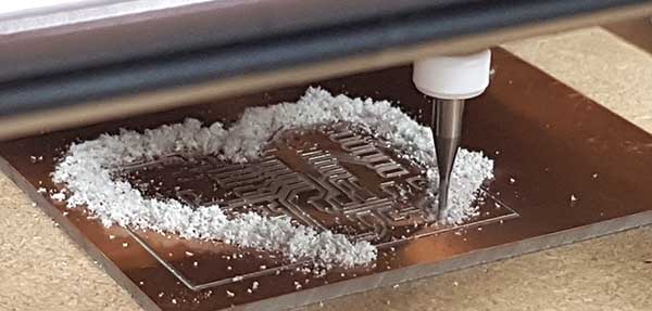
I had to do the milling twice, and for the second one I made a change in the cut depth. In the first board, the cut depth was 0,14 mm and in the second one 0,12 mm. The difference can be seen clearly when comparing the pictures below. The change was because the milling bit seemed to cut so deep that the wires got quite narrow. Another problem (occurring in both boards) is that for some reason, the cutting lines calculated in fabmdules.org didn't meet in the middle of the pin header 2x3 so, I had to remove the piece of copper in order to avoid short circuit. For some reason, I didn't recognize from the second board that because of rising the milling bit slightly the cut of the middle pad for the pin header didn't cut through but left a tiny bridge of copper - enough to create a short circuit, which was found by testing with the multimeter.
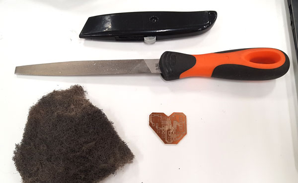
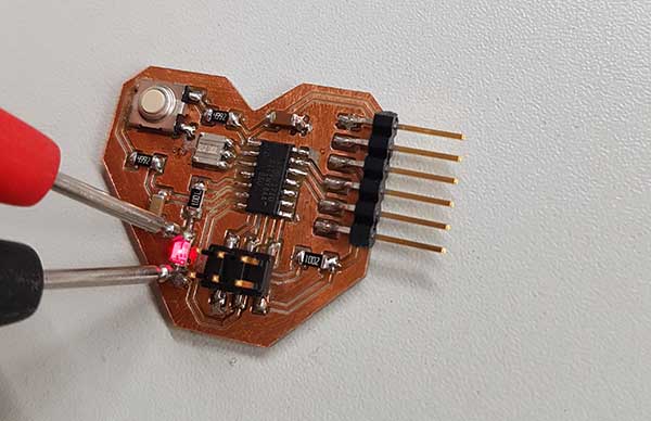
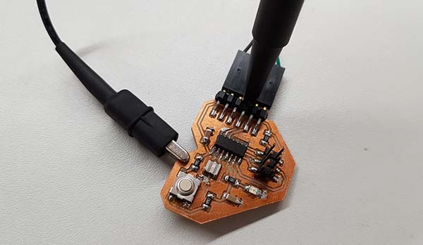
Assembling the Components
I followed the instructions got and documented during the Week 5 in the soldering process. This time I am not satisfied with my result in soldering so, I have to practice it a lot. However, it was a good practice to experience soldering in these narrow and tight conditions.
I collected all the necessary components and like on the Week 5, labeled them to a sheet of paper attached by tape, making easy to recognize the components and see the whole, and pick up the right component during the assembling process:
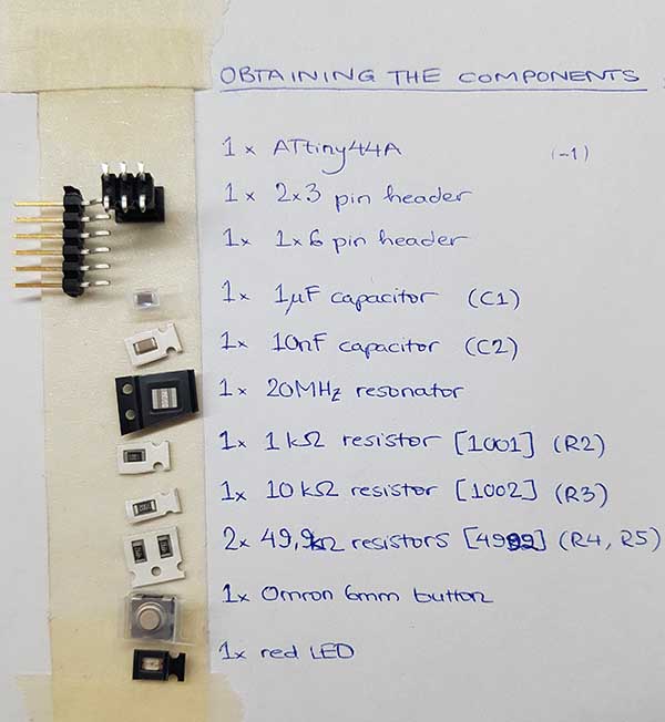
- 1x ATtiny44A microcontroller
- 1x 2x3 Pin header
- 1x 1x6 Pin header
- 1x 1 uF Capacitor (C1)
- 1x 10 nF Capacitor (C2)
- 1x 20 MHz Resonator (R1)
- 1x 1 kΩ Resistor [1001] (R2)
- 1x 10 kΩ Resistor [1002] (R3)
- 2x 49,9 Ω Resistors [49R9] (R4, R5)
- 1x Omron 6mm Button
- 1x red LED
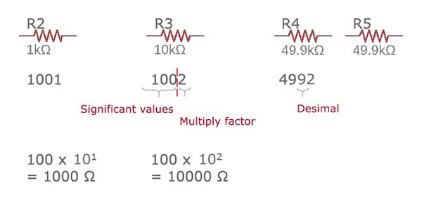
I learned about Resistor SMD coding here and here.
In the four-digit system, the first three numbers indicate the significant values, and the fourth number is a multiplying factor.
- Therefore, an SMD resistor with the figures 1001 would have a resistance of 100 x 10 to the power of 1 (ohms), being 1000Ω or 1kΩ (ohm).
- Thinking the opposite, an SMD resistor with the resistance of 10kΩ or 10000Ω, would be 100 x 10 to the power of 2 (ohms), being marked with the figures 1002.
The R represents a decimal meaning, that resistors with values of less than 100Ω are marked by the letter 'R' to indicate the position of the decimal point.
- An SMD resistor with the resistance of 49,9kΩ would be then marked with the 49R9.
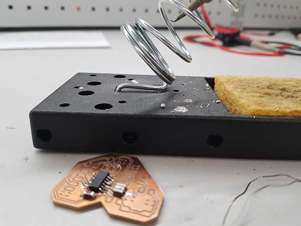
Testing the Echo Hello-World board
I tested continuity using multimeter in order to check that connections are fine, and find possible unconnected circuits or short circuits. I set the multimeter to "continuity and diode test" and followed circuits from pins to and aroud the components to see, if the connection is fine. Multimeter gives a sound every time the probes are connected through circuit which is a good sign if there should be connection, and very bad if there shouldn't be but the multimeter finds one meaning that there is a short circuit, or if the device keeps silent even there should be a connection meaning that it is broken (e.g. the leg of component is not well soldered but in the air).
I wasn't experienced and careful enough in ocular estimating and testing to find the mistake I found later on when I tried to program my board unsuccesfully. The problem was the short cut under the 2x3 pin header, which we found with my fellow student Ari by testing the board again with multimeter. It wasn't simple to move that short cut carefully under the component but finally, by breaking the extra copper piece with thin sharp object, the board worked perfect and became programmable.
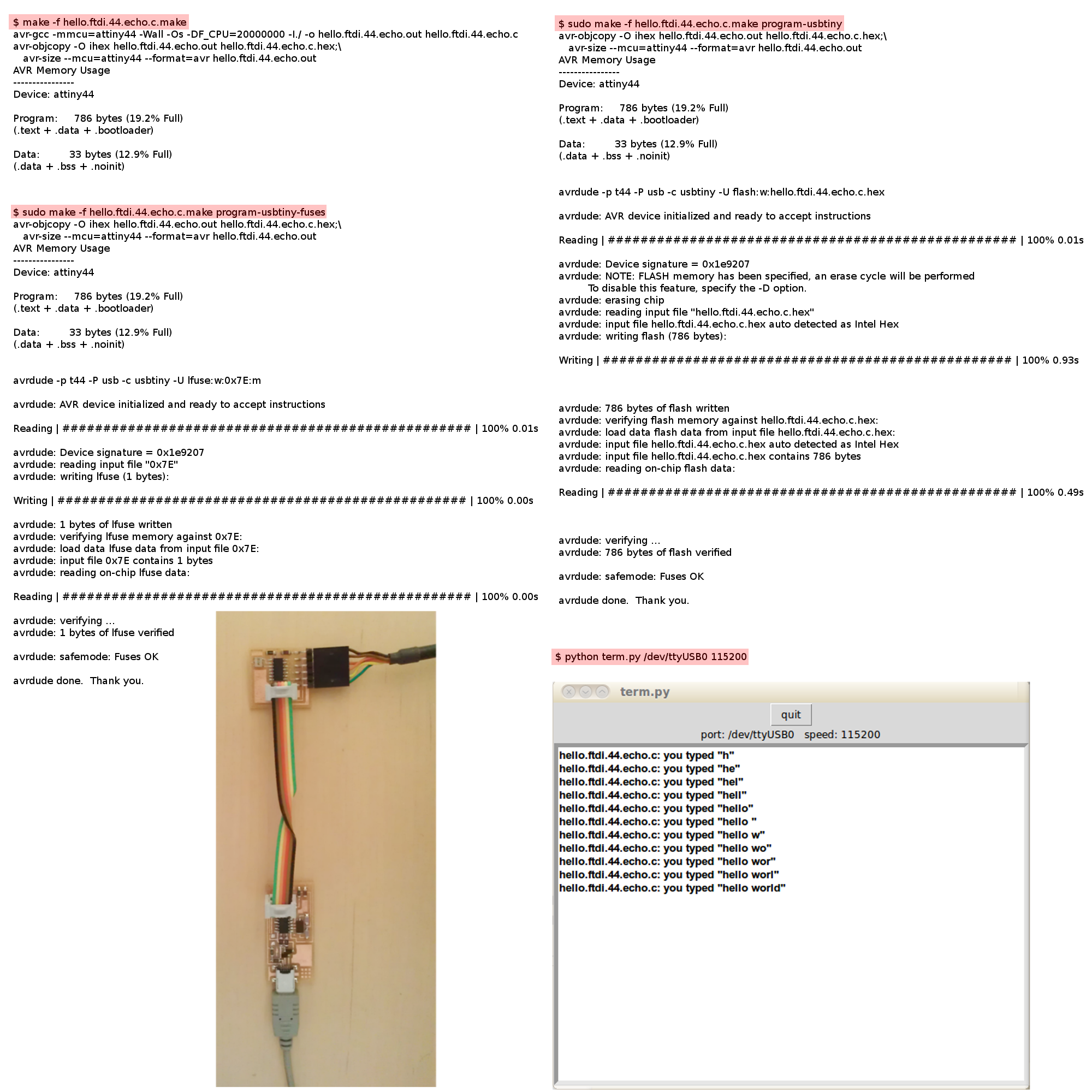
Programming the Echo Hello-World board
Programmed following the instructions. (Note: 'sudo' is for Linux only.)
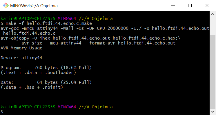
First of all, I compiled the codes:
make -f hello.ftdi.44.echo.c.make
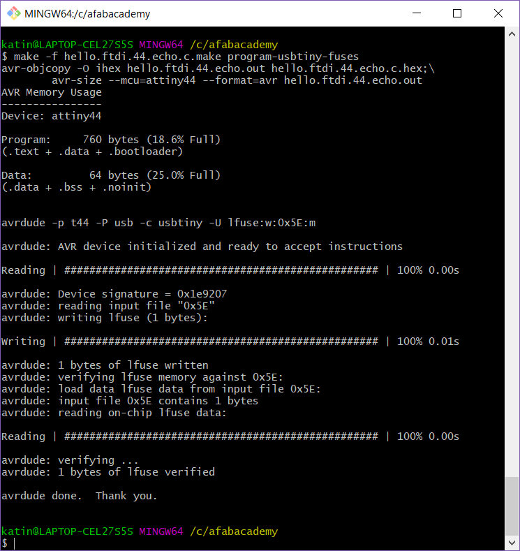
Next, I set up the microcontroller for programming:
make -f hello.ftdi.44.echo.c.make program-ubtiny-fuses
And then, I flashed the program to microcontroller's memory.
make -f hello.ftdi.44.echo.c.make program-usbtiny
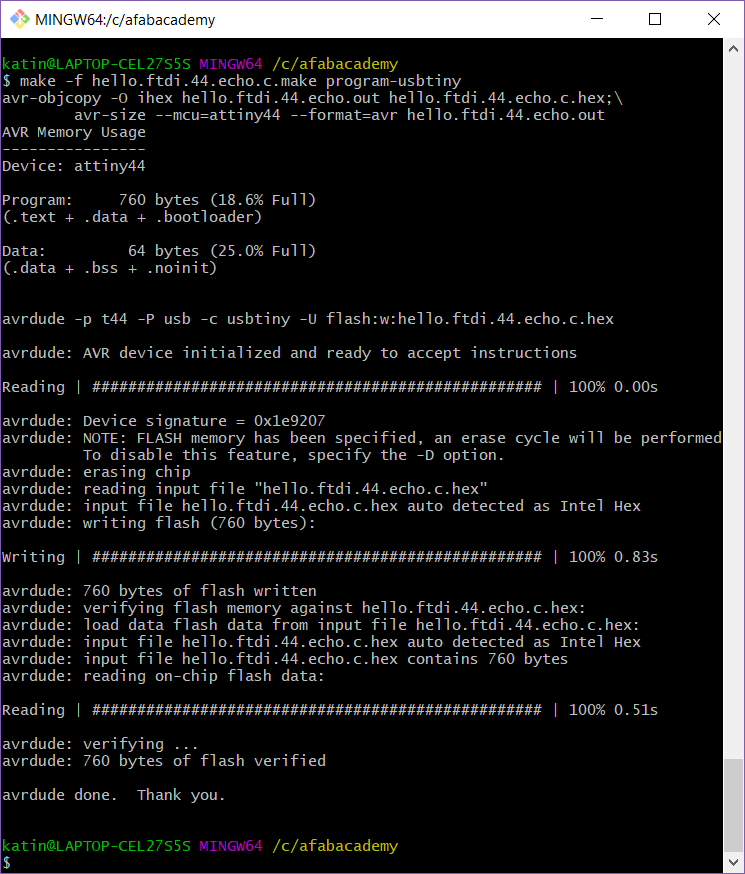
Now, the programmer can be removed and only the programmed board needs to be connected through FTDI -cable.
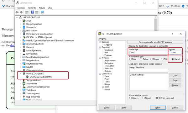
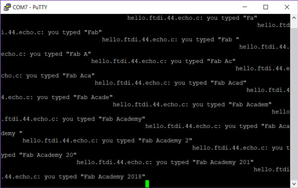
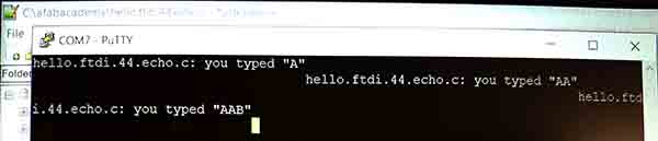
I was not familiar with Python and I had some challenges in downloading and setting it up so, I moved to try with PuTTY terminal to see, if my programming works. I downloaded and ran the 'MSI (‘Windows Installer’)' and opened the software to make PuTTY Configuration:
- Connection type // Serial
- Serial line // The USB port the board is connected [COM7]
- Speed // 115200 (baud rate)
And hit 'Open'.
Fortunately, after having challenges with terminals, everything worked just fine!
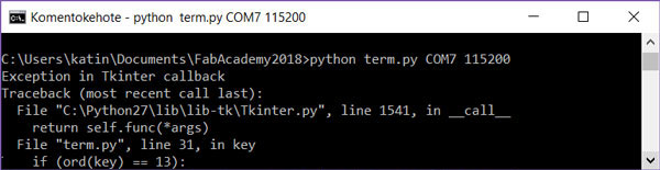
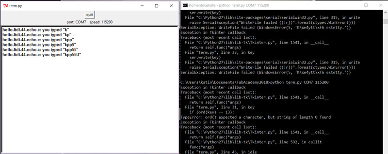
Then, I still didn't want to give up but continued with Python. The first version I installed was Python 3.6.4, but I had challenges with term.py (and Tkinter.py) so, I was suggested to change for Python 2.7, which I installed succesfully.
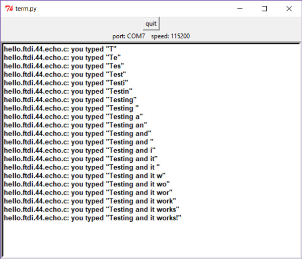
Finally, for opening the terminal, I used a command 'python term.py /dev/ttyUSB 115200' (where /dev/ttyUSB means the USB -port the programmer is connected)
and it worked!!
python term.py / COM7 115200
Many thanks for the great help to get started in this new area for our local instructor
Iván Sánchez Milara
and my fellow students Marta Cortes Orduna and
Ari Vuokila.
Observing the operation of a microcontroller circuit board
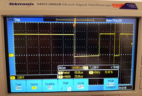
This week alongside of designing electronics, we tested equipment in our lab to observe the operation of a microcontroller circuit board measuring the operations of a pushbutton with and without a filter with oscilloscope. Without the filter, the resistance was going to the button through one 10 k ohm resistor only. With the filter, the resistance was going through two 10 k ohm resistors and a 10 nF capacitor, too.
when observing how the filter operates using Antti's example board and jumper to connect and unconnect the circuits, the following pictures are showing how the pushbutton without a filter (having only pull-up resistor) affects glitches when it is released, where the pushbutton with a jumper gives clean signal without glitching.
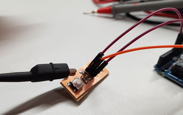
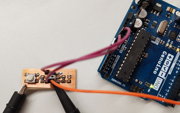
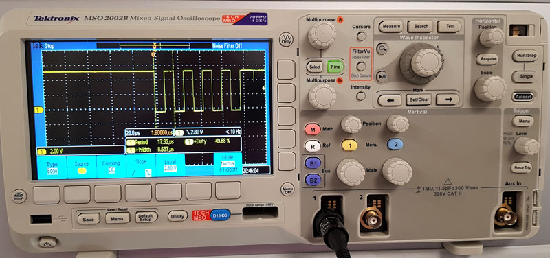
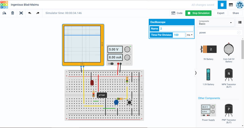
Then, I wanted to understand better the operations and learn to use oscillator so with Antti I observed some basic operations of my own board.
I connected oscillator probes to my Heart board, one to ground and another one to the pin 13 [TxD], and opened a command window and PuTTY terminal.
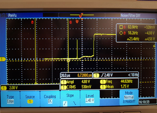
I measured the bit speed and width of one pulse received from the microcontroller when pressing the key in the keyboard, by sending letters capital A, capital, A and capital B from my laptop keyboard to the board, and measuring the outcome:
As it can be seen in the picture, that the frequency of the pulse is 114 kHz // ~ 115 khZ = ~115200 Hz
- [ Frequency F = 1/T (s) ] = 1/8,68 us // (bits per second, equal to the number of bits transmitted or received each second)
Thus, the width of one pulse is 8,637 us (microseconds)
- [T = 1/F (Hz) => 1/115200 = 0,0000086806 s]
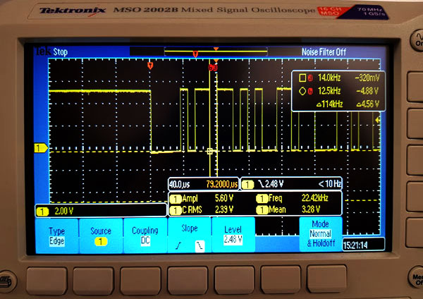
Typing " p ", writes bit serie 0000 1110
- which I will read starting from the least significant bit (LSB) to the most significant bit (MSB) to get the bytes correct 0111 0000
- being "70" [0+1+1+1 0+0+0+0],
- (which in ASCII -table is lower case p).
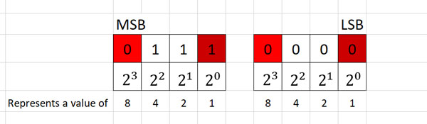
In computing, the least significant bit (LSB) is the bit position in a binary integer giving the units value. The convention in positional notation is to write the less significant digits further to the right. This is analogous to the least significant digit of a decimal integer, which is the digit in the right-most position.
(There, in an 8-bit binary number, MSB represents a value of 128 decimal, and the LSB represents a value of 1.)
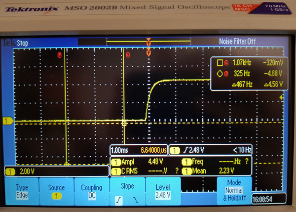
Typing " U ", writes bits 1010 1010
- which will give me 0101 0101
- being "55" [0+6+2+1 0+6+2+1],
- (which in ASCII -table is capital U).
The width of one pulse is 8,637 us.
Simulating
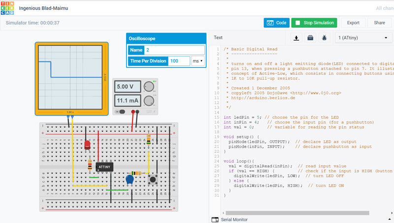
Lastly, I simulated the operations of the The Heart Shaped Echo Hello-World board by Tinkerdac Circuits.io, when the pushbutton was pressed and released to turn the LED On and OFF.
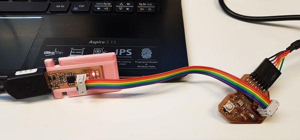
Cable for Programmer
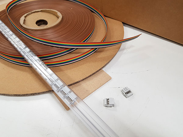
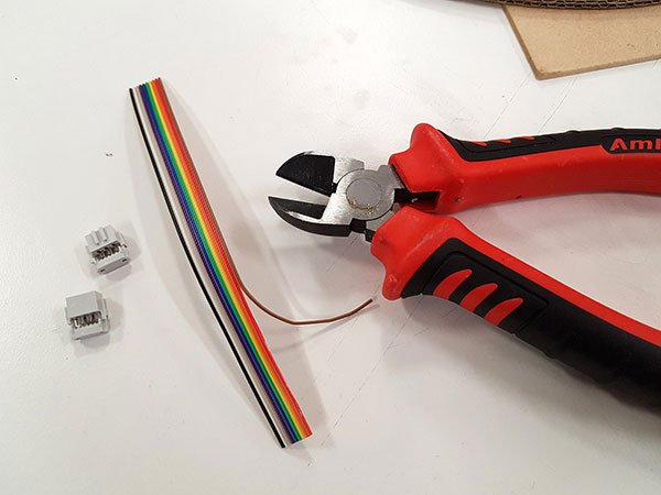
I produced a cable for my programmer last week, because I wanted to 3D design and -print a cover for my programmer. For that, I needed to take the measurements of the cable attached on the programmer.
For making a cable, I needed:
- 1 x 9-way ribbon cable in a length I considered appropriate, where I removed three extra lines, and
- 2 x SPI headers.
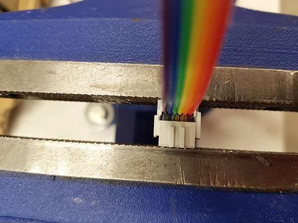
I placed the cable inside the header and checked carefully that the orientation is fine. For closing the header I utilized a table clamp but I had to be careful and fasten very gently the header for avoiding to break it.

Here are the design files of The Heart Shaped Echo Hello-World board I made this week.