
Kati Pitkänen @ FAB LAB OULU · 2018
© 2018 Kati Pitkänen · Template by Bootstrapious

This work is licensed under a Creative Commons Attribution-NonCommercial-ShareAlike 4.0 International License.
Electronics Production
Week 5 · [ 14.02.2018 - ]
- Characterize the specifications of your PCB production process (Group Project)
- Make an in-circuit programmer by milling the PCB (program it, so that you can use it to program your board in Electronics Design week, and in other weeks) (Individual Project)
- Optionally, trying other processes.
This page describes my learning process to mill, stuff, de-bug and program the PCB (printed circuit board). I had done only a couple of PCB:s beforehand and a very little soldering so, this week involved in a great place to develop my understanding of the PCB:s, recognizing some basic components and practice soldering. Many thanks to our local instructor Jari Pakarinen for his eager way to guide us through the week.
I really enjoyed the assignments and soldering, and there were no big challenges during the week. However, I need to practice soldering to make my joints beautiful.
Making an in-circuit programmer 'FabTinyISP'
Basically, PCB is a board, which is used for mechanically support and electrically connect electronic components forming an electrical circuit, physically consisting of different layers laminated together.
The FabTinyISP is Brian's version of an AVR ISP programmer/board which one I chose in order to produce a milled PCB and some basic components. As Brian describes, this programmer is based on the efforts of several people, and the ones who have contributed to it in addition to him, can be found Zaerc's FabTinyStar page.
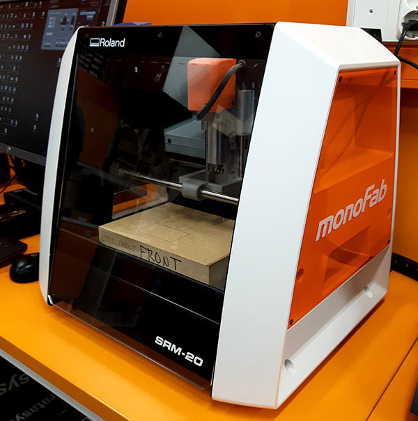
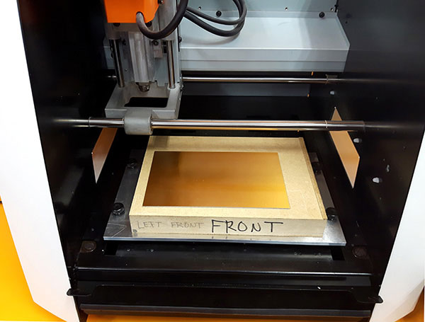
Preparing the milling machine Roland SRM-20
For milling I used Roland SRM-20 Desktop Milling Machine.
To prepare the machine for milling, first or all, a PCB has to be placed:
- Open the door of the machine and remove the ground plate by loosening the four screws.
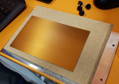
- Take the PCB - in Fab Lab Oulu we have FR-1 which has light sensitive coating - and remove the black tape above it.
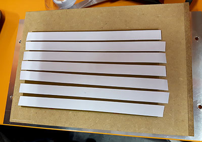
- Turn the board upside-down to see the background and put double-sided tape stripes carefully above it. This is a crucial part and they cannot overlap at all since otherwise the board will be bended. Cut the extra tape off from the sides and clean the board.
- Check the surface of the plate, which has to be absolutely straight and level.
- Put the plate back inside the milling machine right way up and fasten with the four screws.
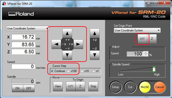
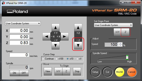
Open the program ‘VPanel for SRM-20' and set the origin of Z-, X- and Y-axes:
- Move the head to the View position so that it moves to the center and it is easier to install a milling bit.
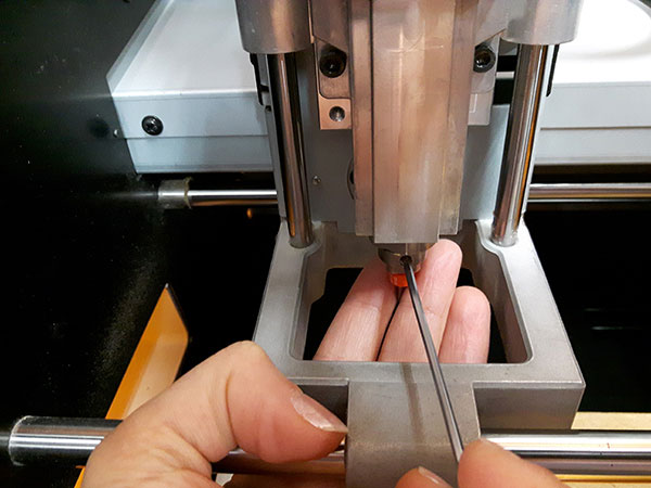
- Loosen the small screw in the shank by allen key, put the orange v-shaped milling bit (size 0,2-0,5 mm) in all the way up to colored neck, and slightly fasten the small screw to fix it. [The grey milling bits in the picture are flat bits.]
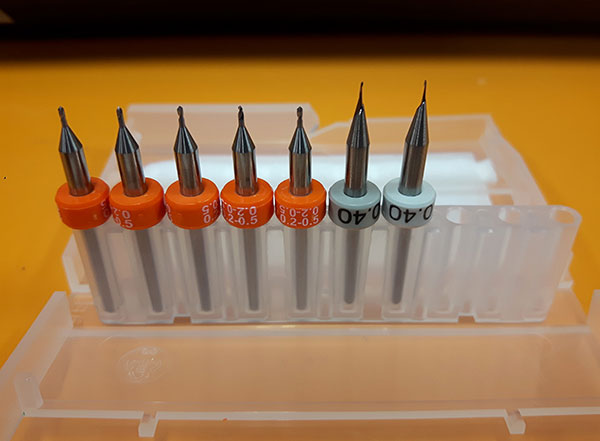
Our instructor Jari Pakarinen described us the differences between a flat milling bit and a v-shaped milling bit. The flat one has told to be very good quality but breaking very easily so, I decided to use a v-shaped one which is also a good milling bit. However, the difference in using them is in the set of cut depth. When milling with v-shaped bit the cut width varies based on how deep the 'Cut depth' is set.
- X- axis moves the table, and and Y- and Z-axes move the head.
- Move the axes manually by the VPanel arrows with appropriate Cursor Step.
- Continue moves as long as you push it, by which you will move near to the aimed origin.
- x100 does smaller steps to get closer and
- x10 0,1 mm steps to get nearby the surface.
First of all, move the Z-head carefully near to the surface.
Adjust X- and Y-axes (with the Cursor Step: Continue, and x100) and reset them to be a new origin by Set Origin Point and pressing X/Y.
Hold the milling bit with one hand, loose the screw with another, and move the bit right on the surface of the board, and then keep the milling bit still so it can't move up when fastening the screw again. Remember to not tighten too much in order to avoid ruin the milling bit body surface.
Now, reset the Z-axis to be zero by Set Origin Point and pressing Z. In order to let the milling bit turn on and speed up freely, move the Z-axis just a little bit up (around 5 steps with the x10) so, don’t leave the milling bit to the surface. Now, the machine preparation is done.

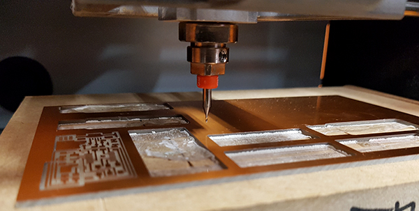
Milling PCB via Fab Modules
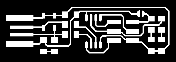
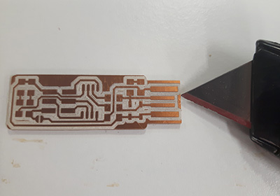
Milling a FR-1 board via Fab Modules. FR-1 consists of a thin layer of copper over a non-conductive phenolic resin. When the external thin copper layer is milled away, what is left are traces to which electronic components can be soldered and connected to each other.
I downloaded Brian’s .png -files Traces (1000 dpi) and Outline Cutout (1000 dpi) below,

and did fabmodules.org to make the .rml -files for Roland SRM-20 milling machine as follows.
The .rml -file for traces:
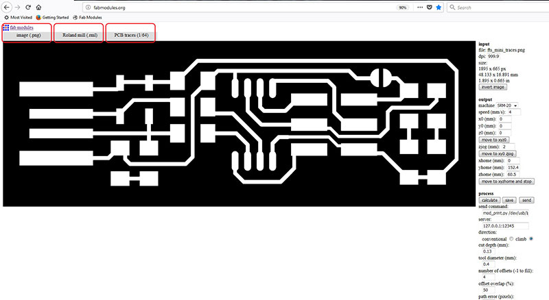
- Navigate to fabmodules.org
- Set input format to be image (.png) and navigate the png image “fts_mini_traces.png”
- Set output format to be Roland mill (.rml)
- Set process to be PCB traces (1/64)
[This time it was simply checking, when the .png files were ready, but later on I need to define the dpi value when exporting pictures from Eagle, and when opening them in fabmodules.org make sure that they match together.]
Then,
- Select the output machine to be ‘SRM-20’
- Change the values of x0, y0 and z0 (mm) to 0, since on our machine we don’t need this offset, since we will define the origin manually.
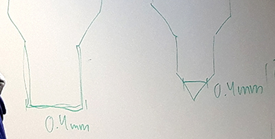
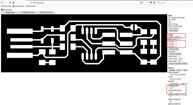
- Define the cut depth (mm) to be 0.10 – 0.14 (mm) telling how deep the cut will go. And, in case of v-shaped milling bit, how wide the cut will be.
- I set the cut depth to be 0.13 mm based on our group experiences in the linetest, where:
- in one hand, at some point, 0.14 seemed to be too much and engraving not only the copper but also slightly a layer below, but
- in another, 0.10 mm seemed to leave too much copper unengraved.
Further, check:
- tool diameter to be 0.4 (mm),
- number of offsets to be 4, for isolation of traces, and
- offset overlap to be 50 (%), meaning each cut overlapping half the previous one. There, the isolation, which is a gap between the traces, has to be wider than the milling cuts.
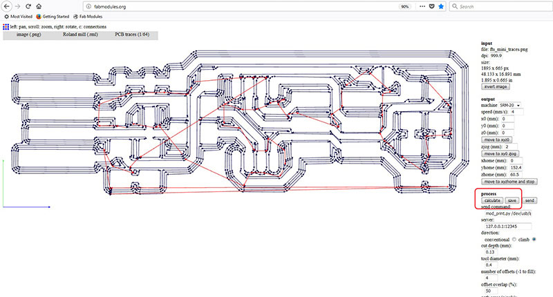
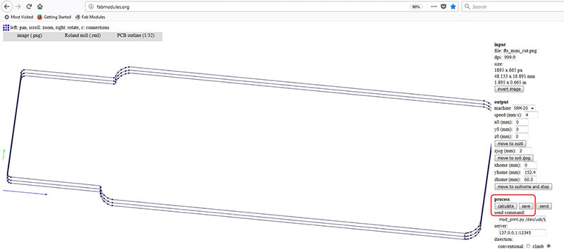
Press calculate to see the blue lines the milling machine will draw (the ‘number of offsets’ - in this case four of them in everywhere), and the red lines telling how the milling bit will move between the cuts.
Furthermore, save the .rml -file.
The .rml -file for outline:
For the 'outline fts_mini_cut.png' -file, follow similar steps in fabmodules.org that you did for traces, but
- Set process’ to be PCB outline (1/32).
Then, check that the image size matches with the size of previous one.
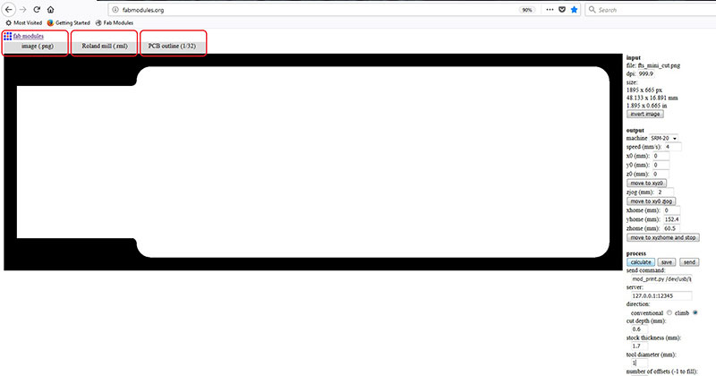
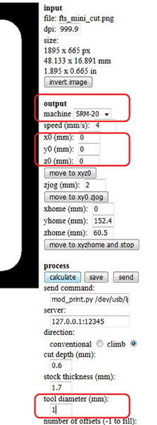
- Again, set output machine to SRM-20 and
- Change the values of x0, y= and xz0 (mm) to 0.
- Check stock thickness (mm) to be 1.7 mm and lastly,
- Define tool diameter to be 1 (mm).
Press calculate, and save the .rml -file.
Later on, when making my own board, the black outline has to be thicker than tool diameter (1 mm).
Start VPanel for SRM-20.
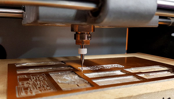
Mill the traces of the board
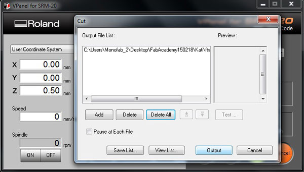
The machine preparation is done so, for milling the traces of the board select Cut.
From the opening window, select Delete All from the Output file list and then, Add new one by navigating the first .rml file of Traces and open it.
When you press Output , everything else has to be done, since it will start cutting straight away.
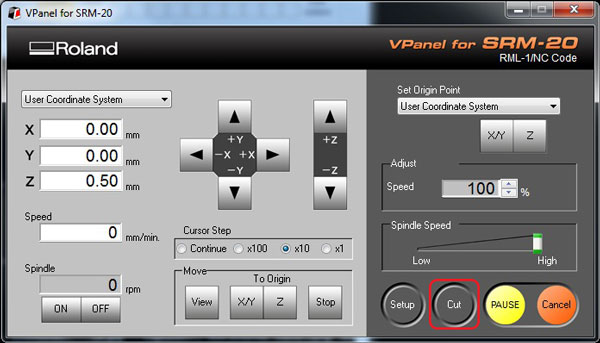
After the first file is cut, without touching the origin, open the door of the machine, cleaned it by a vacuum cleaner and, remove the first milling bit.
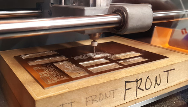
Mill the outline of the board
Change the milling bit to 1 mm bit.
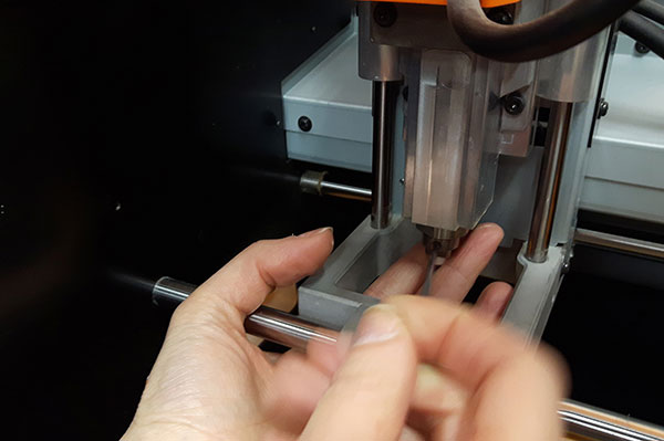
Repeat the steps done for the first .rml file for cutting the outline and being able to remove the cut board from the sheet:
Do not make any changes for X/Y-origin, but find the Z-axis Origin Point:
- Move the Z-head and the milling bit near the surface of the board,
- Loosen the screw in the shank by allen key for letting the bit fall and touch the surface,
- Fasten the screw by holding the bit still so it won't move up when fastening, and
- reset Z-axis.
- Then again, raise Z-axis and the milling bit slightly from the surface and 'Cut'.
In VPanel, select Cut. From the opening window, select Delete All, then Add new one by navigating the second .rml file of Outline and opening it.

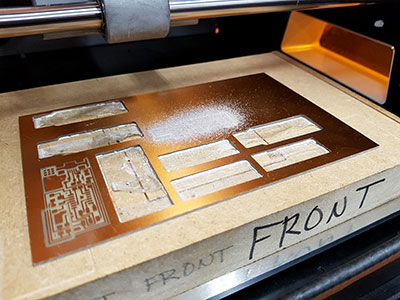
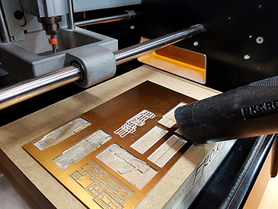
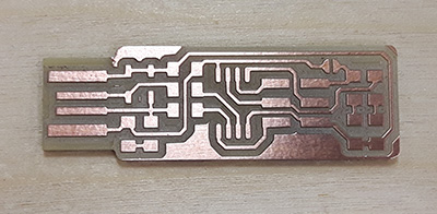
After cutting, clean and remove the cut board carefully, and clean the milled board from dust by rinsing it under the water.
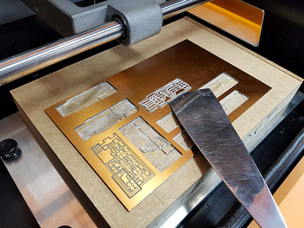
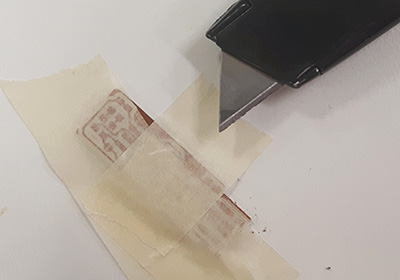
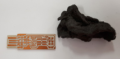
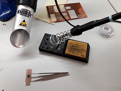
As Brian and our own instructors instructed, I removed some external copper by sharp knife, and the photo sensible layer at the top of the surface of FR-1 by using metal wool. I attached the board to the table by tape which both hold it as well as protected it from the knife if it would have slipped a bit.
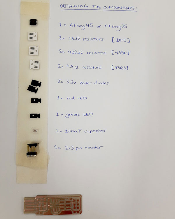
Components
I collected all the necessary components according to Brian's instructions. As a great tip from one of our local instructors Iván Sánchez Milara I labeled the components to a sheet of paper attached by tape, which made easy to recognize the components and see the whole, and pick up the right component during the assembling process.
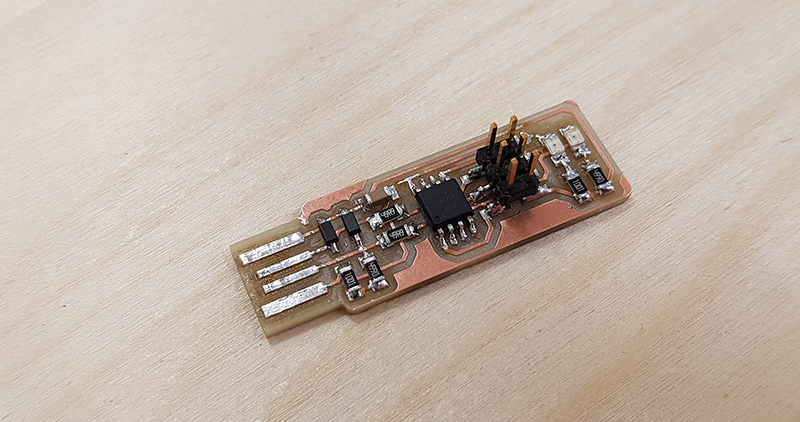
Assembling the PCB
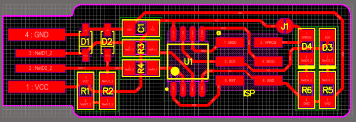
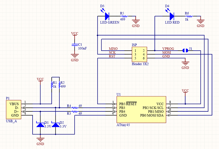
The board layout and schematic images I utilized in assembling process are obtained from Brian's:
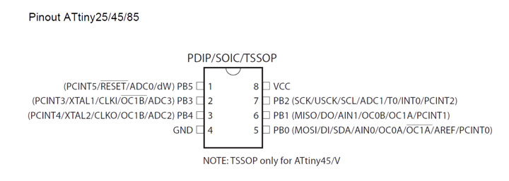
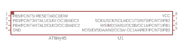
Here is ATtiny45 Pinout obtained from the Datasheet.
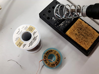
First of all, I collected the tools needed: soldering iron, soldering tin, desolder braid, tweezers, and microscope, and wet the sponge of soldering iron for cleaning the tip of the iron.
Preparing to start soldering, I turned on:
- 1) the main switch and the power of soldering iron, and waited for the temperature of it to be 350 °C.
- 2) the two main swiches for flexible “stayput” arm removing the fumes and gases caused by soldering.
Then, I figured out the order of soldering the components to the board. I have soldered a few times but I am not too experienced in that so, I was excited about the assigment. Jari instructed us follow the rules from:
- the hardest to the easiest
- the lowest to the highest
- the middle to the edges .
So, I ended to do my soldering process in the following order:
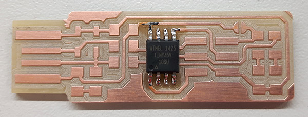
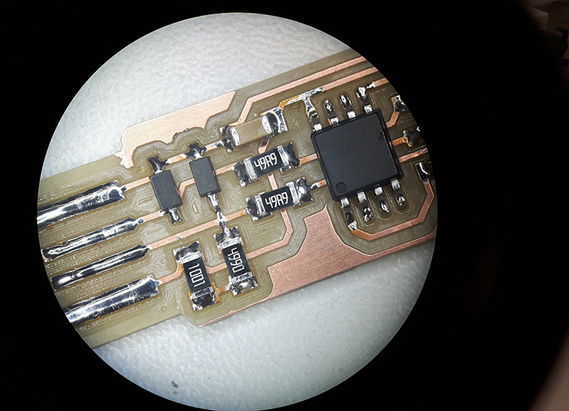
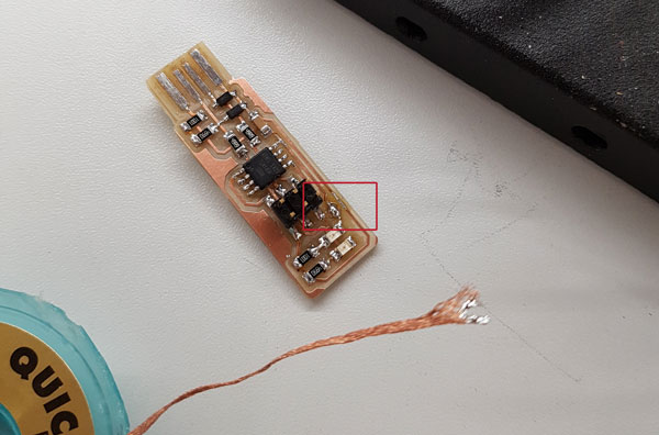
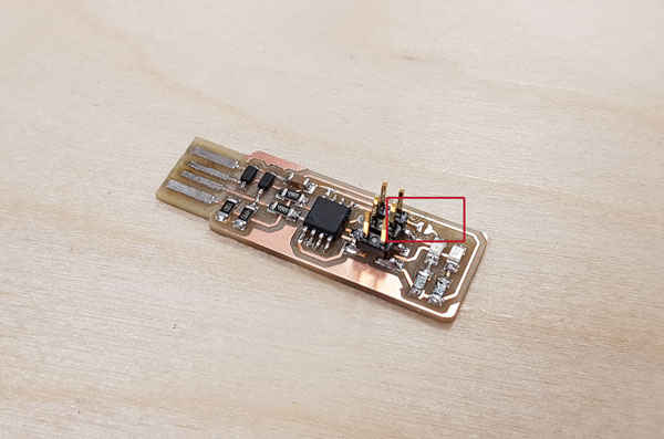
I started from the ATtiny45V microcontroller standing in the middle, being low and having eight small pins. ATtiny45 is a high performance, low-power AVR 8-bit microcontroller based on the AVR enhanced RISC architecture. When placing the microcontroller, check the orientation by the small dot in the left lower corner meaning pin 1 against the schematic and PCB lyout image.
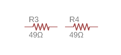
I continued with surface-mount 49Ω resistors [49R9] next to ATtiny. Resistors are electronic components which have a specific, never-changing electrical resistance limiting the flow of electrons through a circuit. At this board, is a passive component consuming the power (without generating it) added to the circuit to complement the active component microcontroller.
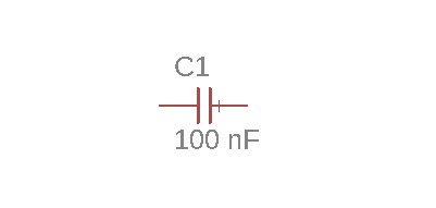
I assembled 100nF capacitor next to resistors. Capacitors are built to have a specific amount of capacitance. The capacitance of a capacitor tells how much charge it can store, where the more capacitance means the more capacity to store charge. The standard unit of capacitance is called the farad (F).
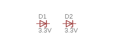
Next to previous ones, I assembled 3.3v zener diodes. Zener Diodes are often used to create a known reference voltage at exactly their Zener voltage. Zener’s are designed to have a low and specified breakdown voltage (or zener voltage) meaning, that when enough current runs in reverse through the zener, the voltage drop across it will hold steady at the breakdown voltage.
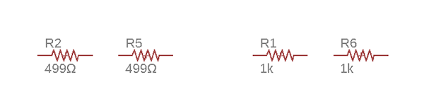
Then, I continued to assemble the surface-mount 499Ω resistors [4990] for avoiding to burn the green LED, and 1kΩ resistors [1001] for avoiding to burd the red LED, following the order from inside to the edges.
When assembling the red LED and green LED, the orientation did matter again. I checked the green line where the side with the line is the cathode connected to the ground and without line is the anode connected to the VCC.

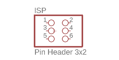
Finally, I added 2x3 Pin header for programming the board.
Be careful to check the orientation of the components:
- ATtiny45 has a dot laser-etched into the lower left corner marking pin 1.
- LEDs have green line to mark the cathode connected to the ground.
For adding a component:
- Use hot soldering iron to heat up the metal pad on the board, and apply a small amount of soldering tin to the pad.
- Use tweezers to place the component in the right position and hold it, solder the first leg by heating the tinned pad untill the leg is fixed.
- Then, in the crossing order, solder rest of the legs and finally, add a little bit more tin for resoldering also the very first leg.
- Make glossy and beautiful joits by heating enough to make the joints wet.
After each piece of soldering:
- Clean the tip of the soldering iron using a wet tip cleaning sponge, in order to facilitate the joints.
- Make sure that all of the components and their legs touch the board's pads so they are flat on the board, not only laying in the air by tilted with pins.
- Check the assembled board against the board schematic and board layout images to make sure that there are correct components placed correctly in correct orientations.
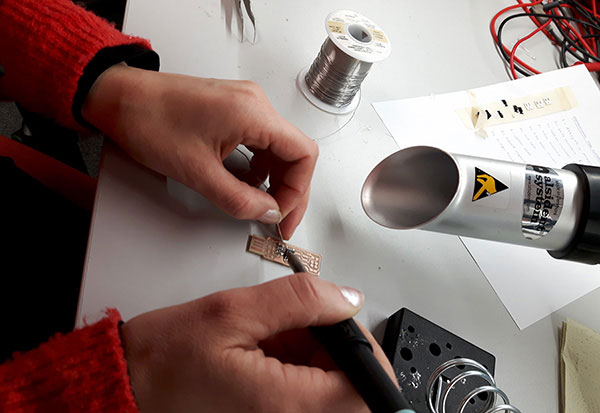
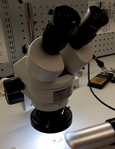
I used a microscope to check my joints every now and then.
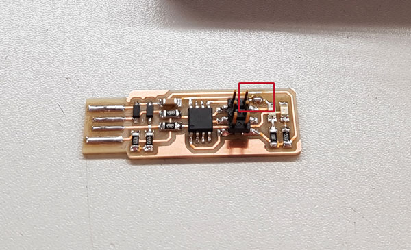
In the end, I soldered a bridge to be a temporary connection between the connector pads near red LED (in the board layout and schematic marked as J1). This way the programmable board supplies voltage on this pin and the programmer board detects it.
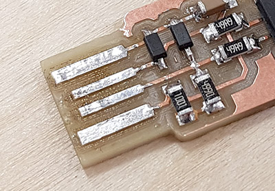
To ensure a good USB connection, I added a little bit soldering tin for the pads. However, in he beginning I didn't realise that there is no need to be huge layer of it but only for the surface. Having too much could actually even weaken the connection so, I reduced the amount of tin by heating it together with desoldering braid, and then leveling the surface.
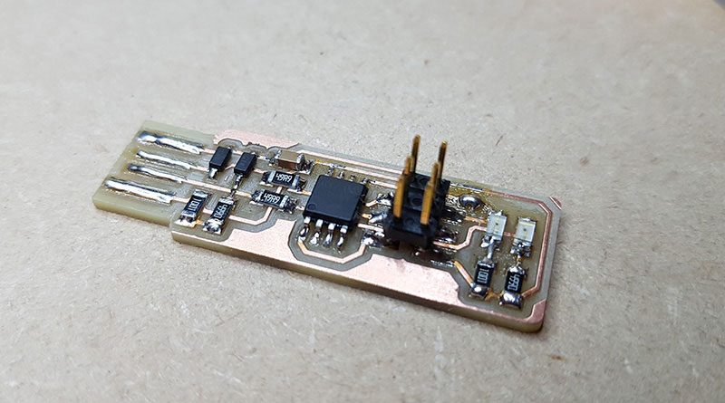
Assembling finished.
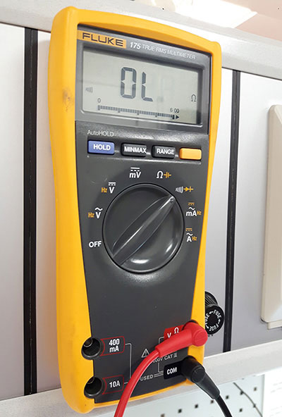
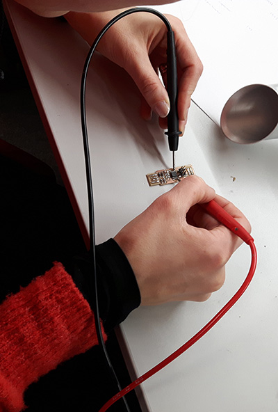
When finishing the assembling, I tested my board by multimeter to be sure that all the connections function (shorts between Vcc and GND) and there are no short circuits.
Programming the PCB by FabISP programmer
After finishing assemling and testing, before I was able to build and program the firmware onto my board, I had to set up my development environment. To do that, I followed Brian's great instructors for Software Installation for Windows and Using the GNU AVR toolchain on Windows 10.
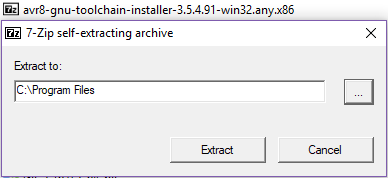
1) First of all, Install the Atmel AVR Toolchain for Windows from Atmel's site and ran the installer. Pay attention to extract the files to C:\Program Files.
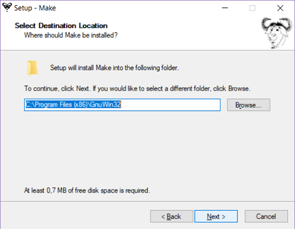
2) Next, download Gnu Make and launch the installer. Accept the default location for the installation, which seemed to be C:\Program Files (x86)\GnuWin32.
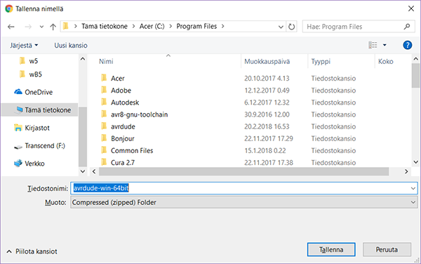
3) Download avrdude, unzipp the folder and copy the archive 'avrude' inside of it to C:\Program Files.
For finishing these tool installations, modify the Paths in order to tell Windows the locations of the tools.
- Open the Start Menu > Control Panel.
- Since there was no "Advanced System Settings" visible, I used search function to navigate my way to Environment Variables.
- From the opening window I selected Path and Edit.
- In case you don't have a variable called Path, check Brian's instructions to create it.
As Brian advices, I added following three lines into the list:
- C:\Program Files\avr8-gnu-toolchain\bin
- C:\Program Files (x86)\GnuWin32\bin
- C:\Program Files\avrdude
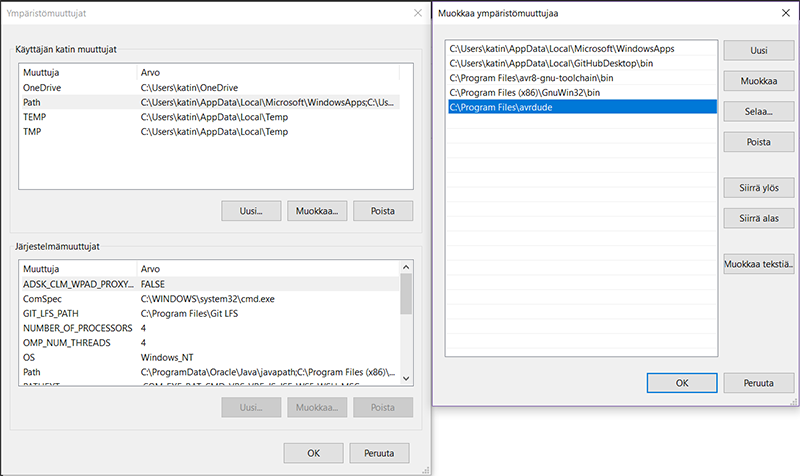
and confirmed the modifications by clicking OK for each of the windows opened.
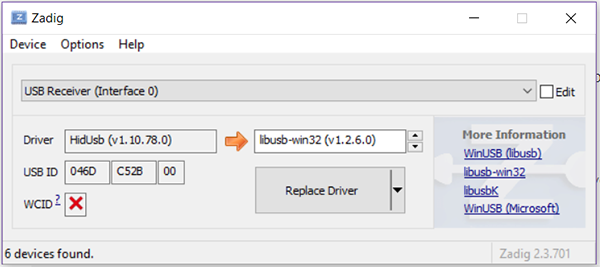
4) Next step and as a last part of the installations, was to install drivers for my programmer. For Windows users, Brian advices us to use a helpful tool Zadig.
- I plugged in the already programmed programmer, which I borrowed from our local instructor Antti Mäntyniemi, and
- selected the "USBtinySPI" device in the list.
Then, I installed the driver libusb-win32.
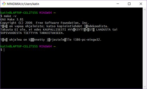
In order to check that everything are in the right folders and installations are finished succesfully, I opened Git Bash.
In Git Bash, I got expected result by typing:
make -v
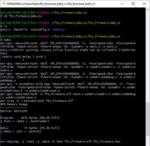
Then, I continued building the firmware.
I downloaded the firmware source code and extracted the zip file. In Git Bash, I navigated into the source code directory [C:\...\fts_firmware_bdm_v1\fts_firmware_bdm_v1], and ran make. The command built the fts_firmware.hex -file, that I was going to program onto my ATtiny45.
make
Since the Makefile assumes that the programmer belongs to the usbtiny family by default, I just checked that it was defined in the file with Notepad++:
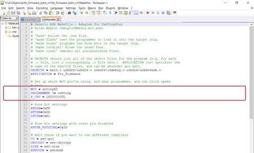
Now, I plugged my board into a USB port by using extension cable, as both Neil and our instructors suggested in order to avoid damaging computer's built-in USB ports by soldering tin, and got the red LED light up.
Next, I connected Antti's programmer to the ISP header on my board checking carefully the orientation of the cable so, that pin1 (marked with small dot in the board diagram and in the ATtiny45 microcontroller) was connected to pin1.
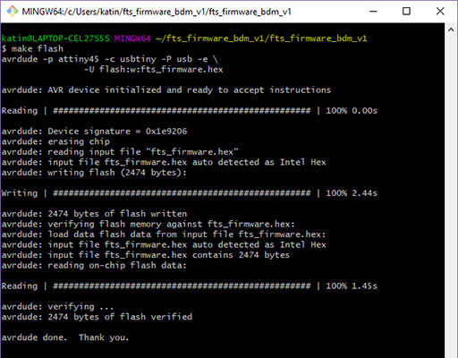
Then I ran make, which erased the target chip, and programmed its flash memory with the contents of the fts_firmware.hex -file. From the processes below can be seen how avrdude erased (erasing chip), programmed (writing flash), and verified (verifying flash memory against fts_firmware.hex) the chip.
make flash
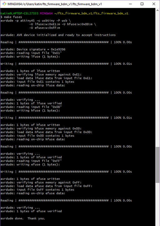
After programming the flash memory, I set the configuration fuses. The fuses control where the microcontroller gets its clock source from.
[Also, after making sure that the board has succesfully programmed to be a programmer, the fuse disabling the reset pin and turning it into a regular GPIO in will be set. This allows the chip use the reset pin for programming other boards, but will disable the ability for this chip to be reprogrammed.]
For setting up all the other fuses except the one mentioned above, I ran the command:
make fuses
Then, I navigated myself to Device Management to check if my board would be visible in there, and it was under the USB devices.
Now, the ATtiny45 on my board has the code loaded onto it, and my FabTinyISP microcontroller is programmed. The original program memory is re-programmed, and the new program is stored in non-volatile memory meaning that ATtiny45V will remember the program.
Finally, next two finishing steps turned my board into a programmer that can be used to program other boards.
First, I turned the ATtiny45's reset pin into a GPIO pin by finishing the fuses using make rstdisbl command, which does the same as the 'make fuses' did before, but adds that final command disabling the ability to reprogram this chip anymore.
make rstdisbl
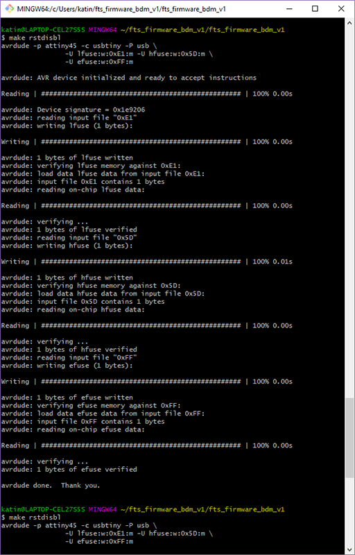
Second, in order to turn my board from the programmable board into the programmer board, I disconnected Vcc from the Vprog pin on the ISP header by removing the temporarily bridge (breaking the connection between the connector pads near the red LED - in the board layout and schematic marked as J1) by heating the solder pad through desoldering braid with soldering iron.
To test complitely whether my programmer works, we used it to program my fellow student Jari's board. Many thanks for Jari for his support on this programming process.
When writing the documentation I finally understod better what happened during the programming process.
I need to make a nice holder for my programmer in order to make it fit with USB-port.
Here are the .rml files of The FabTinyISP I reproduced this week.