Week 6 Electronics Design
-
Use an EDA tool to design a development board that uses parts from the inventory to interact and communicate with an embedded microcontroller
-
Group Project: Use the test equipment in your lab to observe the operation of a microcontroller circuit board (as a minimum, you should demonstrate the use of a logic analyzer)
-
Group Project: Document your work on the group work page and reflect what you learned on your individual page
Link to group site
Board Design
This week I wanted to use an entirely new input. During week 4 (Embedded Programming) I used buttons for everything and now I want to try something new. I decided to use a LDR photoresistor. I decided to use an LED as an output. Basically my board idea is a flashlight that automatically turns on.
I decided to use a voltage divider for the LED. A voltage divider would allow the the microcontroller to be able to detect changes in voltage from the LDR. Then, I can send that voltage into the microcontroller via a ADR pin. Since the LDR is a conductor when there is light and a insulator when there isn't light, I would have a simple code stating if the voltage is lower than a certain value, turn the LED on, and when the voltage is higher, turn the LED off.
How do LDR Photoresistors work?
LDRs are a semi conductor material (Cadmium Sulfide). When Photons collide with the Cadmium sulfide, the energy knocks electrons from the valence band to the conductive band. As more electrons are transerred from the valence band to the conductive band, more current is able to flow through the LDR.
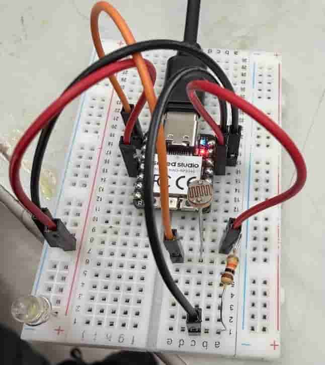
I designed this breadboard with a Xiao RP2040 microcontroller. I used a voltage divider with the LDR as one of the resistors. I added a wire going from in the middle of both resistors acting as a tap. That wire goes to the ADC pin on the micrcontroller. The microcontroller reads it as an analog input and not digital because the voltage varies and doesnt act like 1s and 0s.
Code
I consulted copilot for my code. I told it:
"I am a Fab Academy Student. I am trying to design circuit where an LDR communicates with a Xiao RP2040 micrcontroller and then turns an LED on depending on the voltage from a LDR. I am using a voltage divider with the LDR as one of the resistors. I have a wire going from in between both resistors to ADC0 on the microcontroller. The microcontroller should read the voltage coming from the LDR as an analog value. When the voltage drops below a certain value, turn the LED on and when the voltage goes above that value, turn the LED off. The LED is connected to micropython pin P29. Can you generate code that fits these requirements?
Copilot responded with this code:
from machine import Pin, ADC
import time

ldr = ADC(26)          # D0 = GP26 = ADC0
led = Pin(29, Pin.OUT) # D3 = GP29

THRESHOLD = 30000      # adjust after testing

while True:
    value = ldr.read_u16()
    print(value)

    if value < THRESHOLD:   # DARK → LED ON
        led.value(1)
    else:                   # BRIGHT → LED OFF
        led.value(0)

    time.sleep(0.1)
I uploaded this code to the Xiao RP2040 via VSCode and then the code worked first try!
I took the circuit into a small room with a light switch so I could test my circuit. As you can see it works!
EDA Tool: KiCad
Kicad does not include a Xiao RP2040, luckily Kicad has a plugin menu. I downloaded and installed the FabLib Library. This included the Xiao RP2040 and many other electronics used in fab labs.
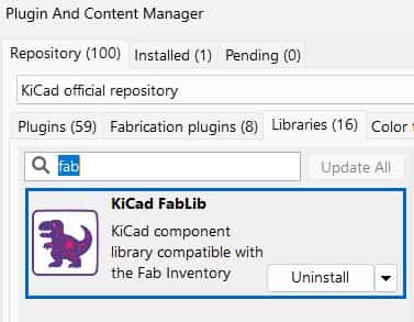
Here is the plugin I installed. In Kicad I went to Plugin and Content Manager -> Libraries then searched FabLib.
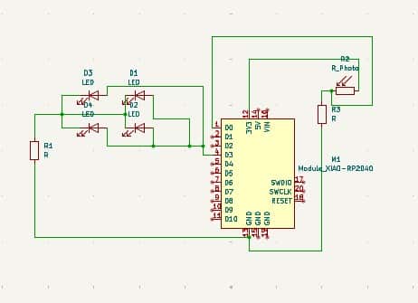
I designed this in the schematic editor. I connected all the connections that needed to be together so later in the pcb editor I could know what to connect. I also added 4 LEDs instead of one because I wanted a brighter light.
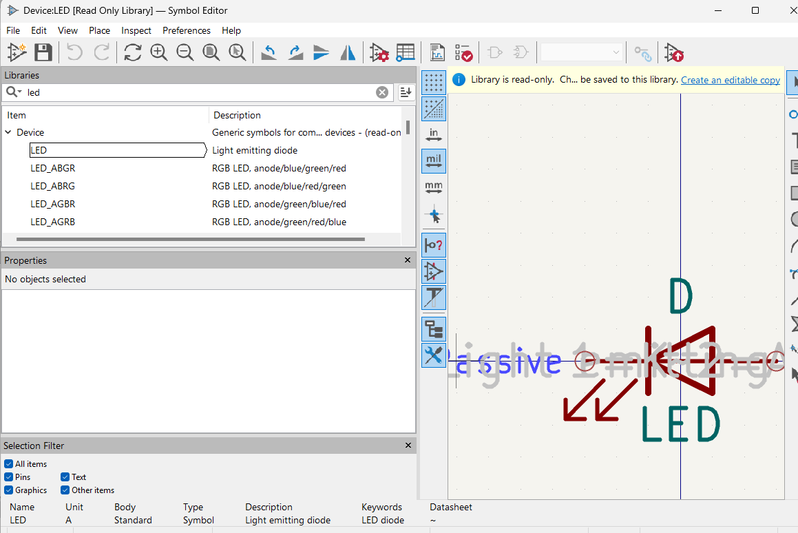
To add a component, I went to the symbol library above. Search any component, I searched for an LED. Then click on your component.
Once you pull up the component, press the upload button on the far right. This will add the component to your schematic.

Once the component is in your schematic, to connect it to other components, you need to draw wires.
On the menu on the right, select the wiring tool that is selected in the image. Once selected, just click and drag the wires to connect components. It is super easy to use.
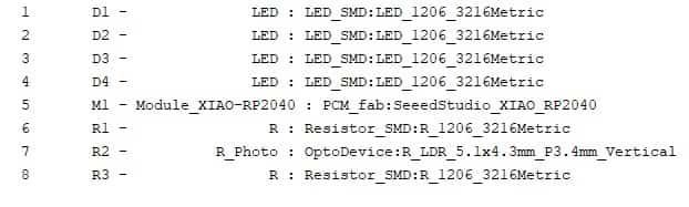
Here are all the footprints I assigned. I chose to use surface mount LEDs and Resistors. Out lab uses size 1206 so I made sure to select those ones. I measured the size of the LDR and chose the correct sized footprint. The RP2040 came with its own footprint.
ERC
The ERC is located in the top menu of the schematic section
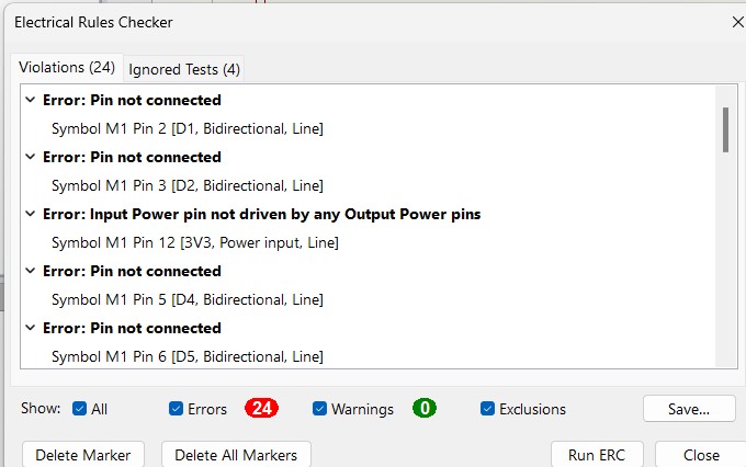
Here, I ran the ERC (Electronic Rules Check). The ERC makes sure your schematic follows electrical rules. If you accidently connect a positive to a positive, or make some other electronic mistake, the ERC will let you know.
In my ERC, I have many errors, however all of these can be ignored. When using a Xiao component in Kicad, and not all of the pins are connected to something, the ERC will detect that as an error. Since I did not need to use all of the pins, these error messages can be ignored.
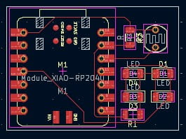
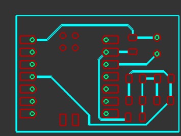
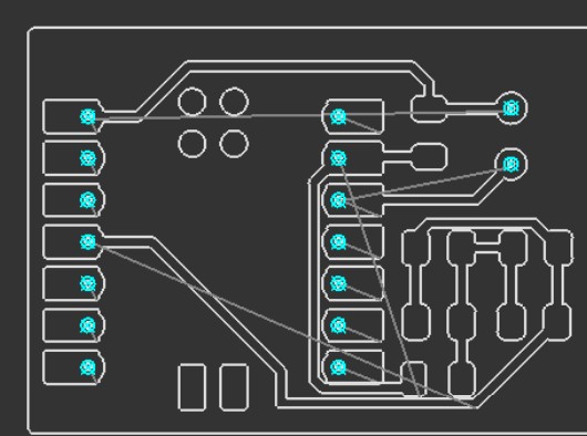
I designed this PCB in the PCB editor section of Kicad. After I finished everything in the schematic editor, I switched and updated the PCB editor. I arranged all of the components then drew the traces. I made sure to do all of the traces on F.CU which is the front of the copper. After all the traces were drawn, I switched to Edge.Cuts to draw an outline for the board. For this board, a small rectangle was sufficient.
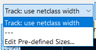
Here is where you can change the width of the traces. For this board, I used the netclass trace width set by KiCad. If you wanted to change the trace size, click the three dashes, then set your trace width in mm.
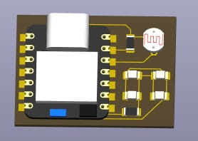
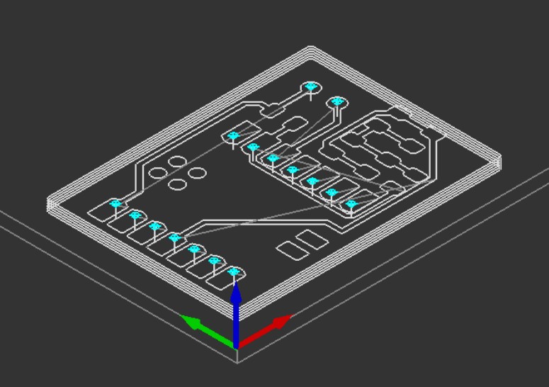
After finishing the pcb, I clicked the 3D viewer to see my pcb. This is the complete pcb. Some of the traces aren't visible, they are under the microcontroller, however they don't touch any of the pins or pads so it is completely safe.
Ability to be fabricated
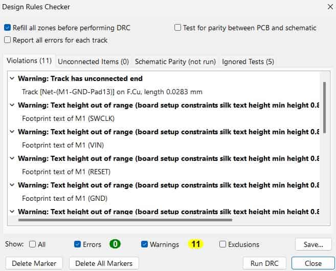
After completing my board in the pcb editor I ran the DRC. This feature checked if my board is able to be created. After running the DRC, I only got a few errors, none of which are important or affect the ability of my board being able to be created.
*Exporting For Fabrication
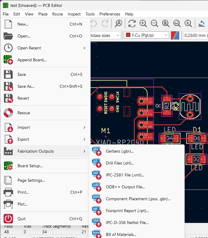
Here you can see how to export the design for fabrication. For this board, I would save the traces and edge cuts as gerber files, then save the through holes for the LDR as drill files.
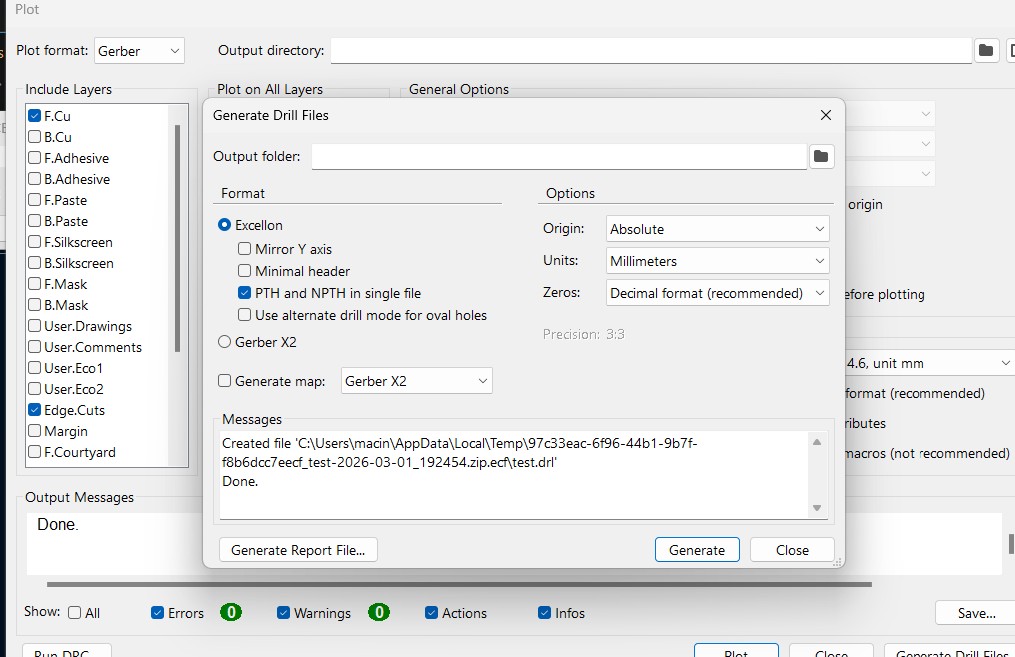
Here, you can see the windows for plotting gerbers and generating drill files. For the gerbers, I only selected the edge cuts and the front copper. for the drill files, I generated drill holes for all the through holes in the project.
Click Here to Download the gerbers and drill files
I imported the gerbers and drill files into makera. The point of this was to test if my design could be made.
Above, I generated toolpaths to test if my design was able to be made. I encountered no errors during this process, and my toolpaths to not intersect or anything bad.
(The grey lines map the path that the tool moves above my board).
MODS
This week, I also used MODS to test if my design is able to be milled. Milling, the main method used to make PCBs in fab labs, is a subtractive manufacturing method. With subtractive manufacturing, you can often run into design issues. MODS is a way to test if you run into any of those design issues.
To use MODS, first convert traces to an SVG or PNG file. Make the traces white, and the background black. Once the SVG or PNG is made, import it into MODS. Select tool size (For example 1/64, 1/32, 0.3mm, etc. Whatever milling bit you will use). Selecting the proper tool size ensures that MODS accurately represents the milling process. When MODS generates the test, look for excessively thin traces, are there toolpath overlaps, do any islands form, do all paths reach where they need to be, etc. MODS helps answer these questions that the standard DRC in KiCad does not answer.
When my board looked accurate in MODS, I knew that my board could be made using subtractive manufacturing. MODS let me know that I did not need to make any adjustments in the PCB editor in KiCAD.
Reflection
I found the individual portion of this week to be very easy. All I had to do was design a simple board and then use an EDA tool. I had already used Kicad and it is my labs main EDA tool so the board design process felt easy. The group work felt harder this week. Me and my group were tasked with using tools in our lab to analyze electronics. Tools like the Osciliscope and especially the Logic Analyzer were new and took a while to learn. The Logic Analyzer was especially difficult because there were around 30 wires sticking out of it that I had to figure out.