08. Electronics Production
view Checklists
*Checklist: personal*- [x] DeepL check spelling, grammar
- [ ] GPTcheck for better markdown
- [x] repair file links, replace .png -> .jpg; .mov -> .mp4
*Checklist: Nueval: General*
Group Assignment - [x] Characterize the design rules for your in-house PCB production process: document feeds, speeds, plunge rate, depth of cut (traces and outline) and tooling
- [ ] Document the workflow for sending a PCB to a boardhouse
- [x] Document your work to the group work page and reflect on your individual page what you learned
- Individual Assignment - [x] Make and test a microcontroller development board that you designed
*Checklist: Nueval: Students checklist*
- [x] Linked to the group assignment page
- [x] Documented how you made the toolpath
- [x] Documented how you made (milled, stuffed, soldered) the board
- [ ] Documented that your board is functional
- [x] Explained any problems and how you fixed them
- [x] Uploaded your source code
- [x] Included a ‘hero shot’ of your board
Group Assignment
The group assignment can be found here
Learnings form the Group Assignment
Mill Bits:
- mill for outline: 0.8 mm flat end mill
- mill for traces/clearance: 0.2 mm V-Bit (60° angle)
Traces:
- min. trace width: 0.01" (0.254 mm)
- typ. trace width: 0.4 mm
Clearance between Traces:
- min. clearance between traces: 0.007" (0.1778 mm)
- typ. clearance between traces: 0.2 mm
Computer Aided Manufacturing (CAM) for PCBs
A CAM is a piece of software, that helps the user to generate tool paths for a certain machine. In this case the CAM turns the traces and pads form the PCB design into .nc code. The .nc code describes which tool, speeds and positions are the targeted.
CAM software is usually not part of a simple CAD environment, sometimes it is included e.g. in Autodesk Fusion360.
MOODS project - Browser CAM
KiCad Layout to PNG file (KiCAD, Inkscape)
Since the MODS project does not support gerber (.grb) as an import option it is always needed to create .png files with the right parameters for the correct operation.
-
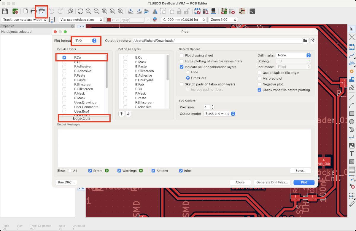
Open KiCad. In the PCB Editor go to 'File' -> 'Plot...' or press the plotter button. Select the svg format and select the desired layers, in this case 'EdgeCut' and 'F.Cu'.
-
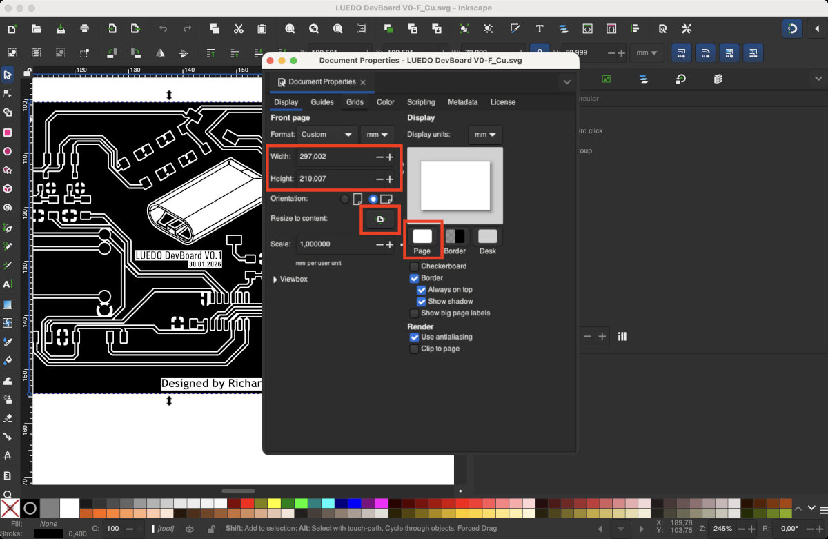
After exporting the layout as .svg, open both files (F.Cu and Edge.Cuts) in Inkscape. Go to 'File' -> 'Document Properties' and:
- Press the 'Resize to content' button
- Add 2mm in height and 2mm in width to the document size
- Change background color to white
-
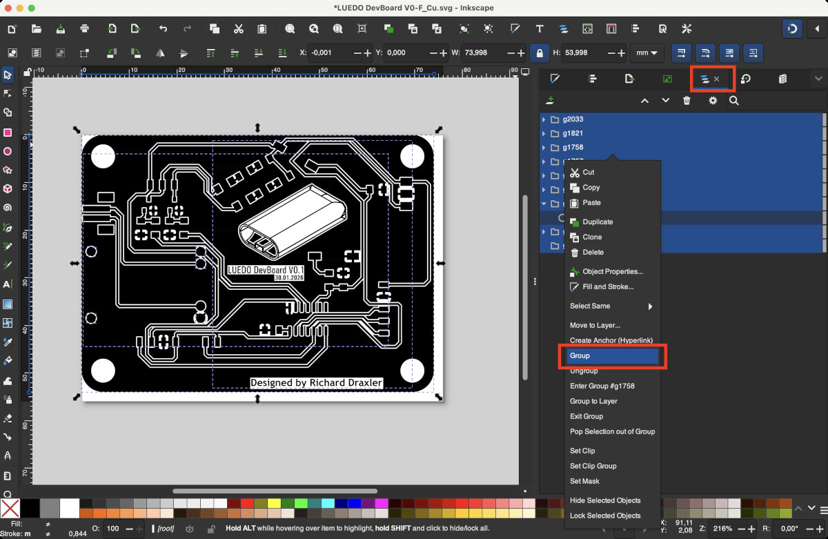
Group all objects to prevent misalignment for the following step!
-
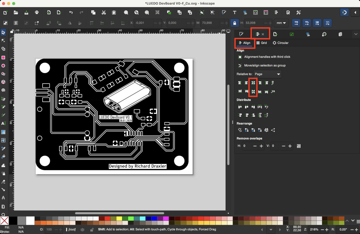
Then align the layout to the center of the page.
-
Go to 'File' -> 'Export'
- Format .png
- Page Tab
- DPI to 1000
- Match Edgecut and Traces in width and hight (pixel dimensions)
- set the background color to white (NOT transparent, otherwise Mods cant detect edges)
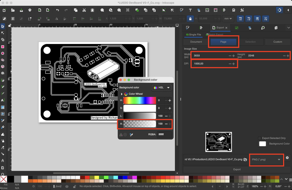
Note
For the edge cut it is necessary to have a black outer border of 1 mm or more. Otherwise, it will not be detected. I created this outer boarder with a paint bucket fill of my existing edge cut (filled with white paint bucket). Afterwords I created a new layer with a black rectangle which is located beneath the other layers.
Note
Make sure the traces image and edge cut image have exactly the same dimensions. The positioning of traces and edge should match in each image relative to the outer perimeter of the image.
Note
While exporting: set the background color to white and not transparent, otherwise the Mods tool will not recognize the traces.
PNG to NC code (Modsproject)
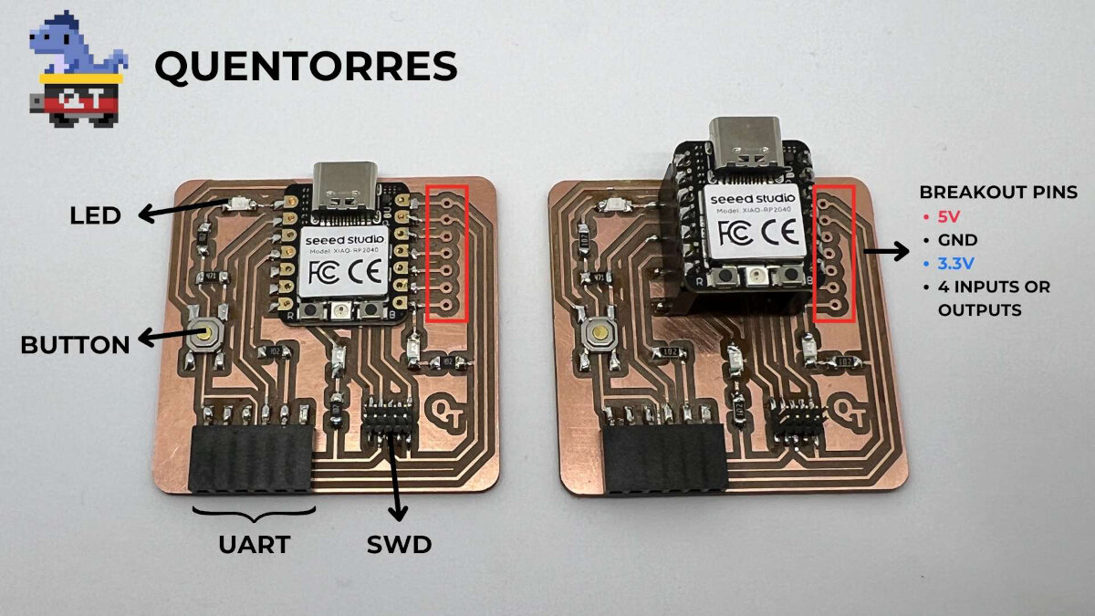
This part of the documentation was written for the Quentorres programmer. I chose this programmer as a starter project since the image files were already provided
Generate .nc code for Traces and Exterior
Go to modsproject.org
- right click
- programs
- open program
- Cavera mill 2D PCB (use the Cavera mill 2D PCB all option if you want to remove all unused copper)
The Cavera mill 2D PCB program is made of different stages/tiles which process the input image and produces the .nc code for milling machines.
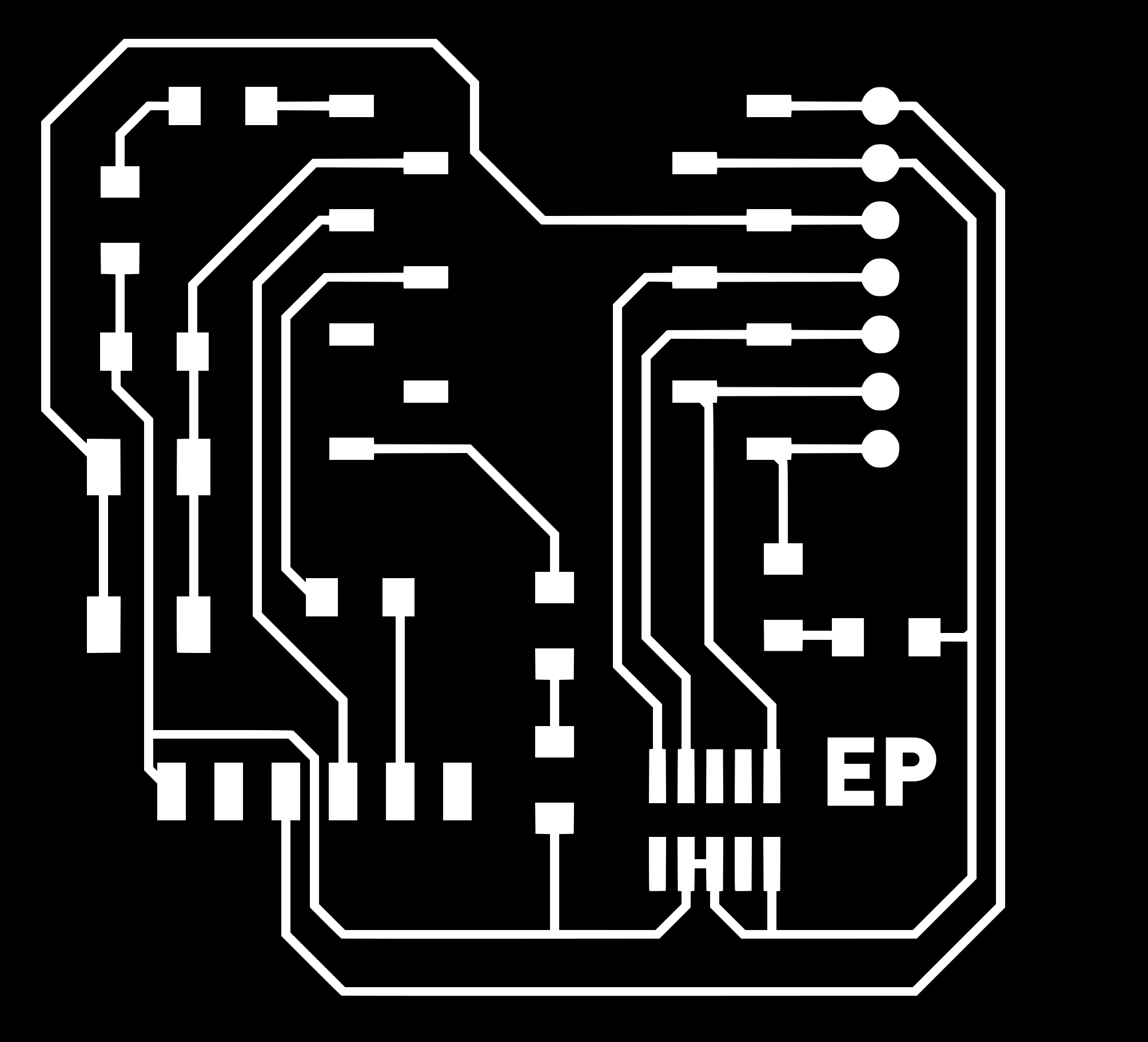
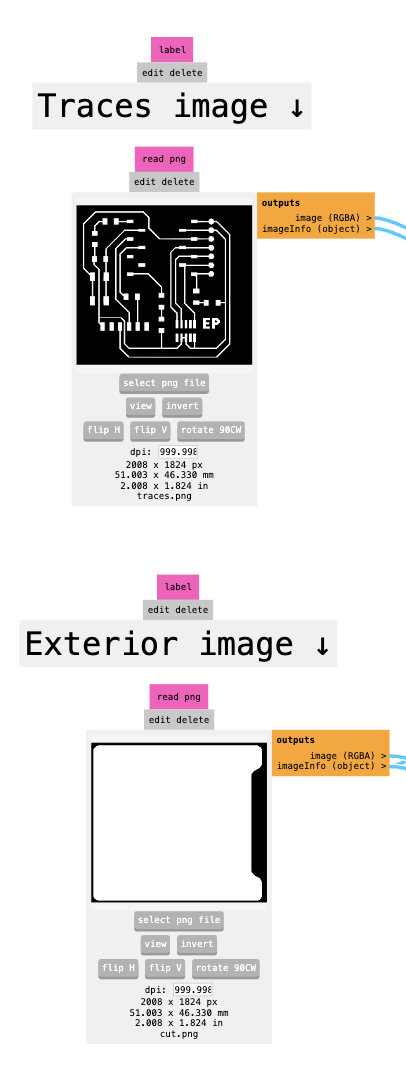
Load the traces.png into 'Traces image' stage and the cut.png into 'Exterior image' stage.
- export your design as png
- traces should be white!
- edge cut should be black! white inside
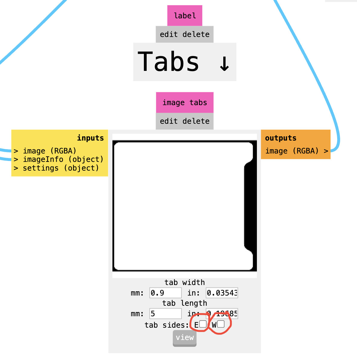
If the PCB is mounted with clamps use tabs to prevent the PCB from moving while being processed.
If the PCB stock is mounted with double sided tape disable the E and W in the tabs stage.
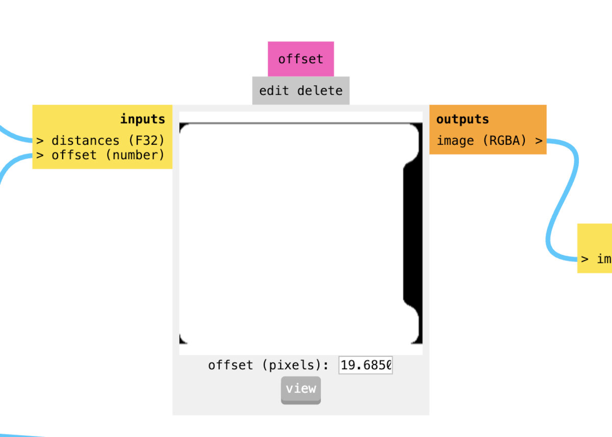
Edit the calculate stage and enter our labs presets.
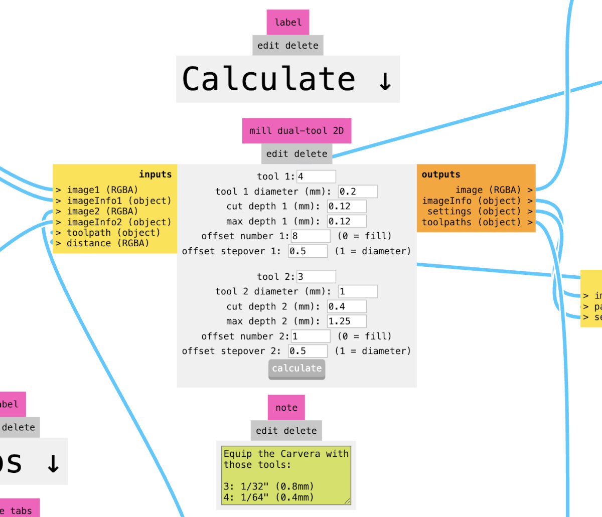
Our labs presets for the Carvera Makera for milling 1.6 mm PCBs.
Tool1: (VCarve bit) (for traces)
- offset parameter defines how much material will be removed
- offset: 0.4 mm bit → 4 (the trace will be surrounded four times)
- offset: 0.2 mm bit → 8 (the trace will be surrounded eight times)
Tool2: (End mill 1 mm) (for exterior cut)
- cut depth: 0.5 mm!
- max depth 0.1 mm less than stock thickness
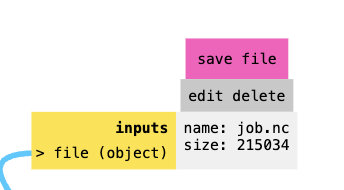
Press the Calculate button and Mods starts to calculate the .nc code. After the calculation is finished the .nc file will automatically downloaded otherwise the job.nc can be manually loaded.
To preview the .nc code go to the view stage.
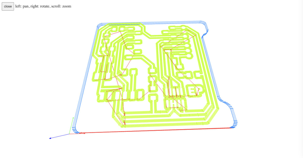
Instead of the internal viewer an external tool can be used e.g. NC Viewer
File:
Quentorres_with_holes.nc
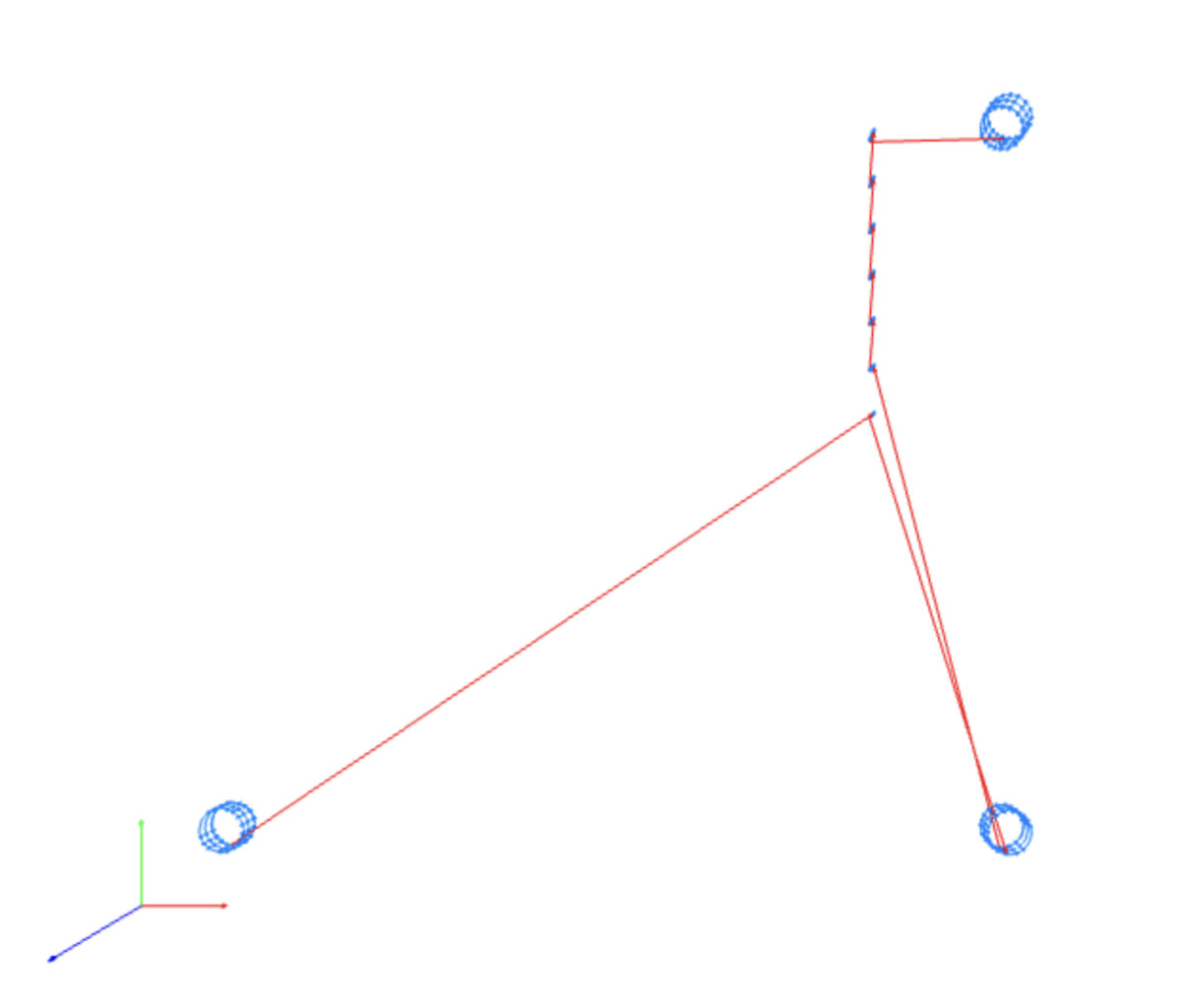
Generate .nc Code for Drill Pattern
To generate .nc for holes I opened an empty mods project and uploaded the 'drill.png' to the 'Exterior' stage. Then I selected in tool 2 a tool which was below or equal to the minimal hole size.
After processing I got this .nc code.
File:
Quentorres_with_holes_drill.nc
Makera CAM (Desktop CAM by Makera)
PCB production on a CNC Mill
PCB stock for milling
Choose PCB material
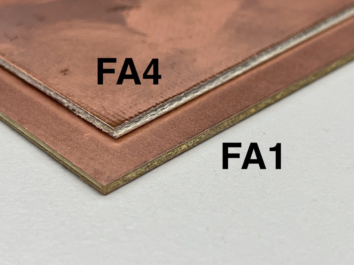
- FR4 is a glass fiber reinforced material
- DON'T USE THIS MATERIAL!
- Glass fibers turn into small particles during milling
- dust is hazardous
- FR1 is not reinforced
- use this material for milling
- double-sided FR1 is available
- alignment and flipping the PCB after the first mill is needed
- not tested yet
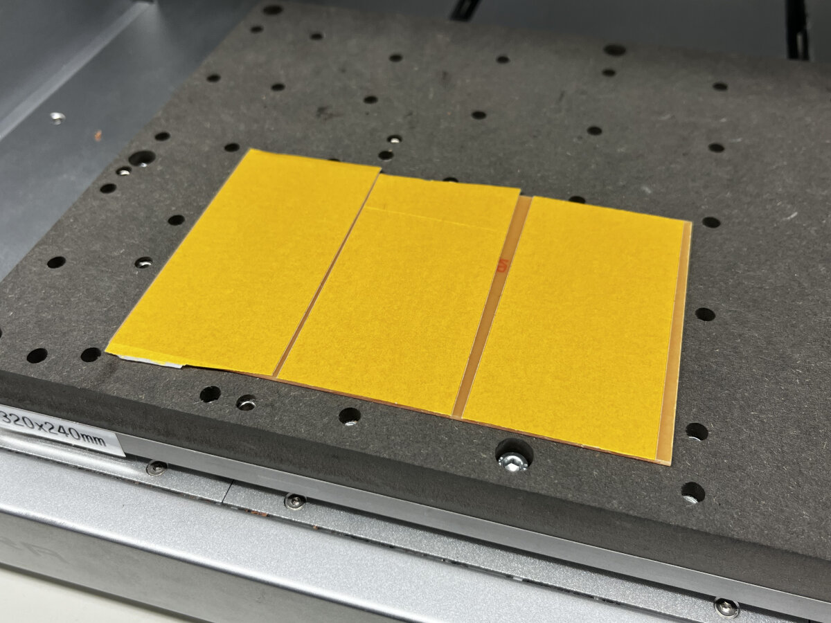
Prepare the PCB for milling
For milling the PCB stock needs to be flat. When the PCB is bend, it will result in uncut traces or to wide/deep traces. To prevent issues flatten the stock first by:
- align with the flat side of calipers, check for light bleed
- correct bends in the PCB
- check again
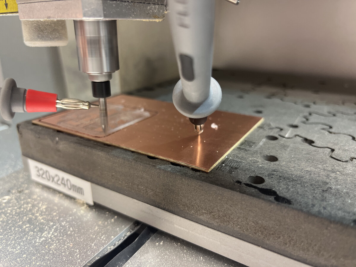
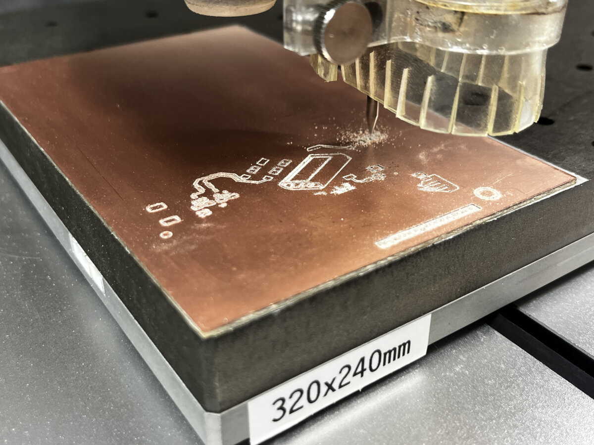
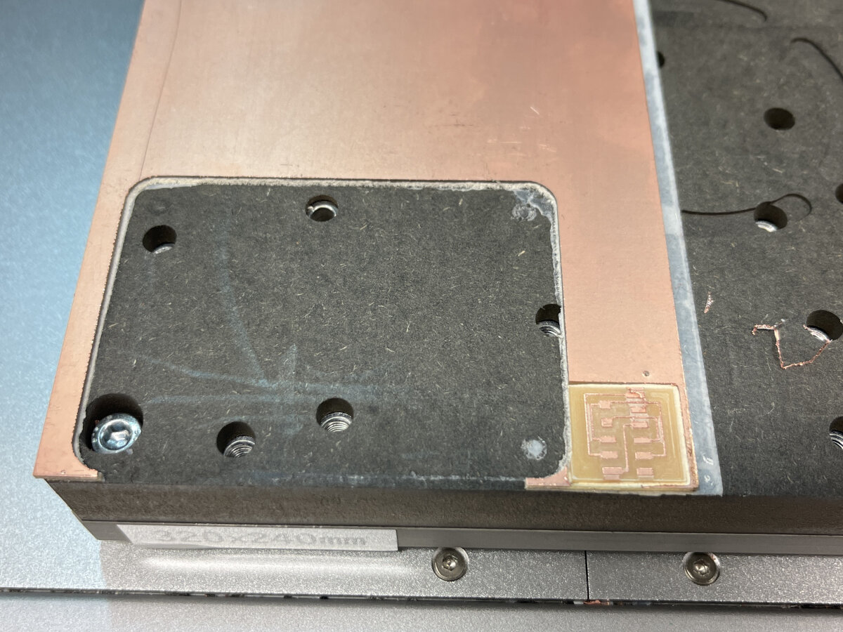
Milling the PCB on the Carvera
- cavera controller
- arrow button → go to the control panel
- work origin is the saved point by the user
- do not use the A button (is used for 4th axis)
- position your head on your new origin position
- right click on x, y, z reset to zero
- pickup tool
- usually we would use the wireless probe (if available)
- manual positioning
- probe the material with the milling head!
- open G-Code command window with
MDI button - M3 to start the spindle (capital case M!)
- use multimeter and lower until contact with the surface of the PCB
- press "stop" in the bottom right corner to stop the spindle (pressing M3 does not work again)
- stop spindle to set origin position
- set z to zero
- open G-Code command window with
- probe the material with the milling head!
- upload a file to the internal memory of the Carvera
- settings button
- disable scan margin
- disable auto z probe
- check position of the origin
- place hand on red Stop button!
- press
Runto start the milling process
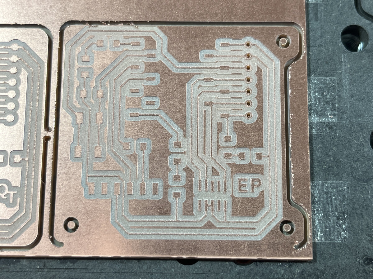
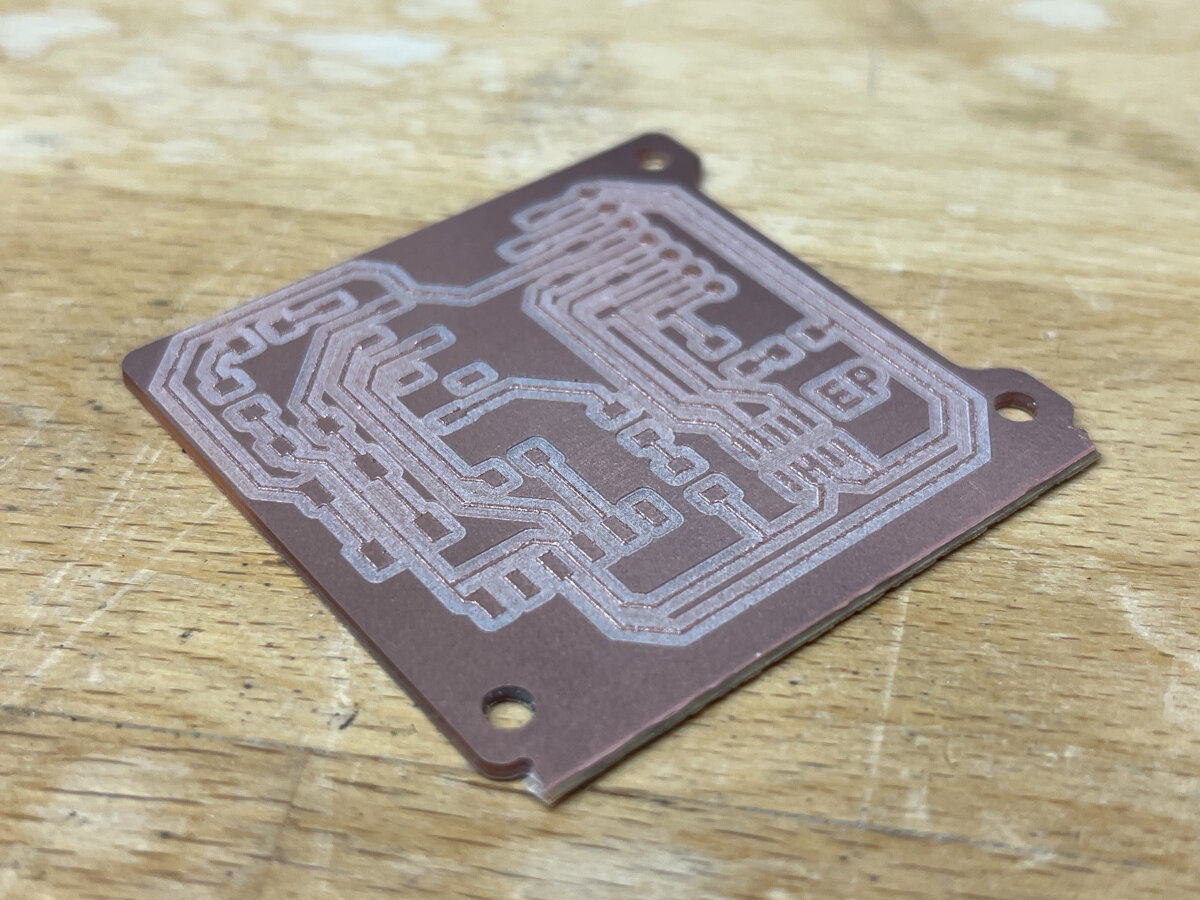
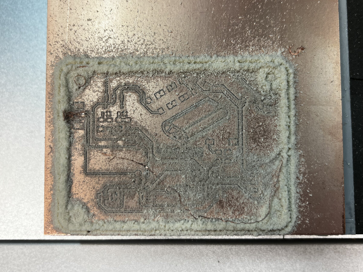
This is the final result after running the traces and exterior cut and the additional drill code.
Issues
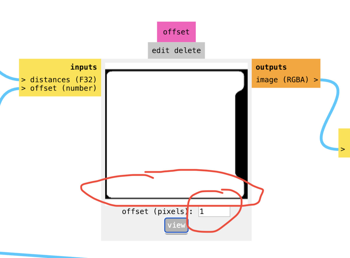
Edge cut is not fully executed
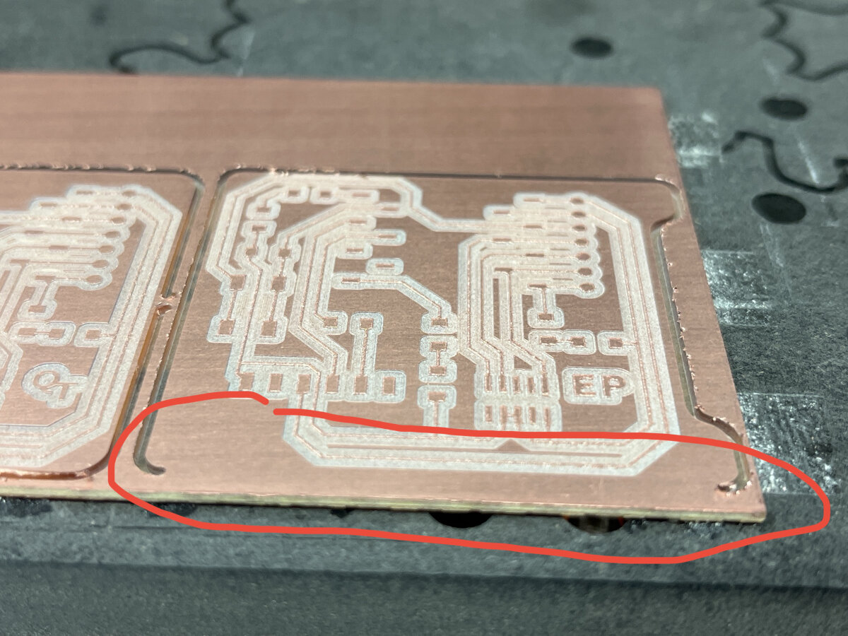
The front contour of the PCB was not fully cut.
During the Mods processing there is a step called 'offset' which cuts the outer contour of the image. This created an issue with generating the .nc code which resulted in an uncut side of the PCB.
Fix the issue:
When the offset is reduced, the contour is turned into a path. Make sure the edges of the edge cut are at least 1 mm away from the outer perimeter of the image.
Postprocessing the PCB
After the milling process there are still a ridge of copper on the surface. To remove the ridge, steel wool is used.
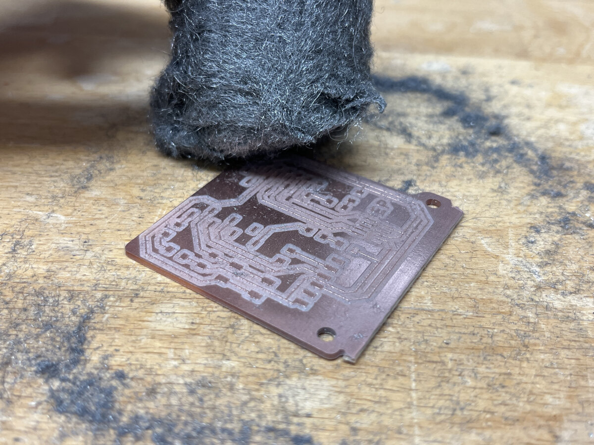
Use steel wool to remove the ridges on the surface. Scrub continuously in the same direction to obtain an even texture.
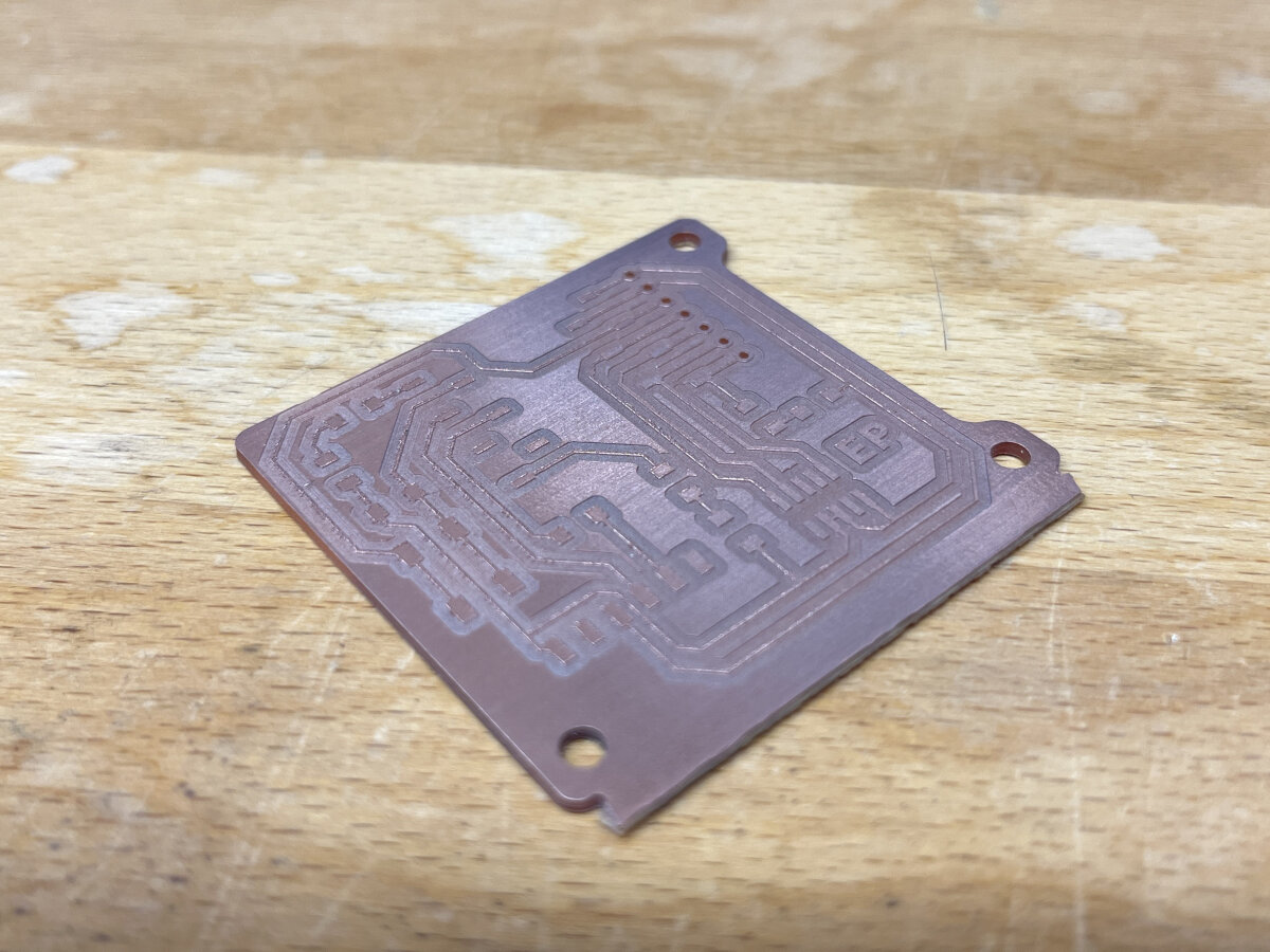
PCB after removing the ridges on the traces.
Once the milling result is visually verified, clean the PCB with water and dish soap, removing any oil and milling residue to prepare the board for stuffing.
SMD Soldering
Since I am quite familiar with soldering (and SMD soldering), I kept this part of the documentation short.
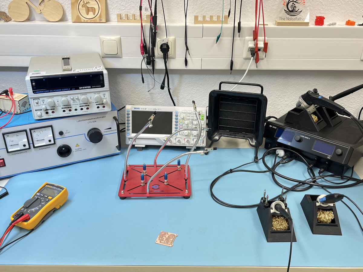
Soldering setup in our lab: Lab bench power supplies, oscilloscope, fume filter, soldering station with: iron, hot air and tweezers
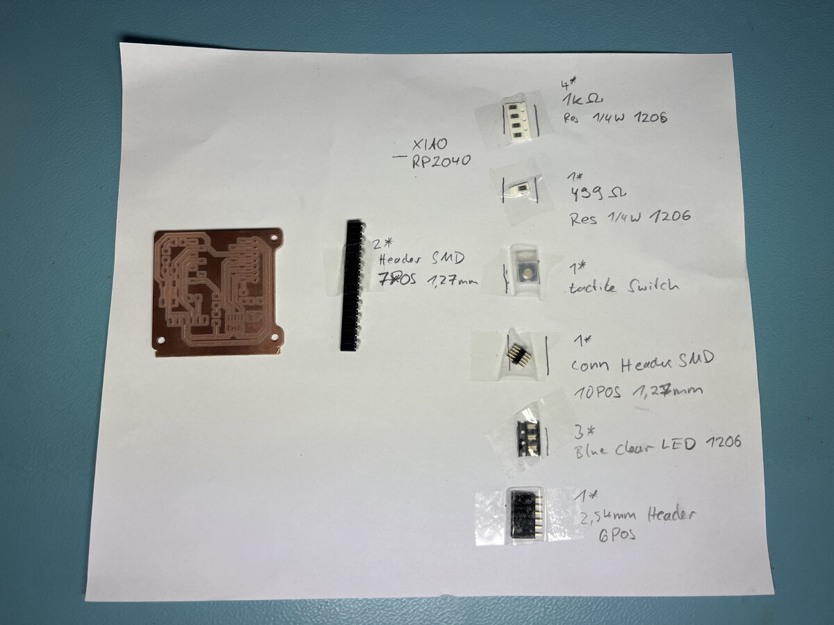 Before I started I searched for all the needed components and glued them on a piece of paper to keep track of them (and prevent loosing them).
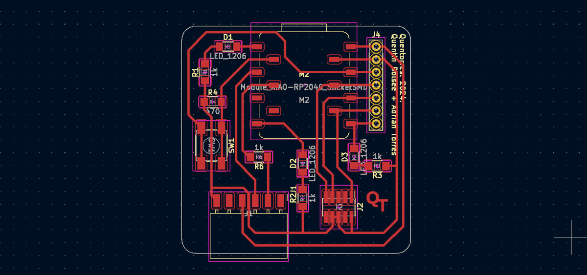
As a reference where to solder which components, I used the both pictures form the Instructor's Bootcamp website.
Soldering the 1206 components to the board is possible with a steady hand!

Final result
Self designed and manufactured PCBs
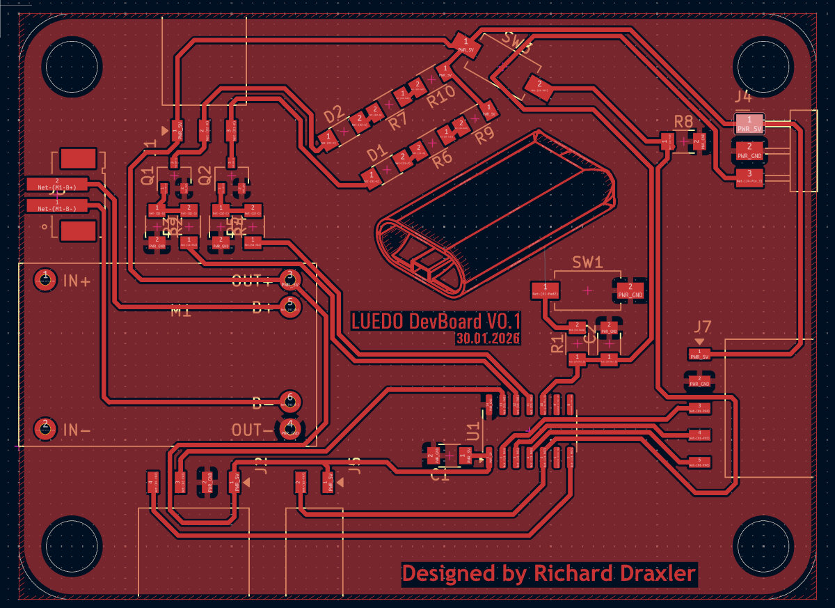
LUEDO DevBoard V0.1 (my first self designed PCB)
After milling the Quentorres programmer as a starter project it was time to produce my own PCB. I designed the PCB during this assignment: Electronics Design - Week06
Files
Images
LUEDO_DevBoard_V01_traces.svg
LUEDO_DevBoard_V01_traces.png
LUEDO_DevBoard_V01_Edge_Cuts.svg
LUEDO_DevBoard_V01_Edge_Cuts.png
.nc code
LUEDO_DevBoard_V01_0.15mill.nc
Manufacturing Process
In the first step, I mounted the PCB to the milling bed with double-sided tape.Then I tapped the board and mill with a multimeter and scratched the surface as already shown in the other PCB production above.
During the milling process, luckily no errors occurred and everything went fine. After about 20 minutes the board was finished and I could vacuum off all the accumulated dust of the board.
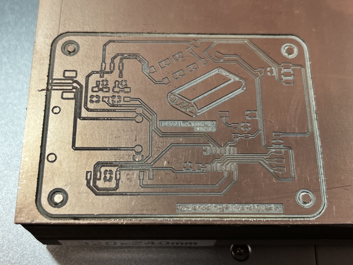
After removing the PCB from the milling bed, I started inspecting the quality of the milling process and was kind of unsatisfied due to the wrinkly surface of some traces. Even after sanding it with steel wool, it didn't get any better, so I switched to P400 sanding paper.
For checking the board, I set the multimeter to continuity mode and tapped the ground plane with one tip and the pads with the other tip. After some cleanup work with the scalpel none of the traces or pads were conducting to wrong places.
After all these steps, the board is now ready for assembly! I printed my bill of material as the useful guide for assembling the board. I need to modify some connectors from our inventory since not all width of the connectors were in stock.
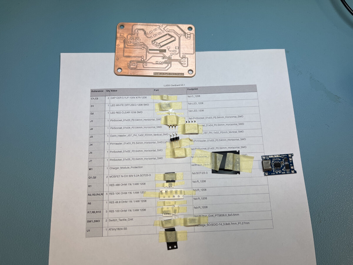
For the right placement of the components, I simply opened KiCad and showed just two layers, the copper layer, and the silk screen layer. With this information I could quickly figure out where to place e.g. R1,C1,... I started with the smallest components in this case, the capacitor, diodes, resistors and mosfets.
Generally, for the installation, I choose the normal tip of the soldering iron and not our soldering tweezers. My Method was to first solder the ground pad, and then the second part of the component. After the installation of the small 1206 components I moved onto the IC and the buttons. For the connectors, I decided to tin the pads first and then remove the solder with desoldering braid.
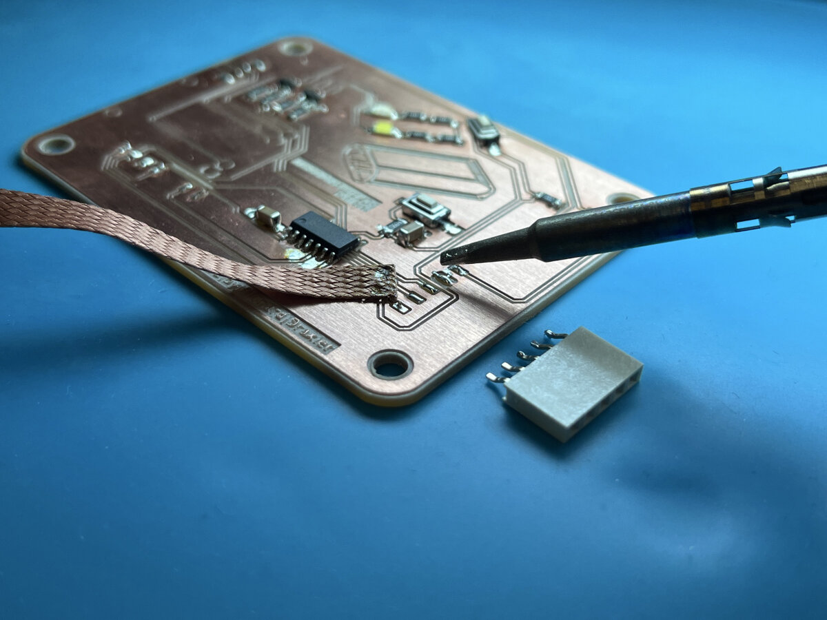
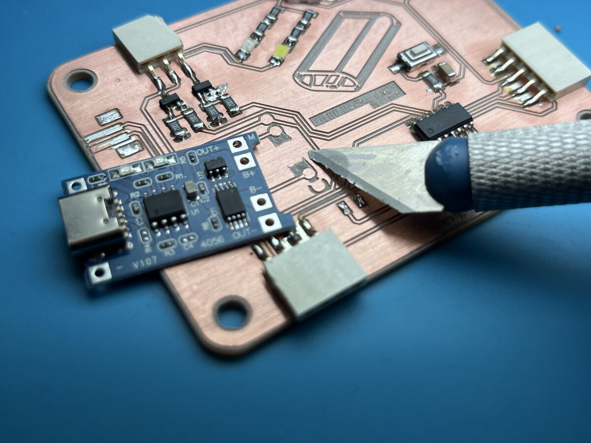
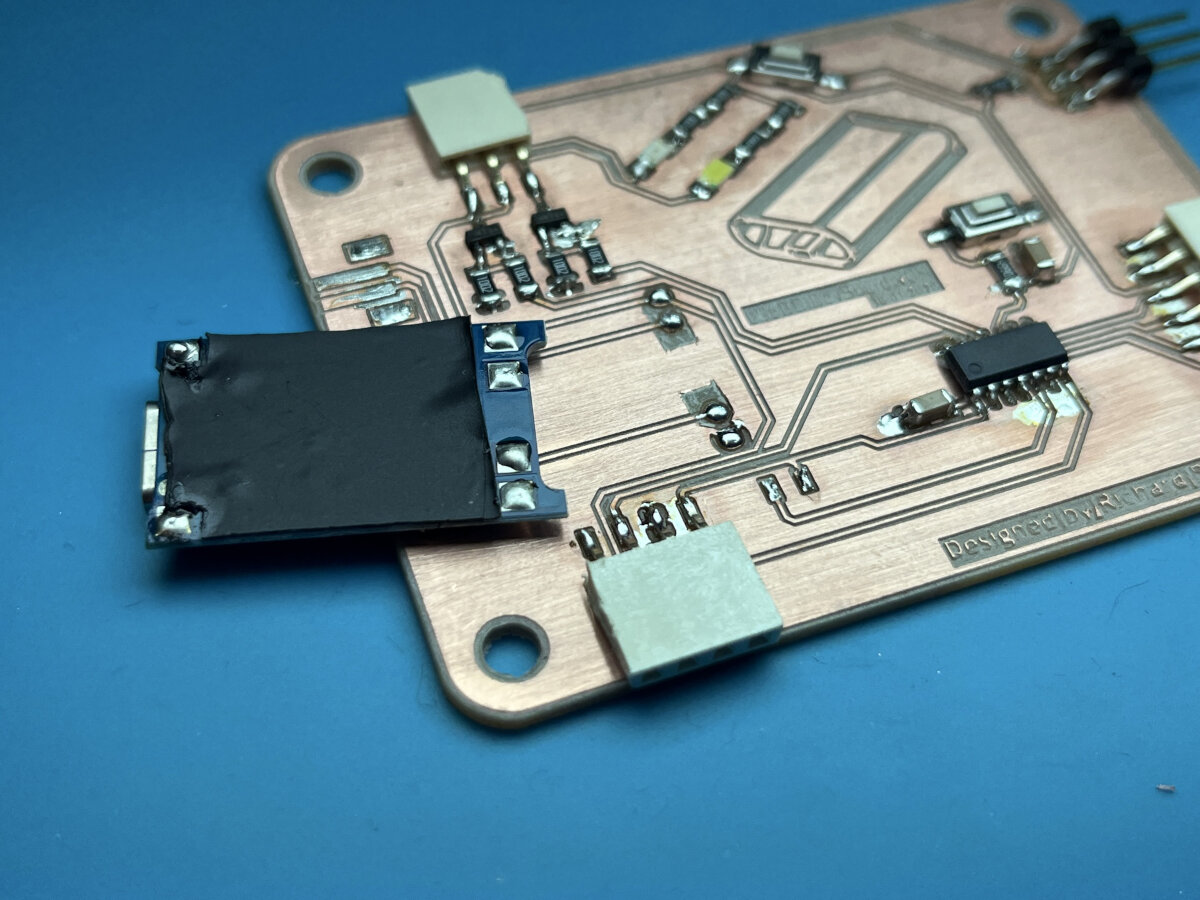
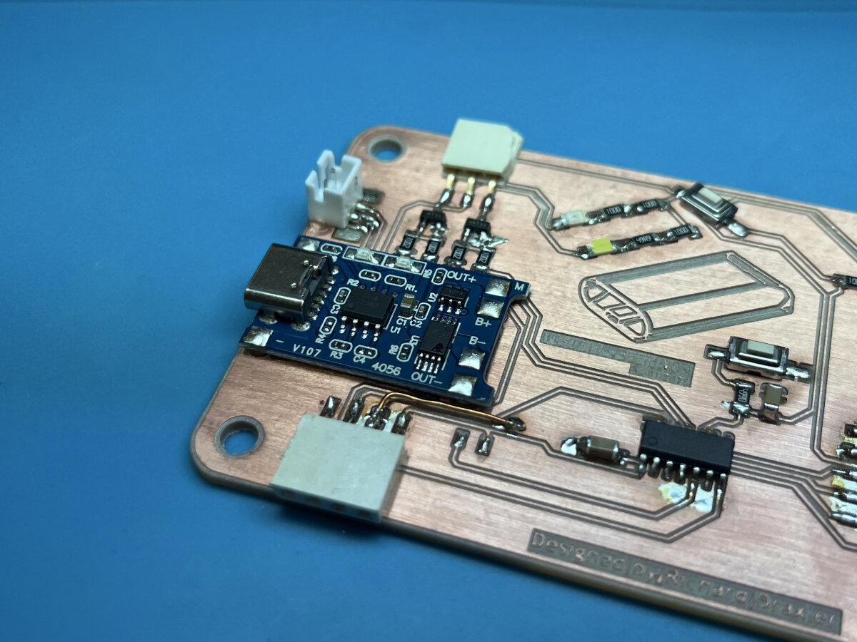
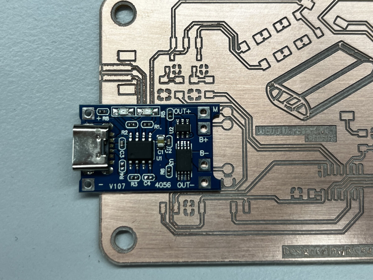
To install the TP 4056 by used the scalpel to remove some copper from the board which could possibly short to ground. Then I added the thick ball of solder to each pad to ensuring that the board is lifted a little from the GND pad. (This worked way better than I expected)
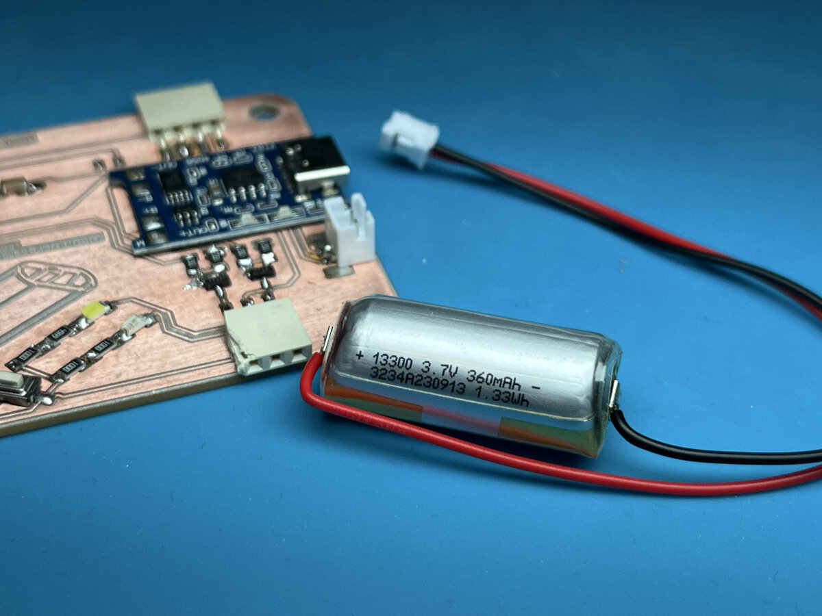
For the battery collector (JST), I only had a through-hole technology (THT) component, so I bent its legs to make it a surface mount component. To power everything for testing purposes, Ferdi recommended that we recycle batteries from single-use vapes. This gives a product that would otherwise be discarded a second life.
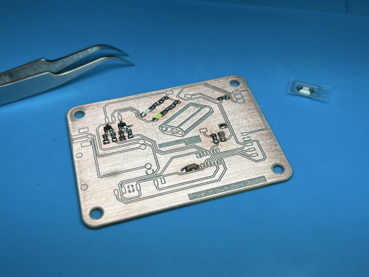
The last steps were a couple of repairs. On the lower side of the board I needed to bridge the missing ground pad, which got lost during the milling process. For this repair I used enameled copper wire.
The second issue that I fixed was a ripped pad under the battery connector. During first testing I already managed to rip off the complete battery connector from the board. I glued it back on with some superglue and added a few additional solder points.
Result
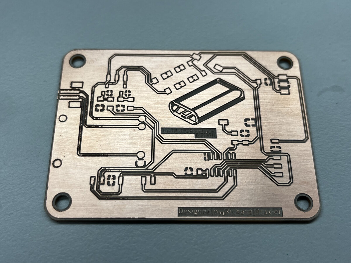
This is the blank board without components (after sanding with the steel wool)
I must admit I am very proud of the result, even tho it is not perfect. I am very happy the way it turned out, especially that the graphic is still visible and the overall shape of the board became what I envisioned.
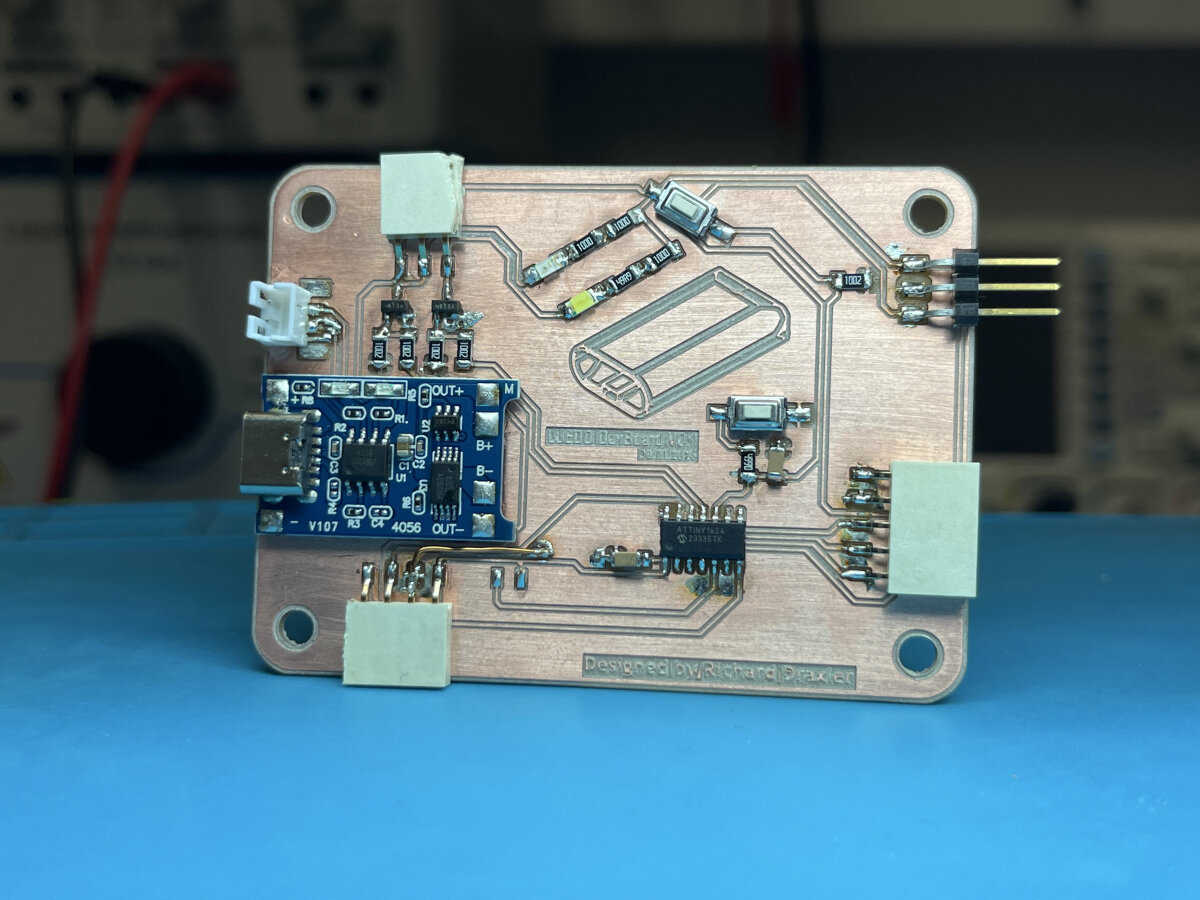
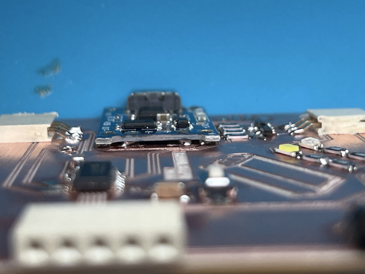
Fully assembled board with connectors, charging IC daughter board, AT1624 MCU, button and leds.
Fingers crossed that everything works as expected and that I am able to program the board!
Testing
I tested the board and documented the process in my embedded programming assignment.
Embedded Programming, Flashing ATtinys - Week04
Issues
...during the .nc code generation
In the beginning the images were different sizes, and therefore the traces overlapped with the edge cut.
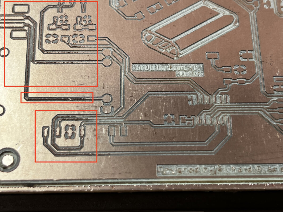
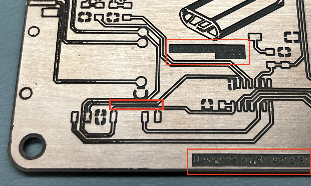
During the .nc code generation of the PCB I realized, that the text was too small and could not be milled into the board. Especially the text 'LUEDO DevBoard V0.1' and the lines of the Luedo glyph were below 0.2 mm line thickness. The text/graphic disappeared in the generated .nc file.
Even worse some pads were missing with the 0.2 mm setting.
Fix: Niclas form our FabLab recommended me to reduce the mill size for the traces down to 0.15 mm while generating. That fixed the issue, that some pads would not show up in the .nc code.
Nevertheless the board was milled with a 0.2 mm V-Bit, which resulted in narrower traces and smaller pads. Traces are now 0.35 mm instead of 0.4mm.
The mounting hole diameter is only 2 mm and not 2.4 mm as a proper thorough hole for M2 screws.
...during production
Some traces were uneven on the left side of the board.
This might be an issue related to an uneven milling bed.
Fix: Mill the bed flat with a large diameter bit (e.g. 6 mm flat end mill) before milling PCBs.
One part of the GND pad ripped of. In the original design it was only 0.2 mm. The text was to small as well, it ripped of.
Fix: Respect the minimal trace width and keep it above 0.254 mm.
...during soldering/assembly
After the board was post processed, I tried to lay out the large components and realized that I made an error in the footprint design for my TP 4056 charging module. I followed a YouTube tutorial for creating the footprint, but never checked my existing modules. Probably there is a second revision, which I currently have which has a slightly different pad layout. Therefore, I need to solder connection wires afterwards.
I ripped off the pads from the battery connector since it is too much pulling force perpendicular to the surface.
Fix:
- Use connectors with larger pads
- use connectors with horizontal pulling force
- add some superglue to secure the housing on the board
...during testing/programming
- use the right temperature on the hot air gun! At 400 °C the board starts pop-corning (300 °C worked just fine on another board)
- design a board with a dedicated +5 and GND measuring pads
- make sure programmer interface has reverse polarity protection
- design board with dedicated +5V and GND cable sockets
- superglue connectors/headers to the board for extra mechanical support
- check for clearance between components to avoid shorts
- additional capacitor might hinder programming the chip
- the output voltage of the TP4056 board is the battery voltage and not 5V as expected
Conclusion for the next boards
-
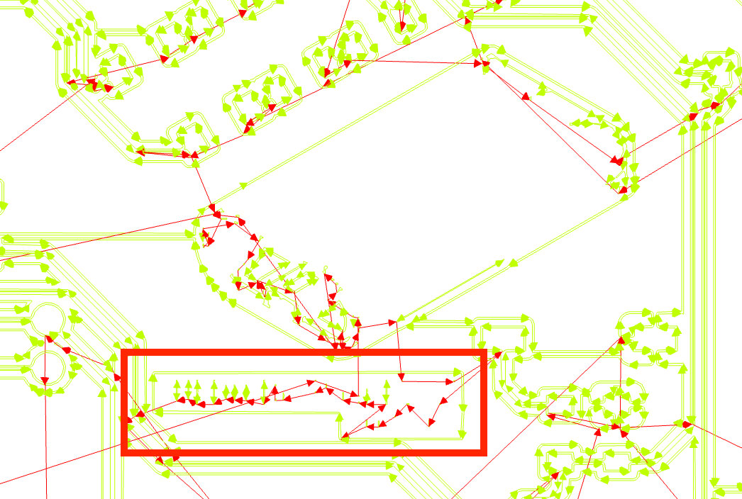
Surround the tracks more than twice, probably four or eight times to ensure that all the material surrounding the tracks will be removed to avoid little particles too short the board. This will help as well when components are not placed exactly in the right spot. For example a 1206 component which is slightly at an angle and automatically shorts to the ground pad.
-
Using as little as possible components speeds up the assembly process. Try to buy the appropriate resistors instead of soldering three different resistor values in the series.
-
Consider the program "remove all copper" to avoid any short circuits while soldering.
-
Increase the text size to a minimum of 0.4 mm thickness.
-
Make sure that the self-made footprints have drill holes if they are THT components.
-
For simple development or testing boards try to spread out the layout of the components to ease the assembly and the room for errors.
LUEDO LightBoard V0.1
Files
Result
Issues
UPDI Adapter
PERFECT use of space!
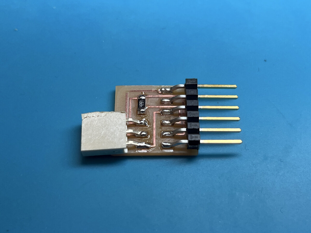
Finished adapter with 4.99kOhm resistor instead of 4.7kOhm resistor.
© 2026 Richard Draxler – Creative Commons Attribution Non Commercial
Source code hosted at gitlab.fabcloud.org