6. Electronics Design
view Checklists
*Checklist: personal*- [x] DeepL check spelling, grammar
- [ ] GPTcheck for better markdown
- [x] repair file links, replace .png -> .jpg; .mov -> .mp4 - [ ] remove file pathes from screenshots
- [x] clone and integrate FabAcademy KiCad Library
- [x] learn, KiCad tutorial on YouTube
- [x] design test board
- [x] finish schematics
- [x] create board layout
- [x] draw Luedo vector outline for board
- [x] create custom footprint for TP4056 Module
- [x] round edges
- [x] add Text to the board
- [x] design luedo mainboard
- [x] finish schematics
- [x] create board layout
- [x] design light board
- [x] finish schematics
- [x] create board layout
- [x] find right position for leds base on the reflector design
*Checklist: Nueval: Student's checklist*
- [x] Linked to the group assignment page
- [x] Documented what you have learned in electronics design
- [x] Checked your board can be fabricated
- [x] Explained problems and how you fixed them.
- [x] Included original design files (Eagle, KiCad, etc.)
- [x] Included a 'hero shot'
*Checklist: Task list Class/Nueval*
- [x] Group assignment:
- [x] Use the test equipment in your lab to observe the operation of an embedded microcontroller
- [x] Individual assignment:
- [x] Use an EDA tool to design an embedded microcontroller system using parts from the inventory, and check its design rules for fabrication
Learnings form the Group Assignment 
Link to our group assignment - week 06
Trace Width Calculator - AdvancedPCB
Trace Width Calculator - Multi-CB
Design Rules
I used a quick guide from Altium to learn the basics for PCB layouting rules. Die 5 wichtigsten PCB-Designregeln, die Sie kennen sollten (German)
EDA Tool: KiCad
(EDA - Electronic Design Automation)
For this week's assignment I choose the openSource option and installed KiCad. To learn KiCad I followed Ferdi's recommendation and watched the "Getting To Blinky 5.0" tutorial by Contextual Electronics on YouTube! This was a great course and on ramp for KiCad
Install KiCad
I used the latest version at the time: 9.0.1 for MacOS
Install the KiCad Library
For the installation I followed the official FabAcademy KiCad Library tutorial.
Warning! The library is under active development. Naming of components can change overnight. Make sure to
git pullthe latest version before doing work.
- I cloned the repo into my
Documents/KiCadwithgit clone git@gitlab.fabcloud.org:pub/libraries/electronics/kicad.git - Renamed the folder to
fab - Open KiCad in the main window do not open a schematic or PCB design
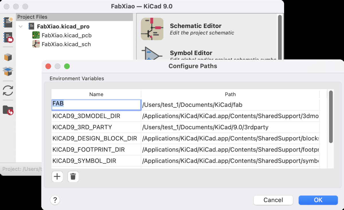
- Go to 'Preferences' → 'Configure' path
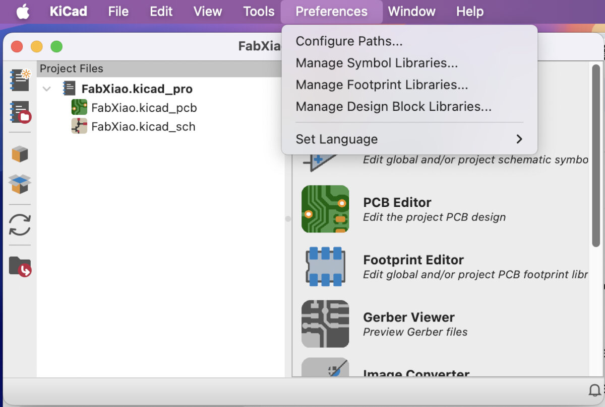
- Add new environment variable "FAB"
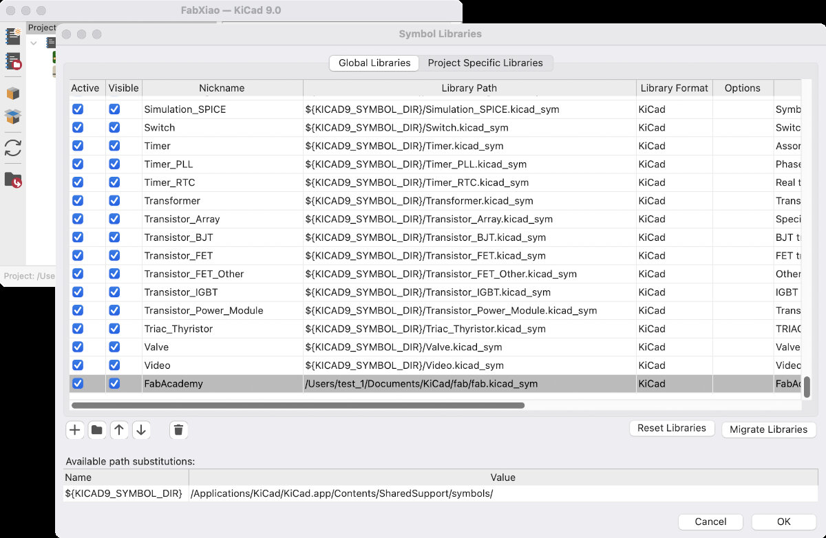
- Go to 'Preferences / Manage Symbol Libraries' and add fab.kicad_sym as symbol library.
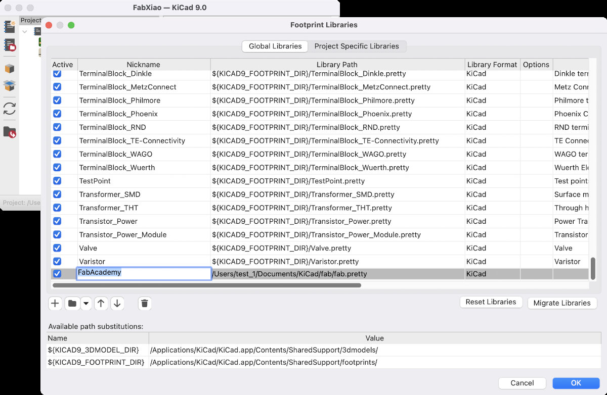
- Go to 'Preferences / Manage Footprint Libraries' and add fab.pretty as footprint library.
- Restart KiCad and check in the schematics editor if FabAcademy library is available
Bugfix with the Fab KiCad Library:
I had the following problem: When I placed a component, it didn't load the right footprint for the component.
Jakob recommended to me to simply delete and reinstall the libraries which fixed the issue for me and successfully selected the right footprint for the assigned part. That saves me a ton of work.
The Basics - getting started with KiCad
Shortcuts and functions of the software
Schematics
general notes:
- Power Flags can define lines as power lines
- no connect X clears error messages in ERC
Schematic Editor
crate and edit your schematics
| Shortcut | Description |
|---|---|
| A | Place component |
| E | Symbol properties / additional info |
| Cmd+D | Duplicate component |
| V | Value for component |
| W | Route a wire |
| L | Label a wire (while wire is selected) |
ERC - Electrical Rules Checker
- Are all pins connected?
- Is everything annotated?
Annotate Schematic
Can automatically annotate your schematic
Symbol Editor
crate your own symbols or edit existing ones
| Shortcut | Description |
|---|---|
| M | move |
| R | rotate |
| E | edit object |
Assign Footprints
Filter and search for component footprints
Update PCB from Schematic
- Checks if all components have assigned footprints
- F8 - opens window "Update PCB from Schematic"
Footprint Editor
'File' → 'new Library' (keep them in the project and not global, otherwise they are visible everywhere)
right click → Grid, to change grid size
Cmd+Shift+M - Measurement tool
Space - reset dx and dy coordinates
PCB
General Notes
| Layer | Description |
|---|---|
| F | Front side of the PCB |
| B | Back side of the PCB |
| Edge.Cuts | Defines the outer perimeter of the board |
| Fab | Fabrication layer; provides information for the manufacturer (not printed on the board) |
| Silkscreen | Annotation layer; visible paint on the PCB for labeling and marking |
| Courtyard | Forbidden area for component placement |
| Paste | Solder paste layer; used for designing stencils |
| Abbreviation | Description |
|---|---|
| PTH | Plated Through Hole (via) |
| NPTH | Non-Plated Through Hole (via) |
PCB Editor
General
press "Update PCB from schematic" or press F8 to transfer exiting schematic to the PCB workspace
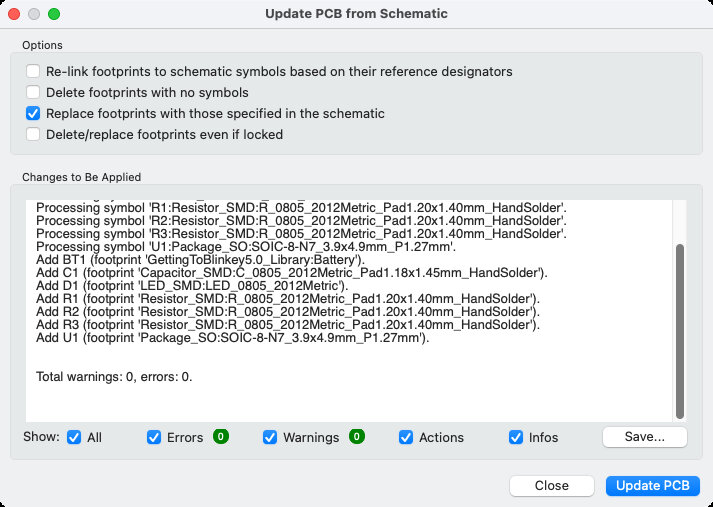
Note
If the "update PCB from schematic" button is not available there is no project file or the main Kicad instance is not running. Close all and restart the project from the .kicad_pro file, the button will appear.
Possible warnings inform you about missing pads or parts without footprints
| Shortcut | Description |
|---|---|
| F | move part to front or back side |
| R | rotate |
| M | grab and move |
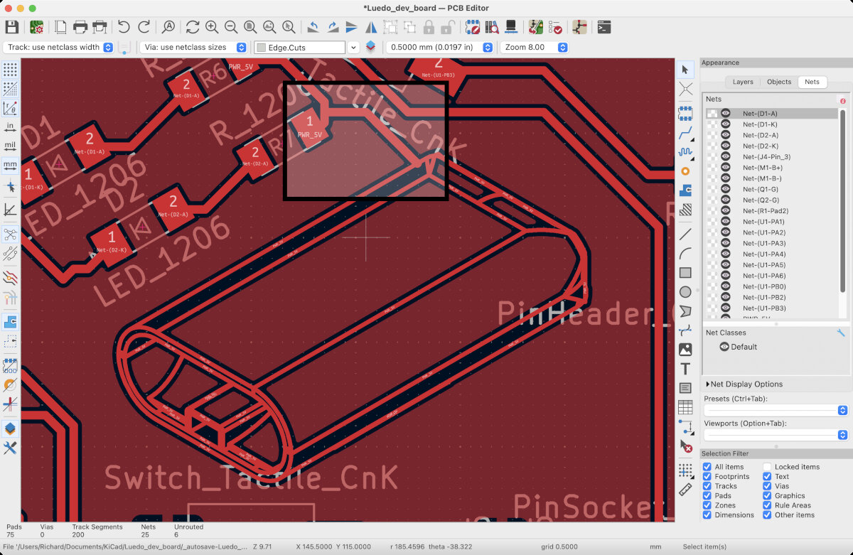
Nets (right hand panel)
Nets Classes - hide/view Ratsnest (floating connection wires)
Tracks
| Shortcut | Description |
|---|---|
| T | Find part in the PCB viewer |
| X | Start a track (make sure copper layer is selected; adjust grid first for snapping) |
| V | Place a via while drawing a track |
| D | Select a track and drag |
| I | Select part of a track; pressing 'I' shows the rest of the track |
| Draw Filled Zones | Create a copper fill layer; useful for full GND or VDD planes |
| B | Calculate/show/update the ground pad |
| E | Edit, opens 'Copper Zone Properties', setup clearance, thermal reliefs, ... 'Electrical Properties', set the clearance of the filled zone |
Cross-referencing
Cross-reference between schematic and PCB editor
Board Setup
- defaults usually work fine
- change/edit design rules base of the parameters which were determined during the group assignment
- define minimal track width and minimum clearance
- or define the clearance and track width in the NetClass
Edit Text and graphics properties
'Edit' → 'Edit Text and graphics properties'
to edit the visibility and properties of any text on the board
View
Alt+3 - open 3D PCB viewer
View → flip Board
V - switch layers
DRC - Design Rule Check
first create and set up the needed rules in the 'Board Setup' menu
Export for Production
Milling
This process can be found in the assignment Electronics Production Week08 - KiCAD to PNG
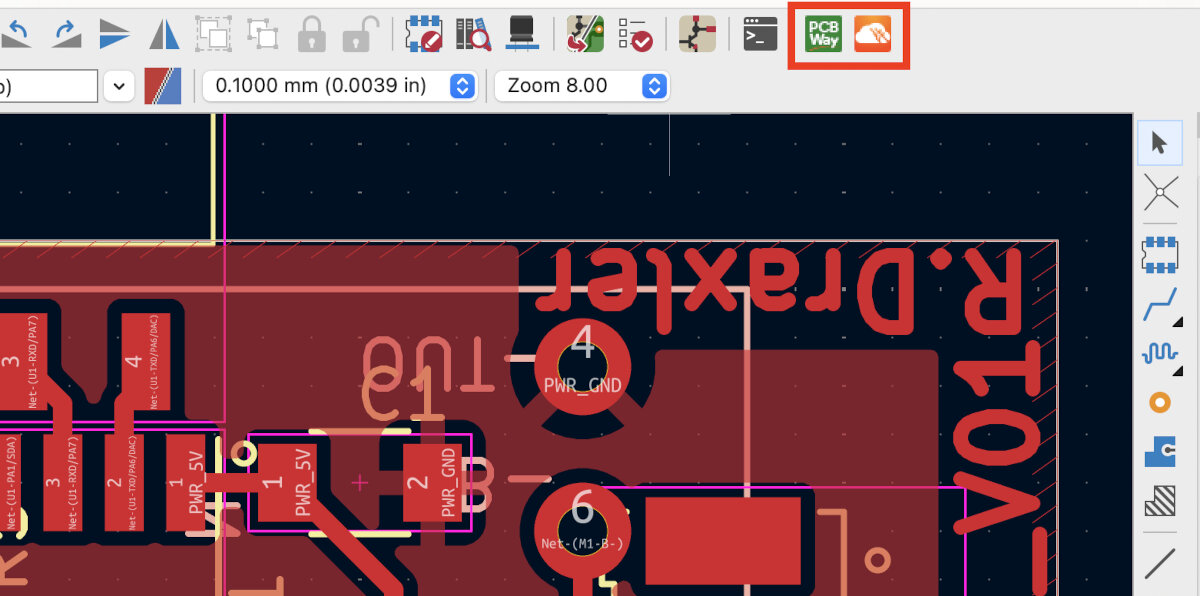
Board Houses
I have not used any board houses yet, because everything is manufactured locally.
There are several plugins for KiCad to ease the export for board houses.
- In the KiCad main window go to "Plugin and Content Manager"
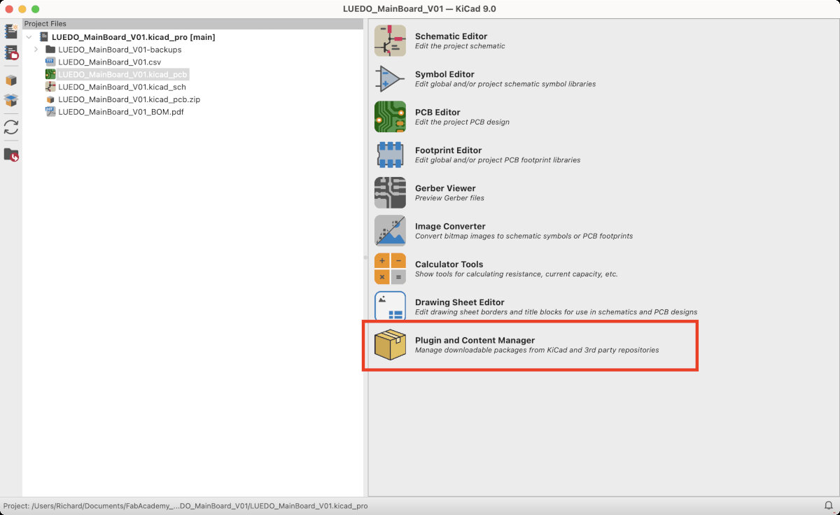
- Go to Fabrication plugins, and install the desired plugin.
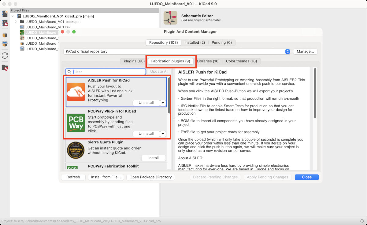
- Now the plugins should be visible in the PCB Editor!
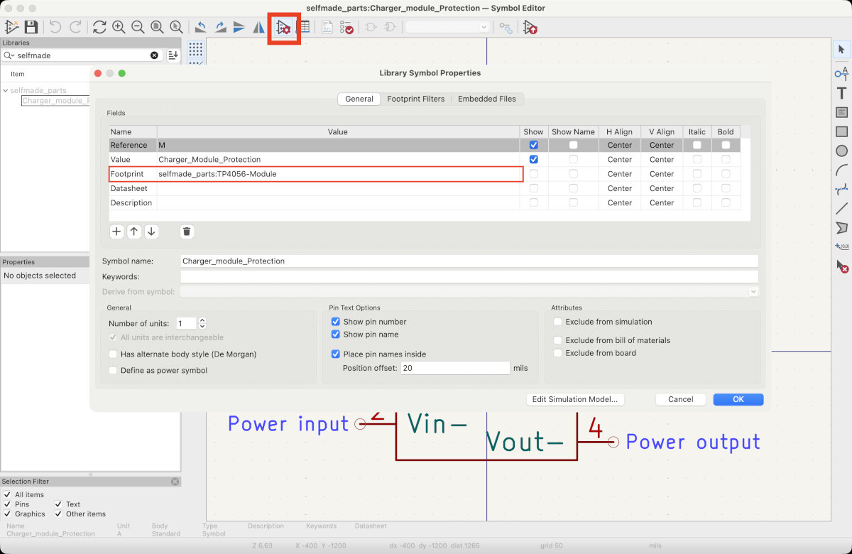
Custom Parts: Schematic, Footprint, 3D Model
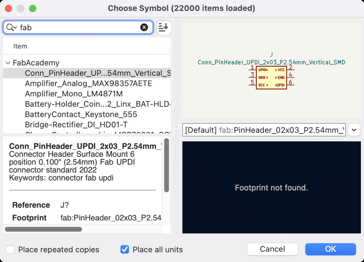
For my application I needed a custom component for the TP4056 board. Therefore, I followed a TP4056 tutorial on YouTube to recreate the part. Every component consists of tree files:
Symbol: TP4056_kicad_symbol
Footprint: TP4056_kicad_footprint
3D File: TP4056_kicad_3dshape
For the 3D model I downloaded the model from GrabCAD TP4056 Charging module - GrabCAD.
Steps for a custom part:
- Open the Symbol Editor, create new library or choose a symbol library where the new component should be created in. I created my own symbol library called 'selfmade_parts'.
- Create a new symbol and recrate the part as shown below.
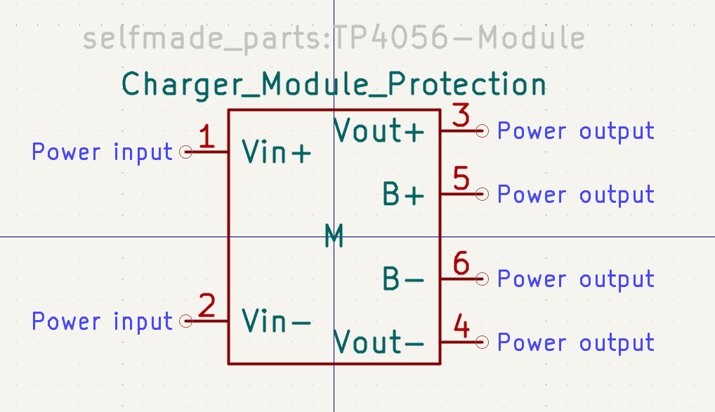
- Save new symbol.
- Open the Footprint Editor, create a new footprint library. I created mine called 'selfmade_parts'.
- Recreate the footprint as shown in the video (TP4056 tutorial on YouTube) or shown in the screenshot.
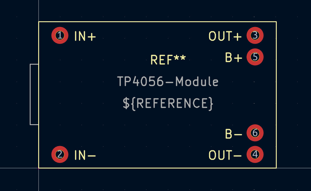
- Save new footprint.
- Open Symbol Editor and link the footprint to the symbol.
My Boards
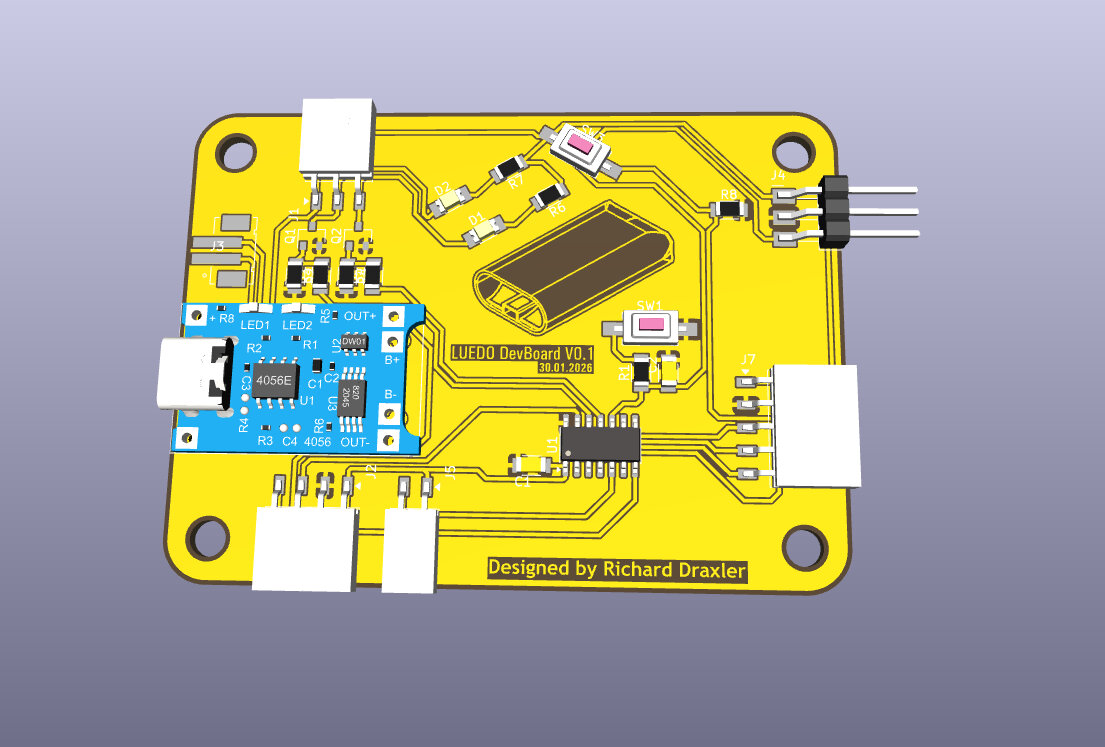
LUEDO DevBoard V0.1 (My first board)
My first board - simply produce Quentrorres for later programming ATtiny's
Requirements, Notes, Block Diagram
The LUEDO DevBoard V0.1 should be used as a general prototyping board to emulate the operation of the Luedo lamp which I am working on in my final project. Before the FabAcademy I already tested a basic circuit with an Arduino Uno and a breadboard.
The DevBoard is designed to demonstrate the implemented functions. The circuit and software design are not optimized for power efficiency, footprint, security or price.
First step was to create a block diagram, which gives a rough overview of the components and board components.
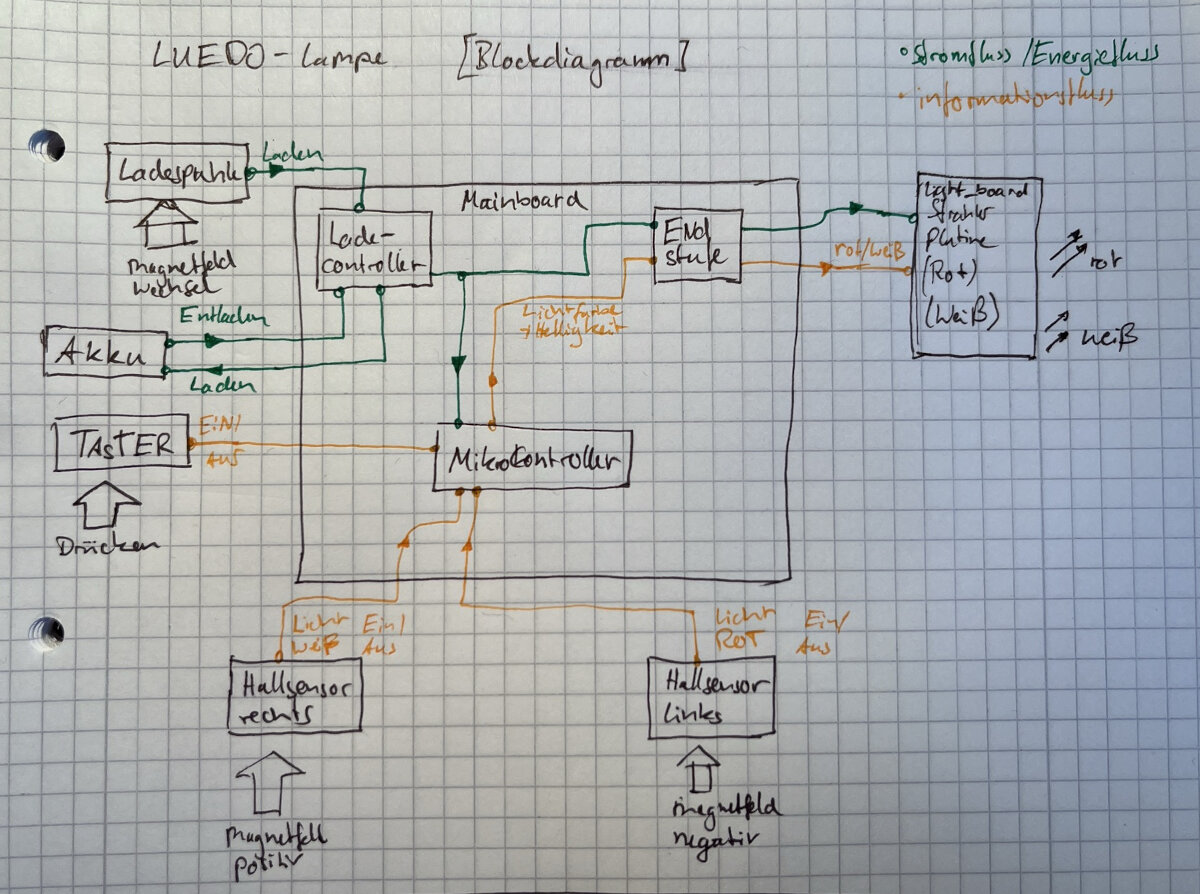
For the DevBoard_V0.1 I had the following requirements
(optional/future features are marked italic)
Components:
- ATtiny 1624
- UPDI programmer connector
- configured with a 3pin interface to work with the Quentorres programmer and UART to UPDI + VCC connector
- 2x hall sensor connectors
- 2x buttons for emulation
- Power LED board connector
- USB-C power connector
- Battery connector for LiPo cell
- Battery changing circuit
- LiPo USB-C interface board
- Button (main LUEDO button)
- Mosfet for LED driver
- N-Channel
- onboard white and red LEDs for emulation
- connector for spear IO
- connector for LED array
- connector for IR reflection sensor
Power rails:
- GND
- +5V
- +12V or +9V
Mechanical:
- four mounting holes for M3 screws
- rounded edges
- Text: LUEDO DevBoard_V0.1
- Text: Richard Draxler
- Text: Date
- Logo glyph of the Luedo light
Configuring MosFets
Transistor Tutorial Summary - electronics-tutorials.ws
MOSFET as a Switch - electronics-tutorials.ws
To drive the high power main LEDs I needed a Mosfet. I did some basic research about mosfets here
depletion vs enhancement
- depletion: always on (conductive)
- enhancement: always of (not conductive)
N-Channel vs. P-Channel
N-Channel:
- positive input voltage
- extremely high input resistance
- two modes: enhancement-mode and depletion-mode
- positive voltage needed to turn on (e.g. +5V)
- no voltage to turn off (e.g GND)
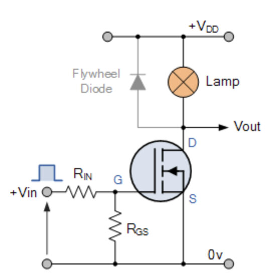
For my application I need a depletion, N-Chanel mosfet.
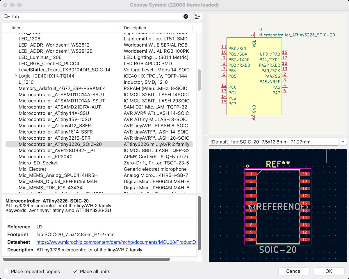
Before I started to implement the schematic in KiCad I decided to draw it by hand, while researching the needed pieces from the ATtiny 1624 datasheet.
Schematic Design
Steps
-
In the beginning I added the ATtiny1624 and the capacitor to prevent frequency interference. Additional details in Embedded Programming Week04 - ATtiny 1624 Datasheet Notes
-
The reset circuit was shown in the datasheet, that's why I copied the circuit to my schematic. Additional details in Embedded Programming Week04 - ATtiny 1624 Datasheet Notes
-
The Mosfet circuit was not in the datasheet since it is an application specific circuit, which is targeted for a specific use case. For finding the right mosfets I first did some research on the application of mosfets. The specific mosfet that I choose was the 'MOSFET N-CH 30V 5.2A SOT23-3' from the FabInventory.
I added a white LED and a red LED as a signal LED to the board to make the board already fully working without peripherals (sensors and leds). For the series resistance of the LED I choose to run both LEDs at half current to keep them dim.
For the calculation of the resistor I used the \(R=U/I\) formula.White (@3.3V @10mA): 170Ω
Red (@2V @10mA): 300ΩThen I realized there is not enough space for multiple resistor to reach the exact value, that's why I adjusted the results based of the existing FabInventory resistors.
With \(I=U/R\) I got the following results:White LED with a 100Ω and a 49,9Ω resistor: White (@3,3V @11,3mA)
Red LED with two 100Ω resistors: Red (@2V @15mA) -
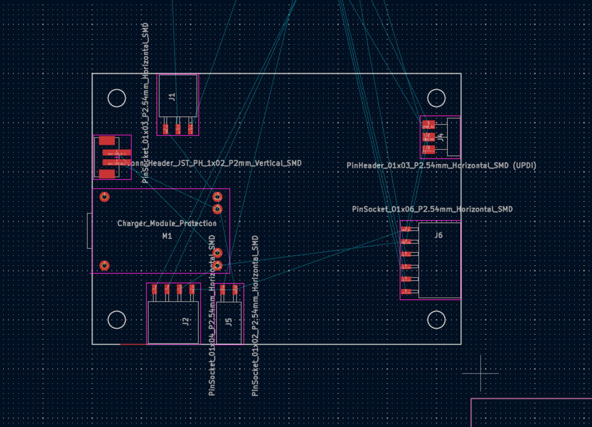
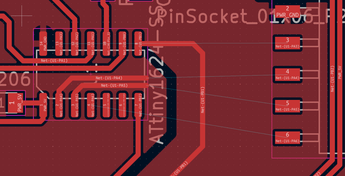
For the UPDI connector I used 6pin horizontal socket in the first version, to replace it later with the 3pin version which is compatible with the Quentorres programmer and UART to UPDI + VCC connector
-
Hall sensor connector:
For the interface I chose a horizontal 1x4 socket to connect to the SensorBoard. In the Input devices Assignment - Week 09 I documented why I chose the simple analog hall sensors. This sensor needs a +5V, GND and Signal connection. -
Lipo charging circuit:
To embed a custom safe charging circuit for Lipo batteries I decided to use of the shelf parts and design a custom part/footprint for the TP4056 charging module. The Battery is connected with a JST-PH header. -
Main button:
For the main button I used a tactile switch with a pull down resistor (10 kΩ). -
Spear I/0:
Since the Microcontroller has multiple unused i/o ports I decided to connect them to a header to make the board useable for other purposes later. -
Adding component values:
The last step was for me to add all the component values to later crate a Bill of Materials - BOM. I tied to use many identical components, to ease the assembly process.
Schematics File, Final Result
This is the schematic:
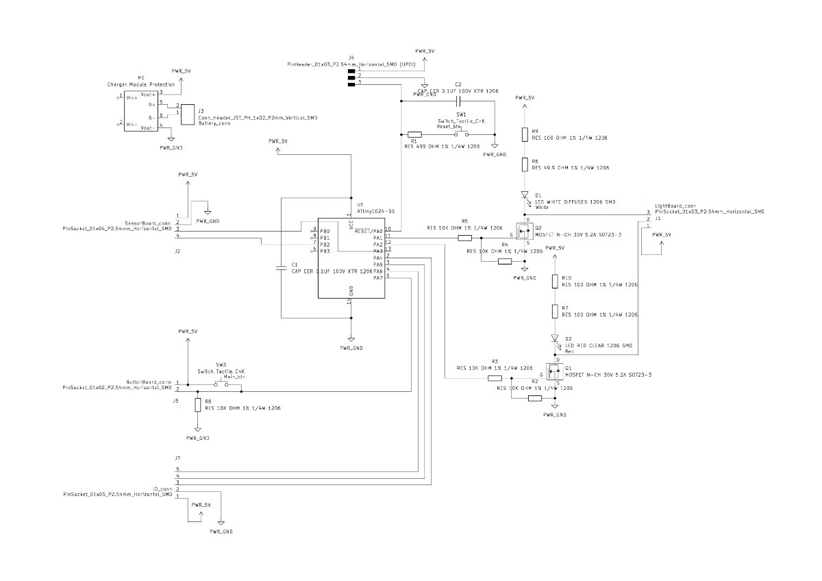
Schematic for the LUEDO DevBoard V0.1.
The .kicad_sch file can be opened in KiCad.
LUEDO DevBoard V0.1.kicad_sch
the project file can be found below
Board Design
I started with a quick sketch to ensure the right size of the board. I choose the outer size of the board to be 75 mm x 55 mm. Our labs normal stock size is 120 mm x 80 mm, therefore the board can be manufactured twice if an error occurs during production.
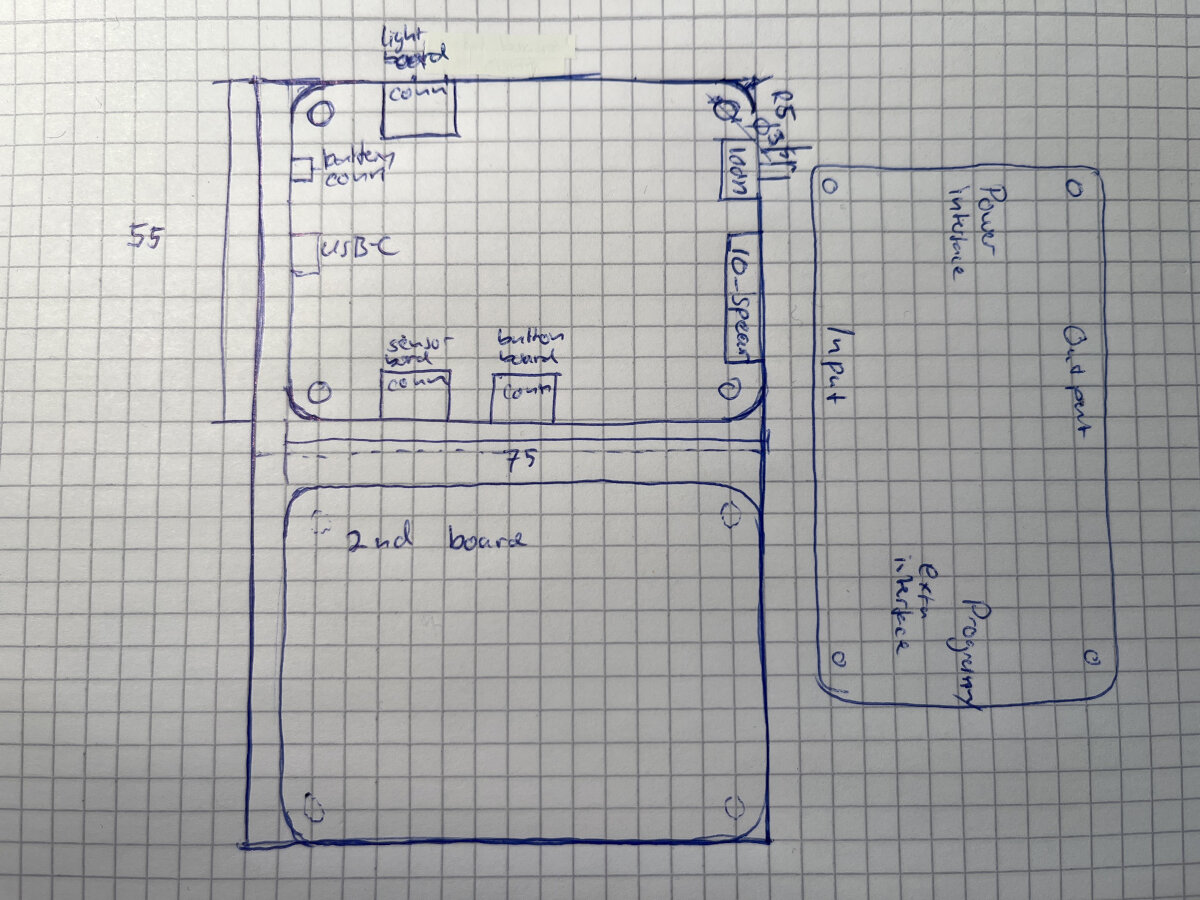
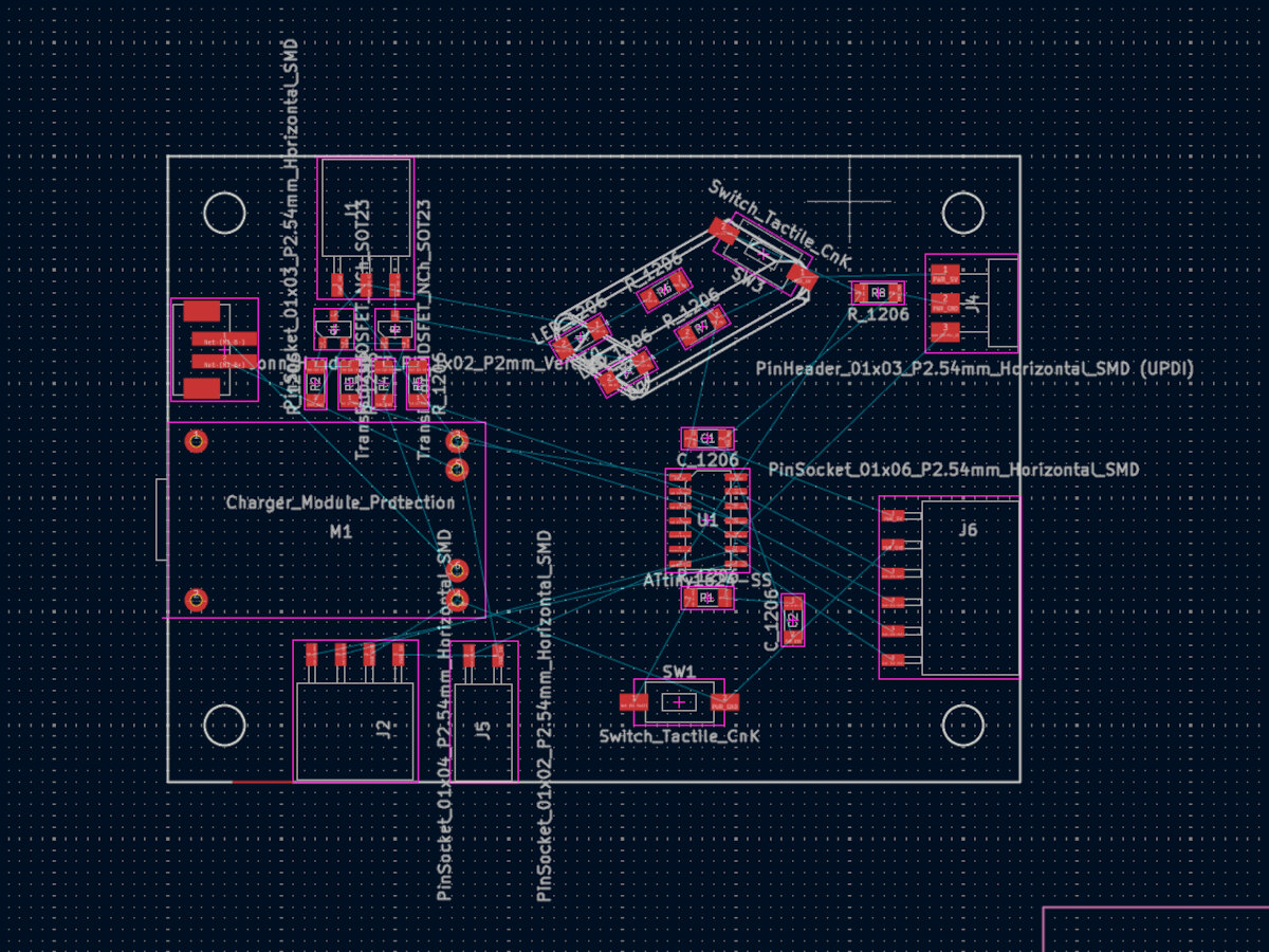
Placing Components
-
In the beginning I placed just the connectors and the large components according to my sketch.
-
I placed the microcontroller and the adjacent capacitor and reset switch.
-
Placing mosfets and resistors.
-
For the lamp simulator I took a screenshot of my Luedo shell in Shapr3D. Afterwords I vectorized and cleaned up the glyph in Inkscape. I exported the file as a .dxf to later import the
LUEDO_glyph.dxf into KiCad.
After the PCB was finished I realized I needed to move the glyph to the F.Cu layer to make it visible on our milled PCBs. To move a graphic to another layer got to 'Edit'->'Edit Text and graphics properties'
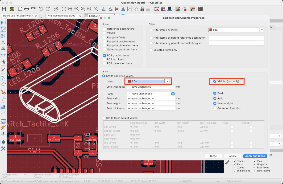
Connect Graphic to Net
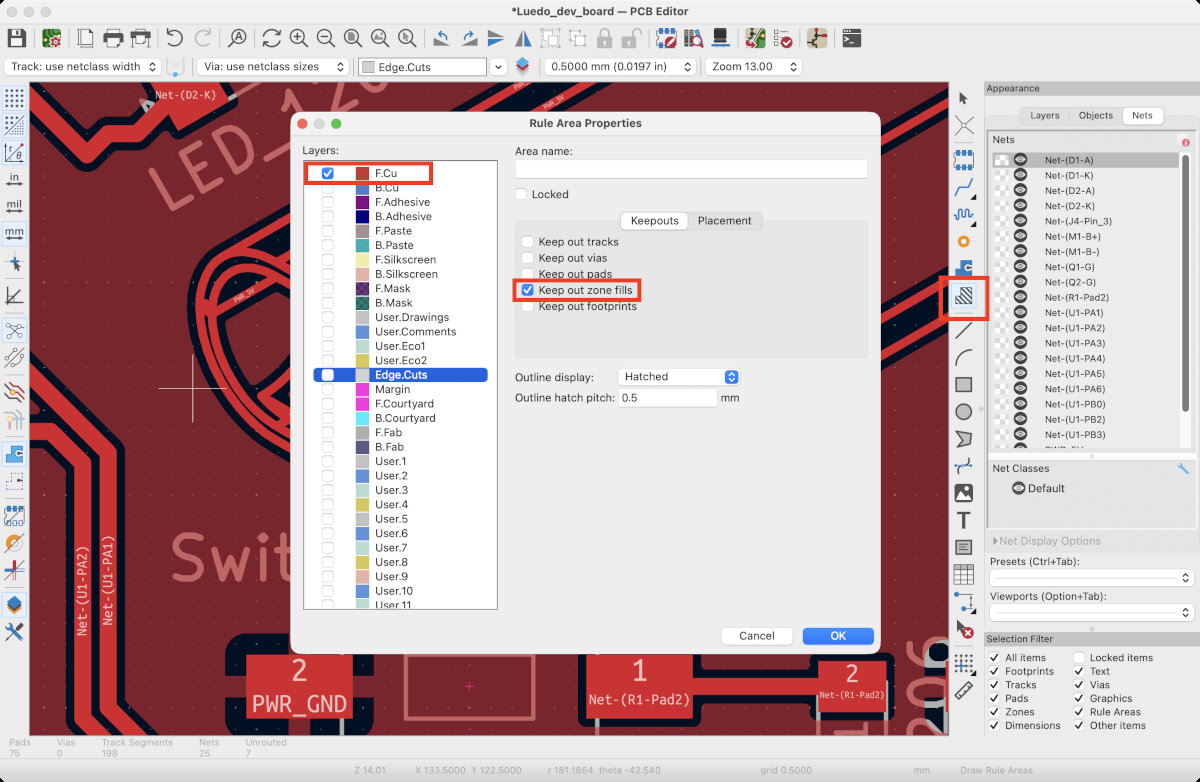
While transfering the graphic to the F.Cu Layer the it must already overlap with the +5_PWR net, only then it will be excluded from the GND plane. After rendering the filled zone with 'B' the connection tack to the 5V line can be removed, because then the graphic is already assigned to the 5v_PWR net. (source: Connect polygon to net - KiCad Forum)
Disable the GND plane in a defined area
To remove the filling inside of the graphic, a 'Ruled Area' can be used to block the GND plane from filling the inside of the assigned area.
Routing Traces
The appropriate design rules for my board were defined by the parameters found in the Electronics Production - Week 08.
I needed these parameters for my own board.
Here are the design rules defined by the milling test in the Electronics Production - Week 08 assignment.
Traces
min. trace width: 0.01" (0.254mm)
typ. trace width: 0.4mm
Clearance between Traces
min. clearance between traces: 0.007" (0.1778mm)
typ. clearance between traces: 0.2mm
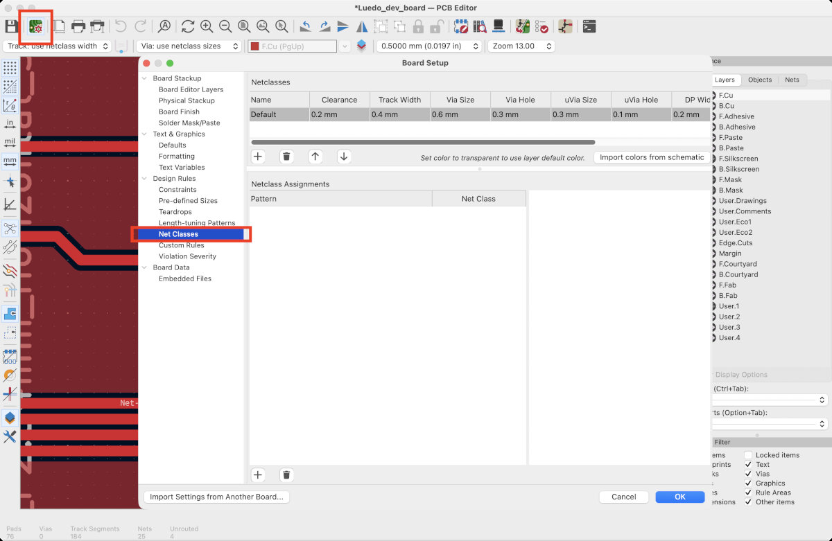
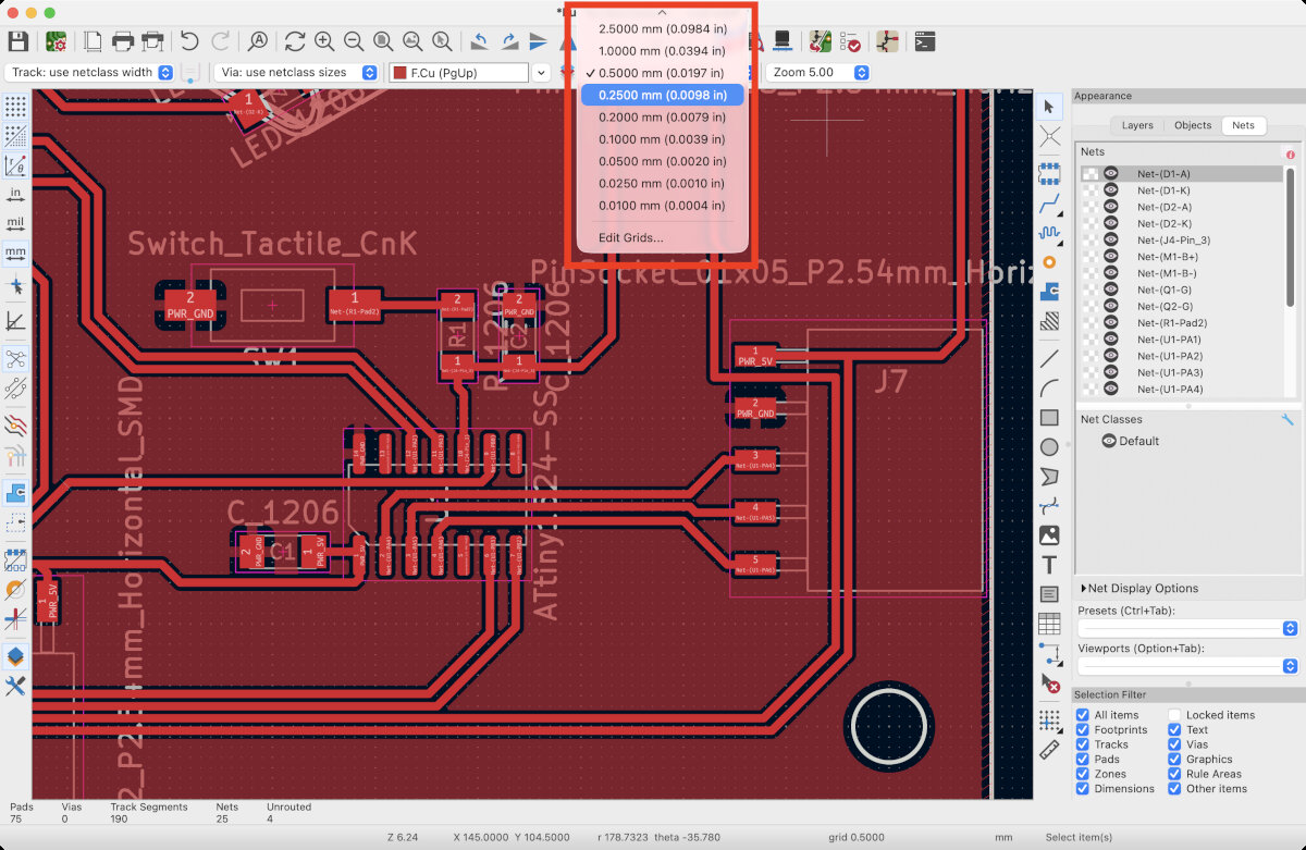
In KiCad the trace width and parameters are defined in the Net Classes which can be found in 'Board Setup' -> 'Net Classes'. Here I inserted the values form above (I choose the typical values).
Ground Plane
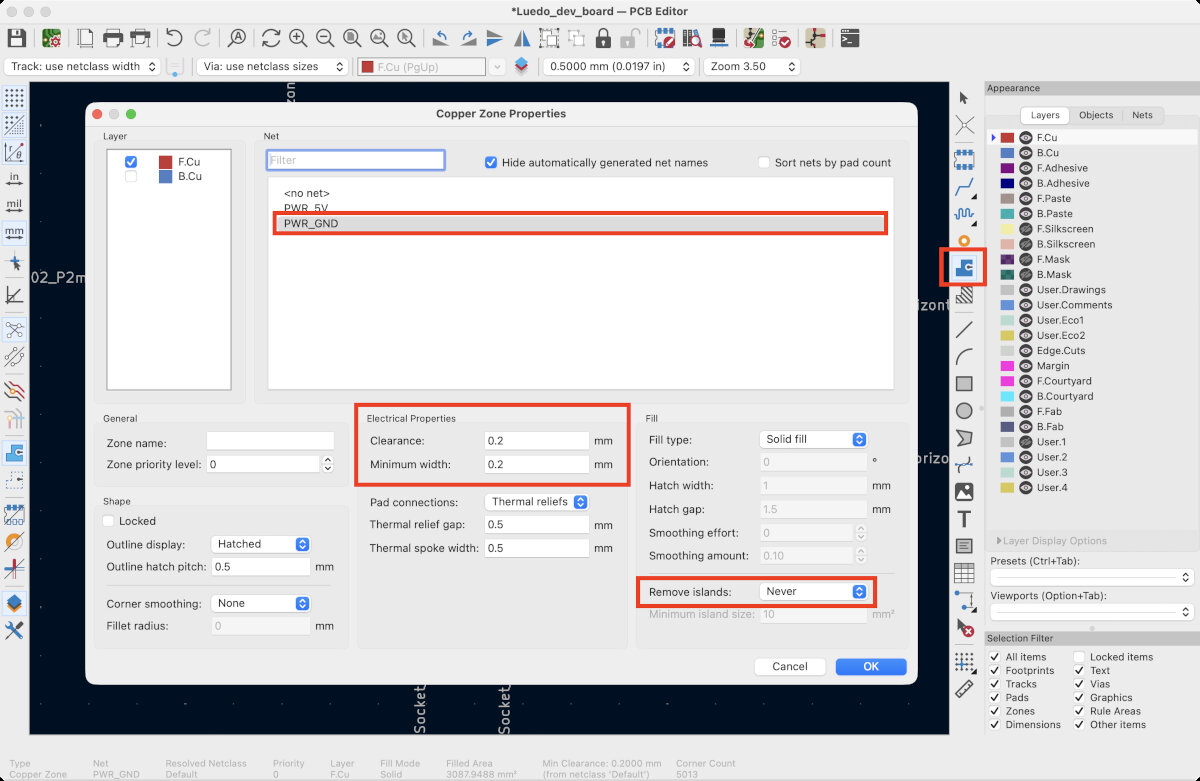
I used the 'Draw Filled Zones' tool to create a GND plane and kept all the islands (this should reduce the milling time in the end, since fewer material needs to be removed)
Adding 0Ω Resistors/Bridges
My issue was that most of the remaining Microcontroller lines would overlap in the PCB design. Fort that reason I decided to change some connections in the schematic to avoid bridging traces.
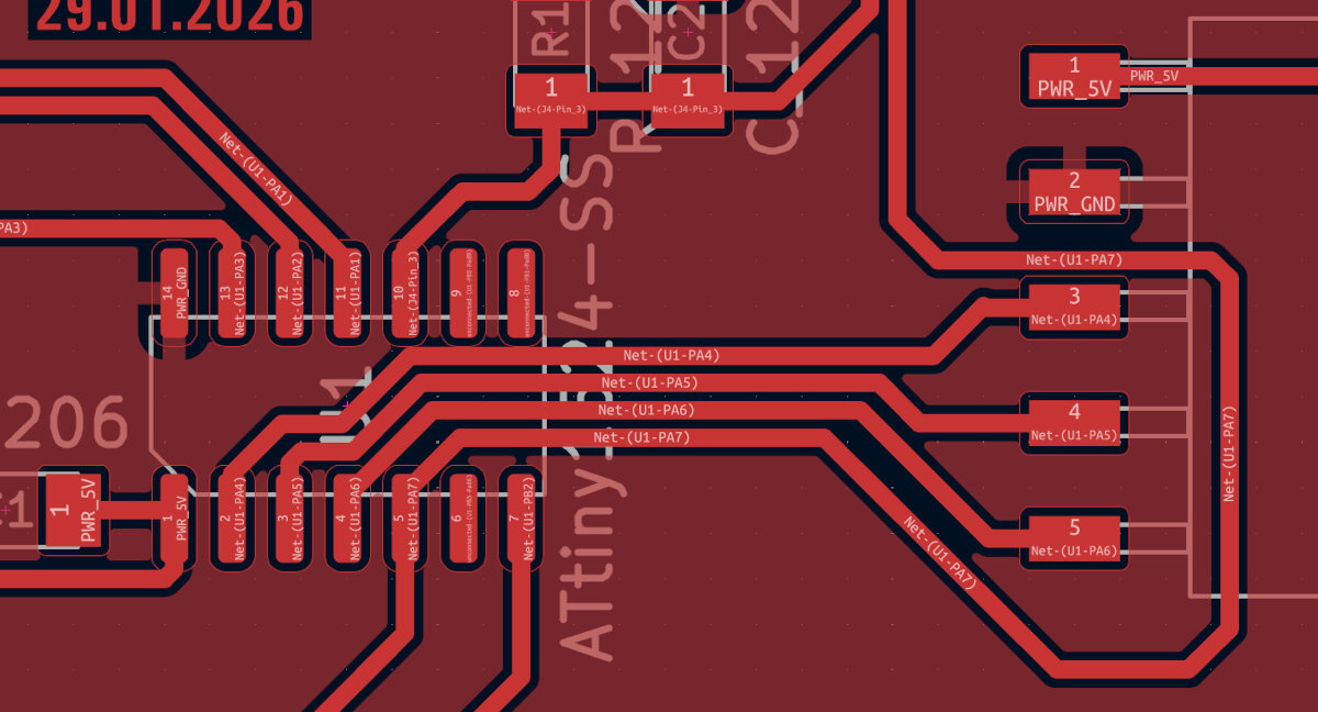
After changing the pins in the schematic I managed to avoid bridging. In the beginning I thought I need many bridges, but in the end I could route the design without any 0Ω resistors.
Note
I removed one of my spear I/O beakout pins because tree are enough as a backup, four are not needed for this board.
Text, Styling, Edgecut
The last step was to add the Text to the board. I added the version number, the date and my name. During the layer switching of some of my graphics, the edge cut got lost, and I created a new edge cut with rounded edges and 2 mm mounting holes for M2 screws.
Note
During the .nc code generation of the PCB I realized, that the text was to small and could not be milled into the board. Especially the text 'LUEDO DevBoard V0.1' and the lines of the Luedo glyph were below 0.2 mm line thickness. The text/graphic disappeared in the generated .nc file
Design Rule Checker
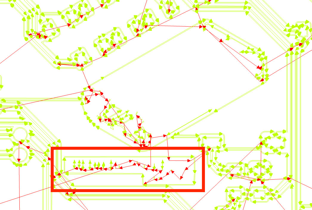
For validating and iterating on my design the DRC was a very useful tool which helped my to find missing connections in my layout. I checked all the markers which appeared on my board and fixed the issues.
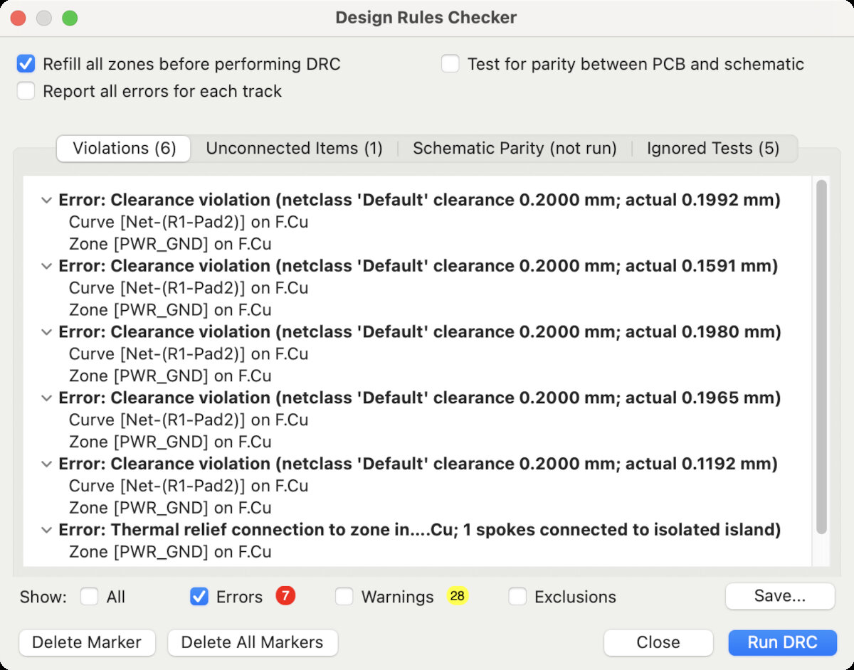
Some markers were not relevant for my application, that's why I ignored thermal errors.
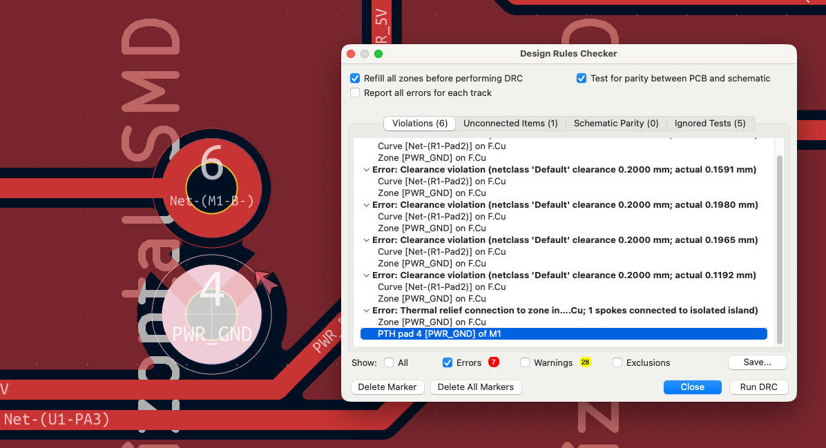
I ignored all the markers that appeared next to my Luedo glyph, because this is not a functional part of my layout.
PCB File, Final Result
This is the final result!
The .kicad_pcb file can be opened in KiCAD.
LUEDO DevBoard V0.1.kicad_pcb
the project file can be found below
Bill of Materials - BOM
For the assembly, cost calculation and planning it is very useful to have a bill of materials. The BOM is created automatically in the background and is saved as a .csv file.
The .csv can be opened in any kind of spreadsheet software.
LUEDO DevBoard V0.1.csv
the project file can be found below
Conclusion on the design Process for my first PCB
- routing traces in the end is the hardest
- keeping a clear schematic and tidy PCB layout is not easy
- before placing any components check your grid size and keep it always the same to avoid weirdly short tracks.
- routing traces feels a bit like a game
- its fun
- my pcb needed no bridges, I am very proud of that
Design Files
The design files are linked in their corresponding sections as well.
Project file:
LUEDO DevBoard V0.1.kicad_pro
Design files:
LUEDO DevBoard V0.1.kicad_sch
LUEDO DevBoard V0.1.kicad_pcb
LUEDO DevBoard V0.1.csv
LUEDO MainBoard_V0.1
... in comparison to DevBoard_V0.1
- switch to ATtiny 412
- remove reset circuit and buffer capacitor
- remove onboard LEDs and button
- make the battery connector a THT component next to the TP4056 board
- consider using flat ribbon cables and FPC connector → to large in 4pin config (11 mm wide, 6 mm high, 75 mm deep)
- use solder pads instead
- maybe use single 4 pin fpc connector for the LightBoard since it is connected to the top shell
- consider 0.3 mm traces and 0.2 mm minimum clearance, and set the minimum pad bridges 0.3 mm
- redesign the TP4056 footprint
- change B+ and B- pads
- add THT holes to the pads
- add UPDI programming pads [+5V and UPDI] clearly mark the pads
- maybe avoid using a GND or +VCC plane to avoid thin bridges which get lost in the production process
- Check the Pins if they are analog and digital or digital only, prefer the analog pins!!
- consider to internal pullup resistors insted of extenal ones
For the production process
- surround the traces 4 times instead of two for better clearance
- consider remove all copper program
Schematic Design
- copy exsisting design, modify?
PCB Design
Notes for future version
- integrate the board into my design
- implement battery level checker, example for xiao
- improve voltage management, since TP4065 only has a 4.2V output max instead of 5V
- improve efficiency
LUEDO LightBoard_V0.1
LED requirements:
White LEDs:
- 50lm per pice or more
- cold white 5000K
Red LEDs:
- low lumen red led
Schematic Design
- 3 LEDs White:
- Type: White - 80CRI
- 60mA @2.85V
- R=U/I
- 12Ω = (5V-2.85V)/0.18A
- 3 LEDs Red:
- Type: Red
- 20mA @2V
- U=R*I
- R=U/I
- 50Ω = 3V/0.06A
Board Design
PCB size based on the Reflector V3
Adjustment to the new PCB design learning from the first board
- move pcb flush into the uppercase of the housing
- reduce protrusion into the visible area
- add reflector installation lip where material is near zero
- 40 mm wide
- 15 mm depth
- 14 mm spacing between LEDs (center to center)
placing components
- mechanical clearance for installation of the reflector is needed
- components are split on either side of the board
- board is embeded/flush in the topcase
- soldering pads were not placed in the schematic, just in the pcb layout
- placing the red and white LED exactly in the right spot (optically) is impossible due to the reflector geometry
© 2026 Richard Draxler – Creative Commons Attribution Non Commercial
Source code hosted at gitlab.fabcloud.org