4. Electronics production
This is the documentation of week 4 activity Electronics Production by Ahmad Tijjani Ishaq and Ahmad Jidda.
This weeks activity focusses on the use of various techniques and machines for electronic circuit production ranging from etching process to milling.
As for our individual Assignment it can be found here Jidda and Ahmed
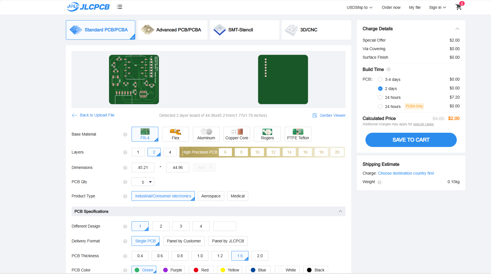
We explore JLCPCB to see how to order a board for manufacturing. The process is fairly easy just by uploading the gerber files in zip and choosing the material and PCB specification the board will be produced an ship to your location.
We have characterized two PCB milling machine for this assignment.
Roland XRM 20 (Ahmed)
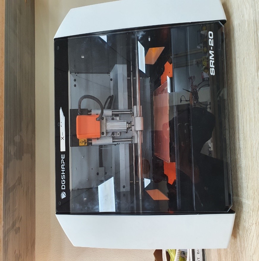
In our lab we use monoFab SRM-20 for PCB milling.
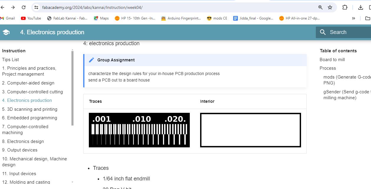
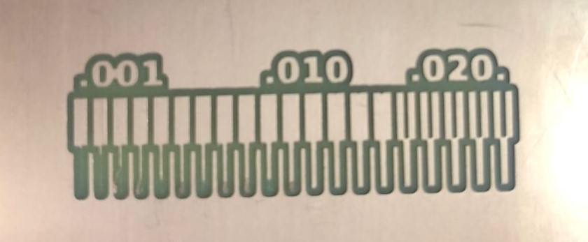
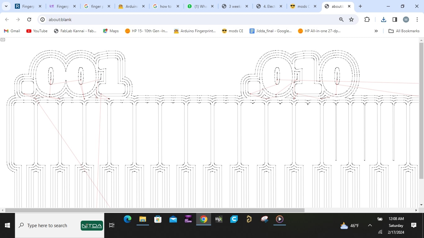
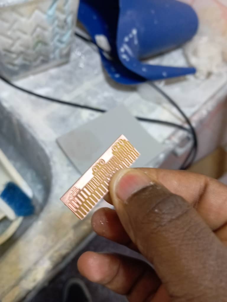
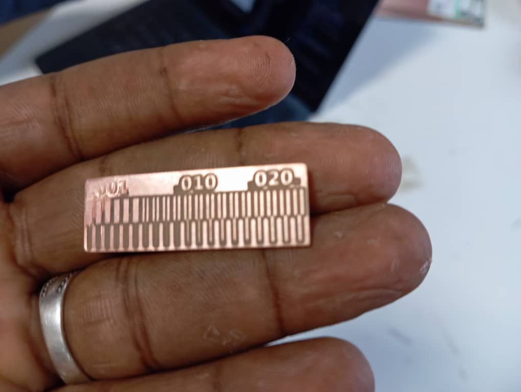
To characterize the design rules for our PCB production, we used this line test file provided to us by our instructor.
To get the desired milling file for the machine, we used modsproject.org to convert the png to RML file. We also tested milling with 2, and 1 passes as seen below:
With 1 pass
With 2 passes
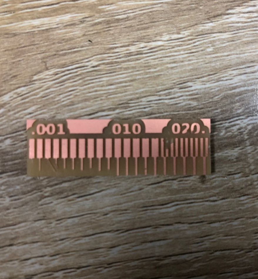
The result shows we can be able to produce board with traces separated with minimum of 0.01mm with up to 2 passes
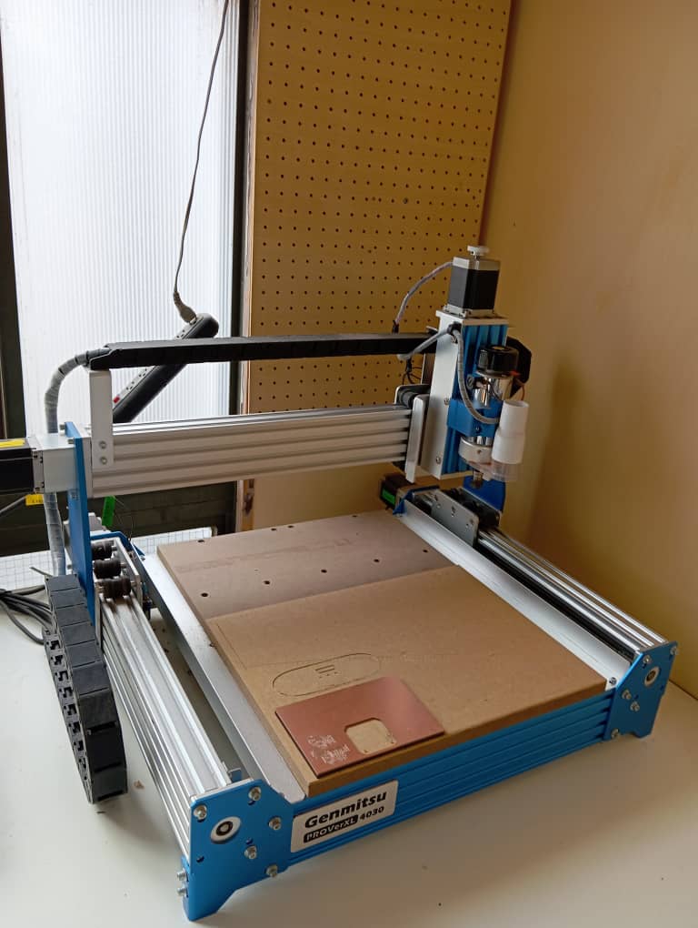
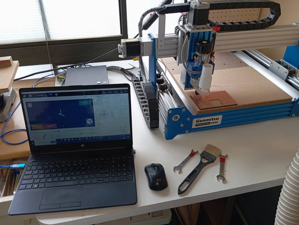
Genmitsu ProverXL 4030 (Jidda)
Electronics production is a critical aspect of modern technological advancement, serving as the backbone for the myriad devices that have become an integral part of our daily lives. From smartphones to household appliances and sophisticated industrial machinery, the seamless integration of electronic components is paramount for functionality and efficiency. The importance of electronics production extends beyond mere consumer goods, influencing sectors such as healthcare, communication, transportation, and beyond. (chat_gpt).
Electronics production is therefore one of the key skills being taught on fabacademy Courses. There are several techniques used in electronic PCB production and for this weeks session we are working on the milling technique.
Activity
This week group task is to characterize the design rules for PCB production process and send a PCB out to a board house.
The activity is thereby divided into the following 1. Preparation of Milling DATA 2. Machine operation (milling) 3. Observation and post milling Processing
Preparation of Milling Data
To obtain and prepare our milling data we follow the following processes:
-
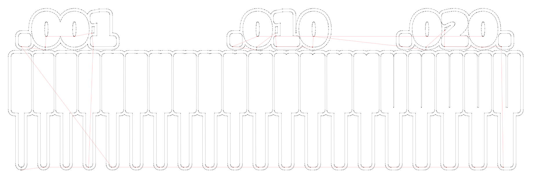
We downloaded the linetest_trace and linetest_interrior files from our local instructor web page


-
After Obtaining the already design, we then used Mod Site to generate our gcode. MOD is used to generate gcodes to be used for milling by multiple milling machines.
-
we started by loading the mod site
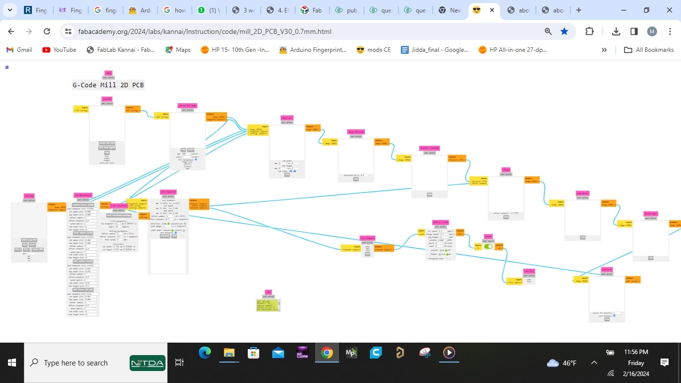
-
then we imported the downloaded png images by clicking “Select png file”. we started with trace because the interior will cut the board out.

-
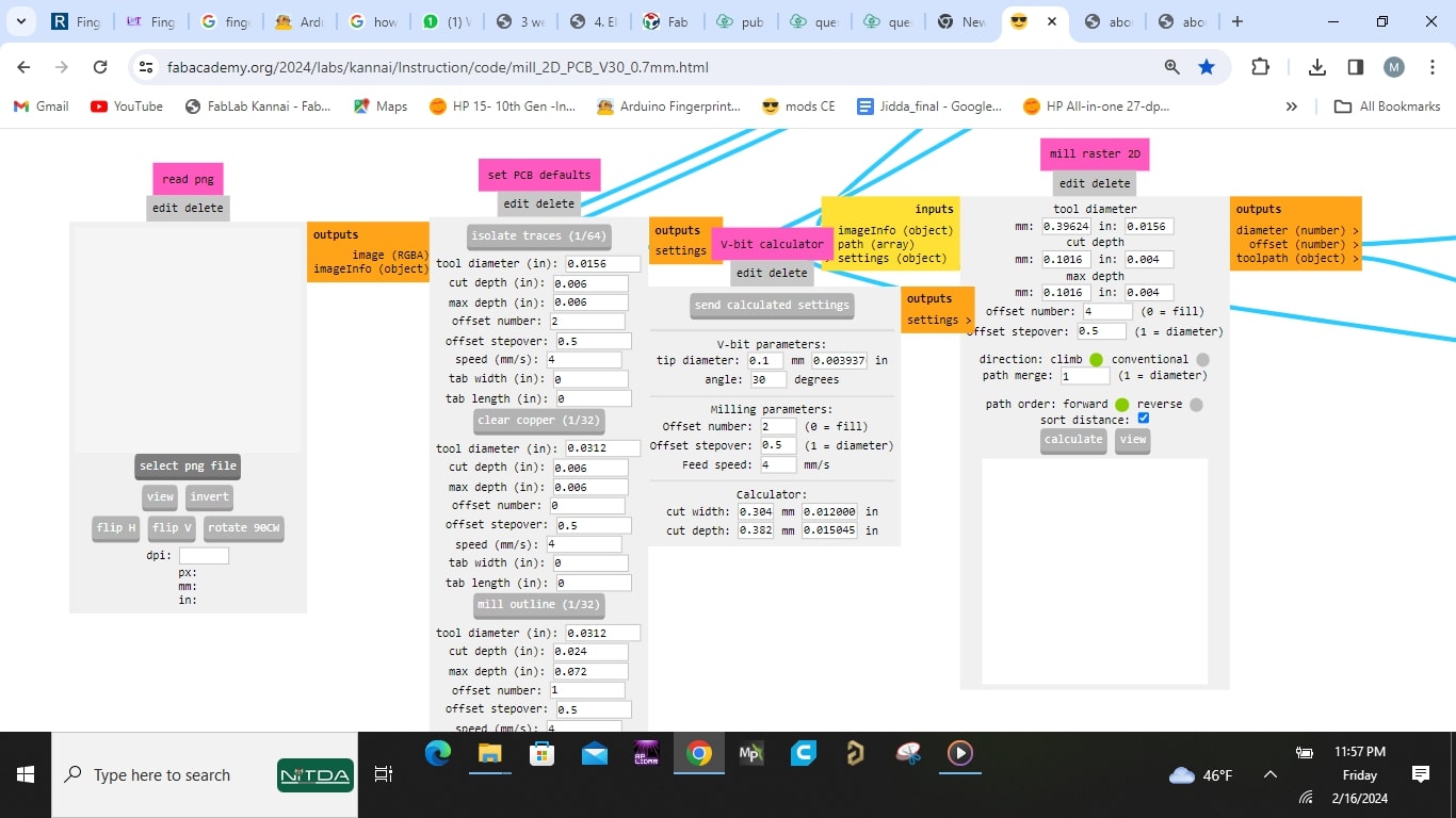
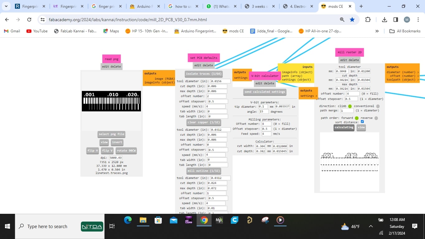
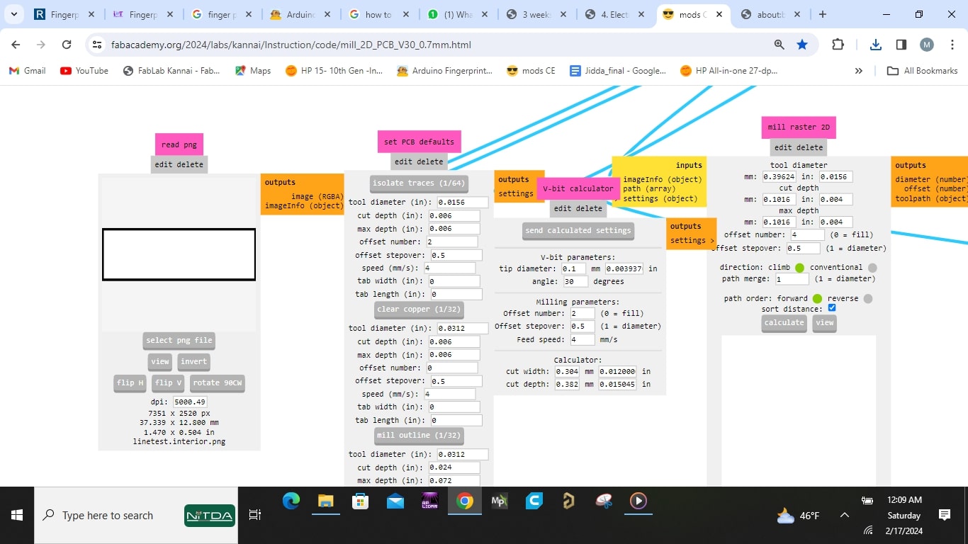
Since this is trace, we chose vbit calculator and inserted the values for our vbit:
- tip diameter = 0.1mm
- degree = 15
- offset= 4
and then clicked send calculator setting.

-
The cutting flow now appeared in the display section under mill raster 2d as seen in the image above , we then confirmed the data in its section and made sure its what we sent above, then we clicked calculate.
Immediately a file was downloaded containing the gcode titled linetest_trace.nc and a view was displayed. sometimes one has to click the view button beside calculate to see the view.
-
we then repeated similar step of import png file into mod for the Interior file.
-
As explained earlier, for interior outline milling we use the o.7mm flat end mill, so we go under “set pcb defaults” heading and used the section set “mill outline (1/32)” with the following values:
- tool diameter = 0.02755 in (0.7mm)
- cut depth = 0.02755 in (0.7mm)
- max depth = 0.06692in (1.7mm)
- offset number = 1
- tab width and length = 0
- speed = 4
and then clicked the section header (button) “mill outline (1/32)”.
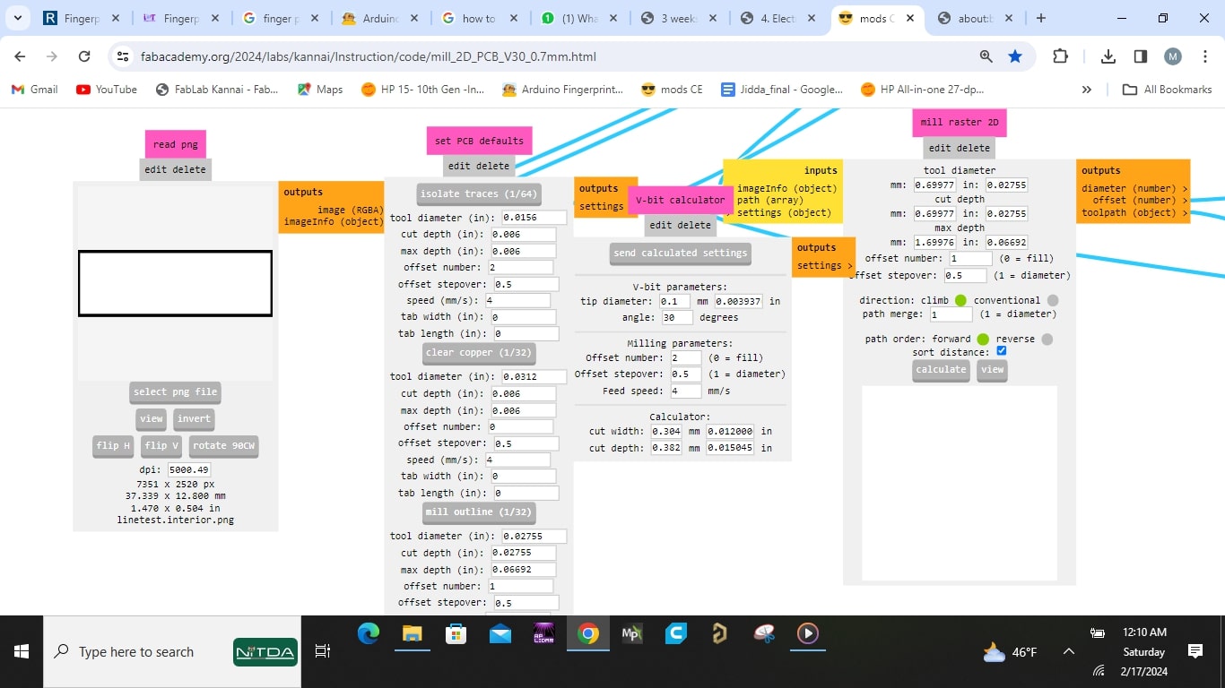
-
After that the interior flow appeared under the display section under mill raster 2d, we then confirmed the data in its section and made sure its what we sent above, then we clicked calculate.
Immediately a file was downloaded containing the gcode titled quentorres_trace.nc and a view was displayed for me. sometimes one has to click the view button beside calculate to see the view.
-
Then our data is complete and we head to the maching for milling .
Machine operation (milling)
We were introduced to safety aspects of using milling machines first as a measure to prevent accidents and inefficiency. Some of the safety precautions are as follows. - One has to be with the machine while in usage - The machine surface and bed must be thoroughly cleaned using the vacumm pump before and after usage - The milling bits are very fragile, one has to be extra careful when changing or handling them - the spindle is fast and the bits are sharp, one has to stay clear from the working area of the machine when machine is milling.
We used Gsender application as the interface to load Gcode to the machine as well as control the machine. After That we then:
- Placed our work piece on the table, using double sided sticky tape to hold it firm and prevent it From moving while milling takes place
- switched on the machine and connected laptop to it
- launched the Gsender file and uploaded the Already Generated linetest_trace Gcode which we gor from mod.
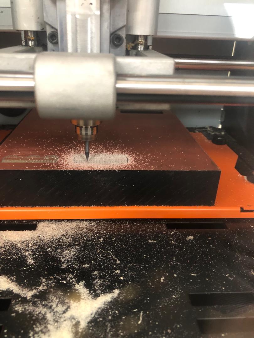
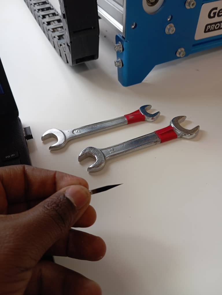
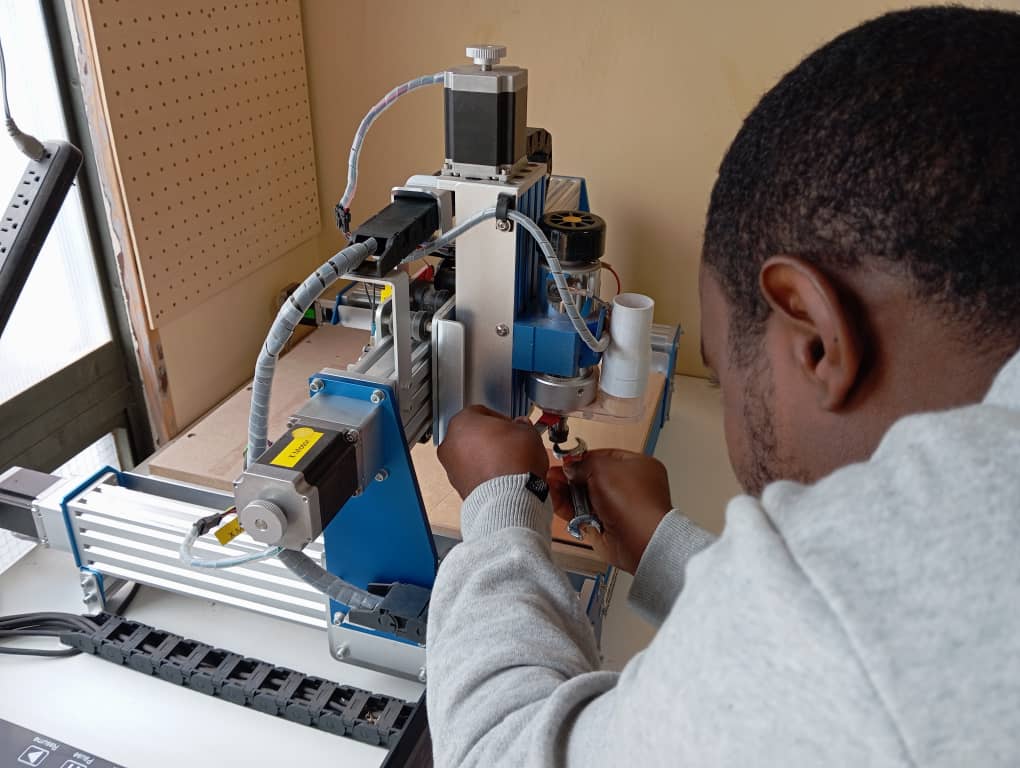
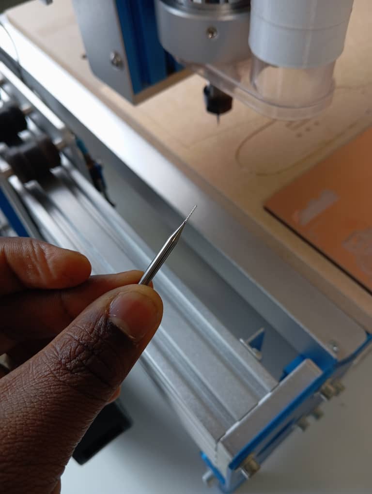
- used the x,y and z axis control on the software to come to the front access area and then inserted Our Milling bit. We used The Vbit 15 degree tip diameter = 0.1mm
- used the x,y and z axis control on the software to set our x and y zero.
-
then placed a paper and manually set our z zero by bringing the tip of our bit onto the paper surface until a grip is felt.
-
We then start the milling.
-
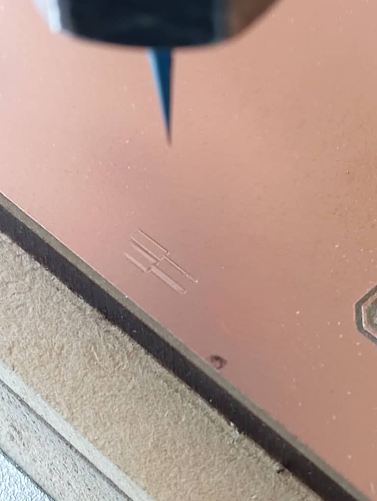
Just as milling started we noticed that the tip of our bit got broken and it was not cutting deep enough.
-
so we had to change the bit and the we use the 30 degree vbit.
-
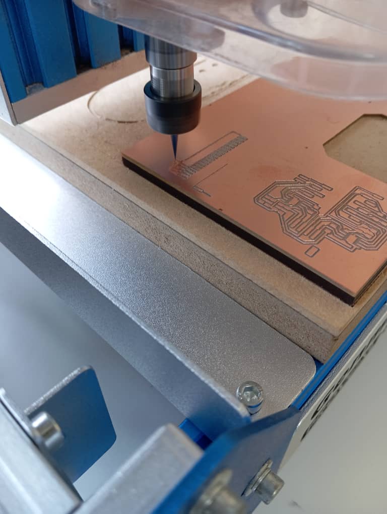
The trace was then completed and we change the bit to flat end mill for cutting the board out.
-
Then we run the interior gcode file we generated from mod and the milling process is completed.
Observation and post milling Processing
After milling the board we
-
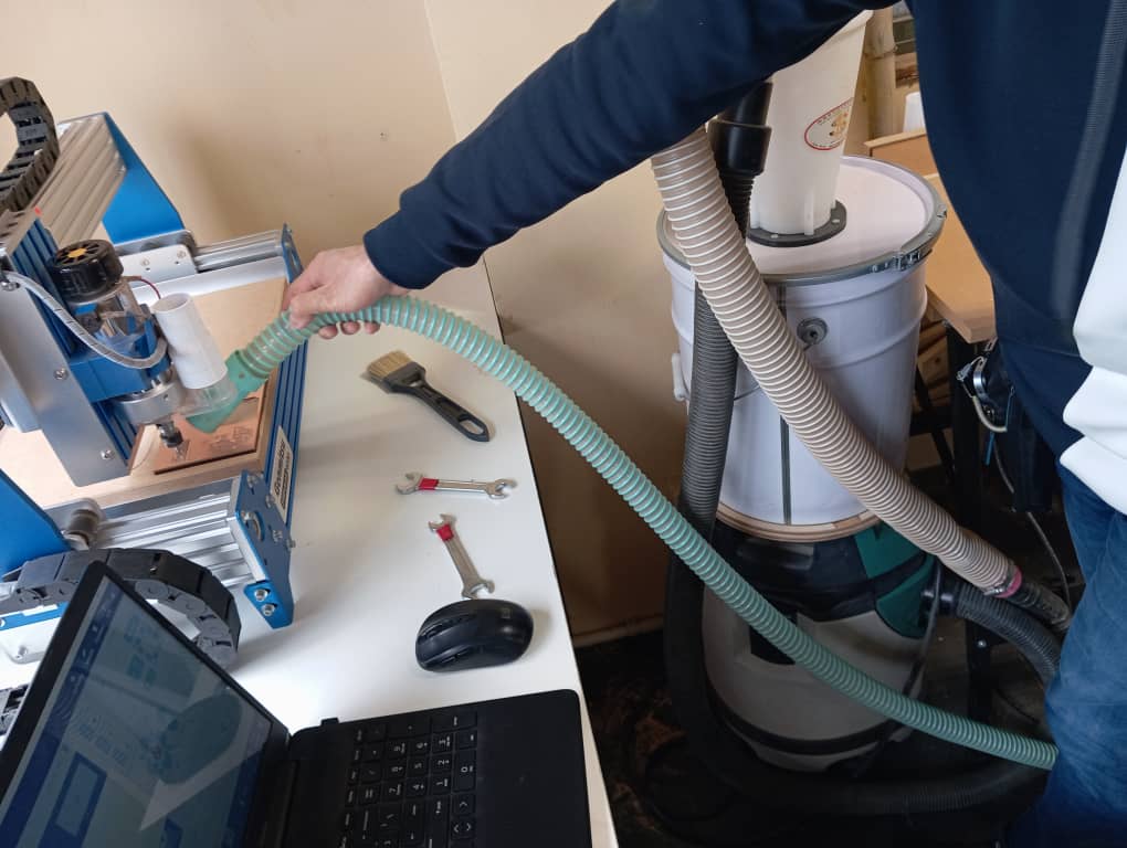
used the vacuume pump to suck away the dust particles on the machine
-
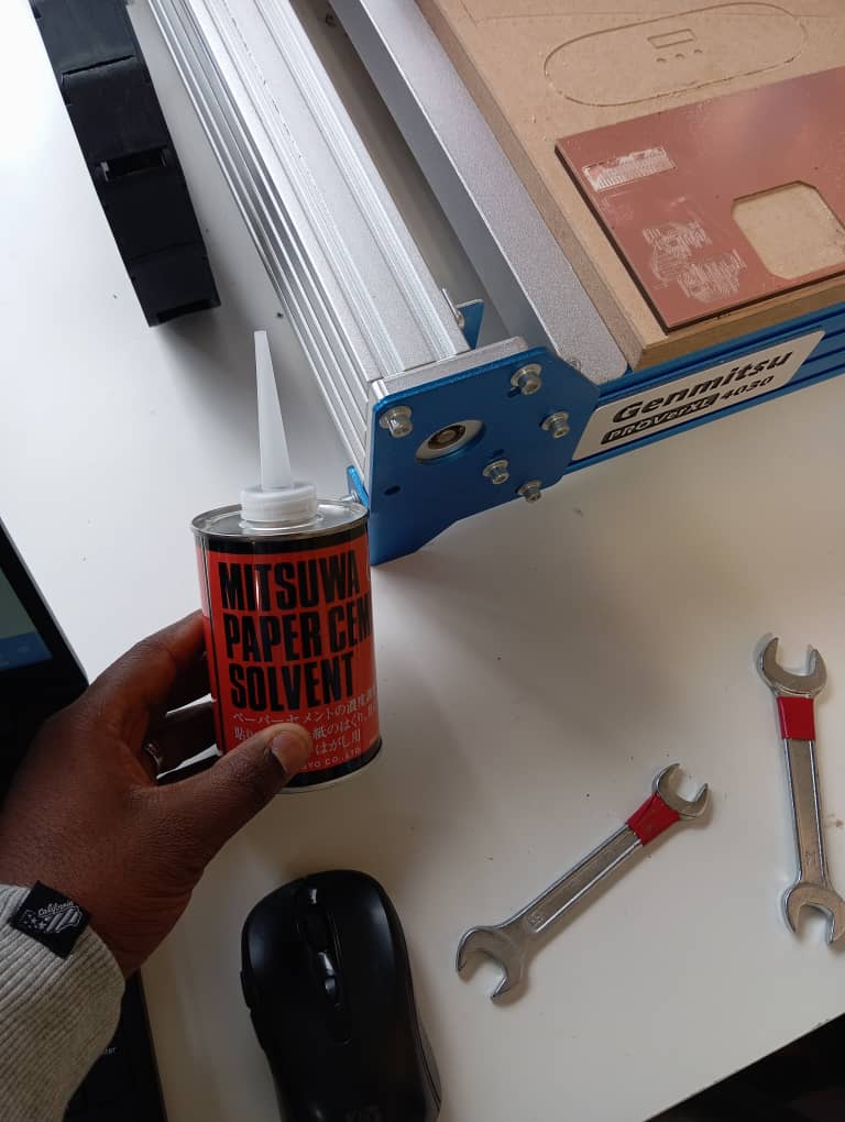
applied paper solvent to weaken the adhesiveness of sticky tape used in keeping the board in place.
-
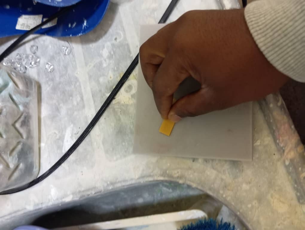
gently brushed the surface of our board with fine grain sand paper.
-
then use liquid soap to wash the surface
Observation
We observe the following: 1. That Vbit 30 degree is stronger and more reliable than 15 degree 2. If succeeful, Vbit 15 degree gives better routing as it takes less width of copper as compared to 3o degree 3. The un-flatness of bed or the variation in thickness of the pcb workpiece can have effect on the output, as seen the vbit did not route the top left corner of our board because there is a little variation in board thickness.
With this we come to the end of our documentation.