Week 11 - Input Devices

Assignments | Week 11 | Input Devices
Group assignment
Probe an input device(s)’s analog and digital signals Document your work on the group work page and reflect on your individual page what you learned
Individual assignment
Measure something: add a sensor to a microcontroller board that you have designed and read it.
Learning outcomes
Demonstrate workflows used in sensing something with input device(s) and MCU board
- Week 11 - Input Devices
- Introduction
- I - Design and fabrication process
- II - The programming process/es I used
- III - The 2 Problems I encountered and how I fixed them.
- IV - Original design files and source code
- V - Hero Shot of the board
- VI - What did I learned from Group assignment
- Conclusion
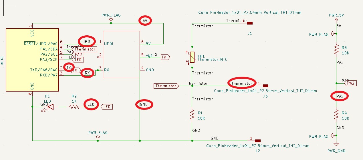
Introduction
This week, we are going to
- Analize how captors or sensors works, by transmit analog signals
- How the signals are interpreted by the mcu,
- Understand the mechanism and logic of an input devices
- The complementary role it plays with output devices.
- Also, how input devices are beneficial.
I - Design and fabrication process
1. Picking the input device: Thermistors
We have a large range of input devices that we can choose to manipulate for this week
- switch
- magnetic field
- potentiometer
- step response
- temperature
- light
- motion
- distance
- location, time
- acceleration, orientation rotation
- sound
- vibration
- force
- angle
- pressure
- pulse
- air pollution
- gases
- image
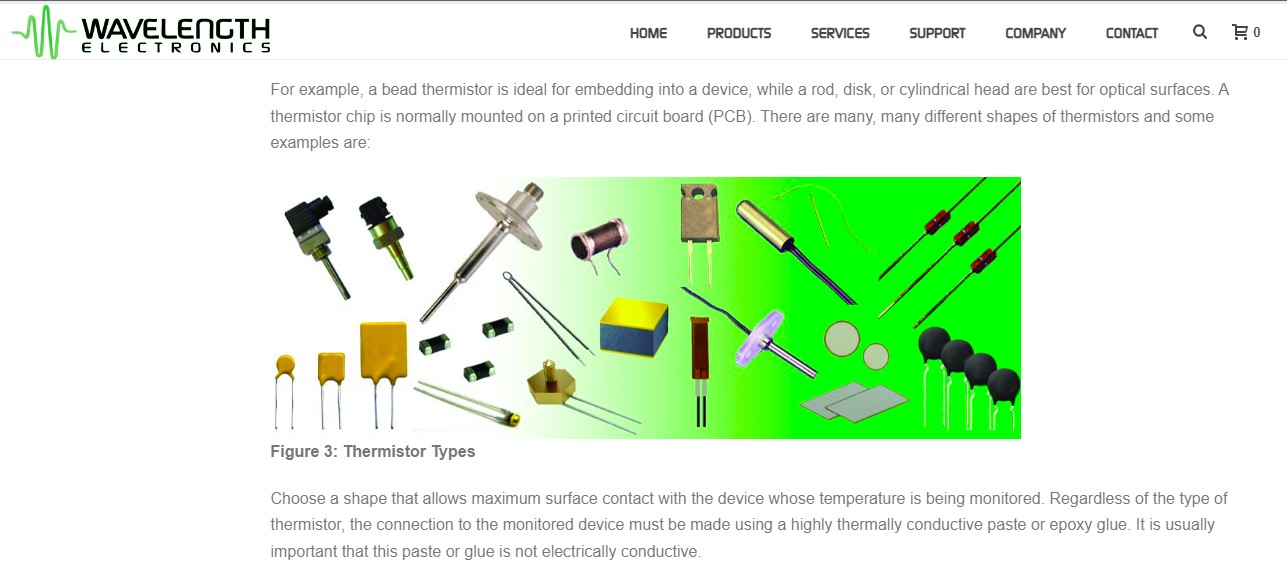
Thermistor
I choose the thermistor as the input device of this week. The demonstration video of the thermistor that Neil show us was the most easy to understand for me.

I did a brainstorming to visualize the real-life application of thermistor.
What is a thermistor? I imagine that it is a temperature sensor that receive heat and tranform the heat to analog signals… Maybe it’s not right, I’ll check this information later. A commun example for temperature sensor is Thermometer. Oh, we also can find temperature sensor in objects or machine where we need to control the temperature, like computer, smartphone, refrigerators, air conditioners, and water heaters… It’s so fascinating to find out that this little sensor is surrounding us in some way. But, I still don’t know what is a thermistor. Is it similar to a thermometer? The picture that Neil shows us seems like a resistor. A thermometer+resistor? What’s the point, and why it has been invented as an input devices for pcb?
Research and Answers

What is a Thermistor?
Before reseach
A temperature sensor that receive heat and tranform the heat to analog signals
After reseach
A resistor that changes its value in function of the temperature. In other words, the resistance of this component changes with temperature.
Is it similar to a thermometer?
Before reseach
A temperature sensor that receive heat and tranform the heat to analog signals
After reseach
A resistor that changes its value in function of the temperature. In other words, the resistance of this component changes with temperature.
why it has been invented as an input devices for pcb?
I don’t know
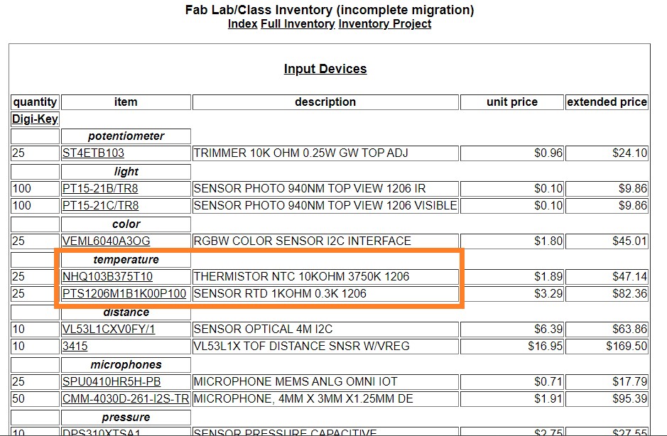
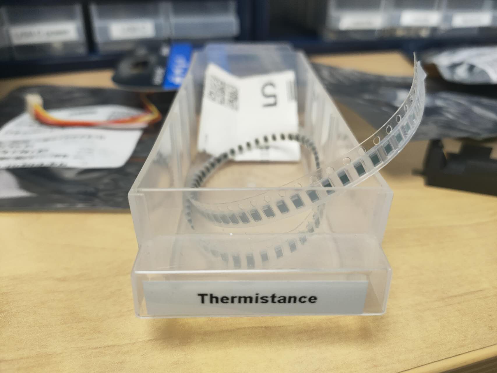
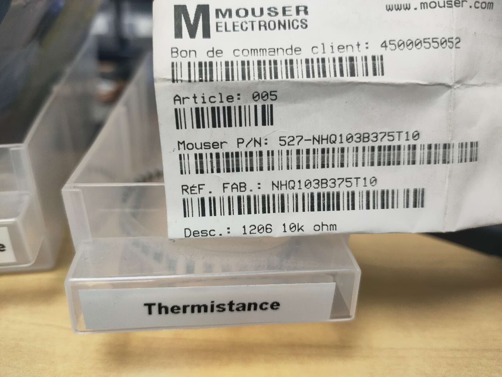
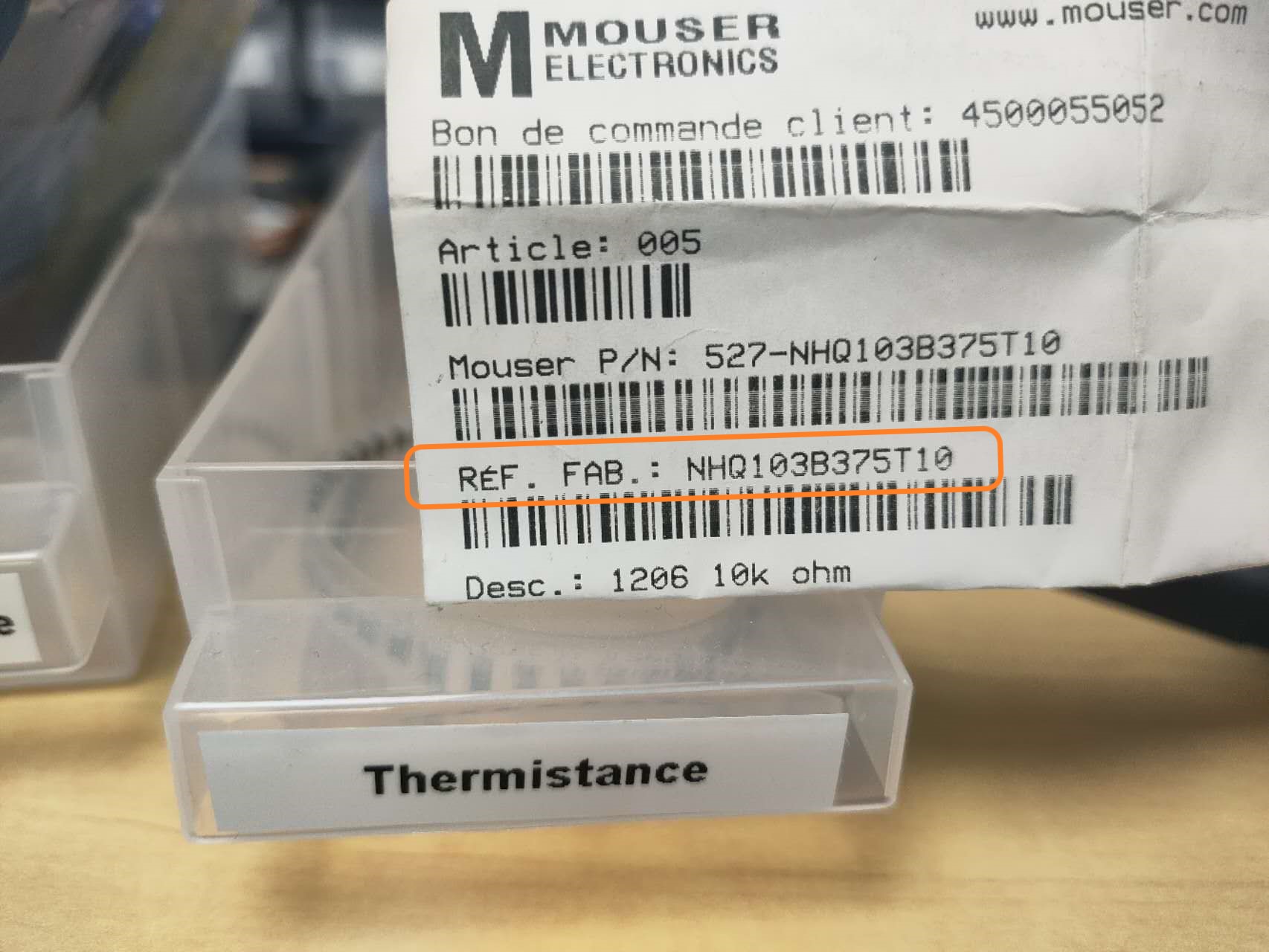
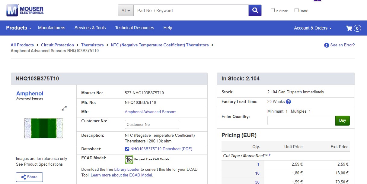
I checked the electronic component’s stock of thermistor
Searched the reference NHQ103B375T10 on the web and found it.
2. Designing the PCB with Thermistor: KICAD
2.1 New project and components
I created a new project and added components:
| Component | Quantity | Schematic | Footprint |
|---|---|---|---|
| thermistor | 1 | termistor_schematic.jpg | |
| attiny 412 | 1 | at412_schematic.jpg | |
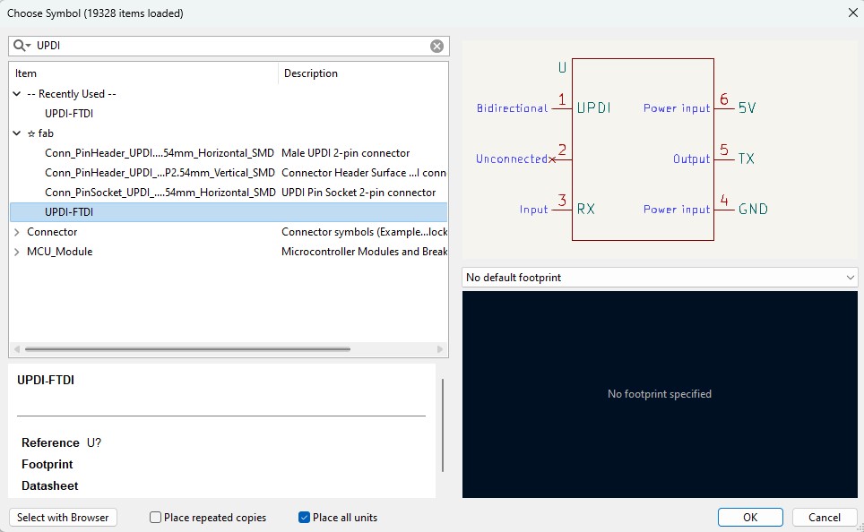
| UPDI-FTDI | 1 | updi_ftdi_schematic.jpg | |
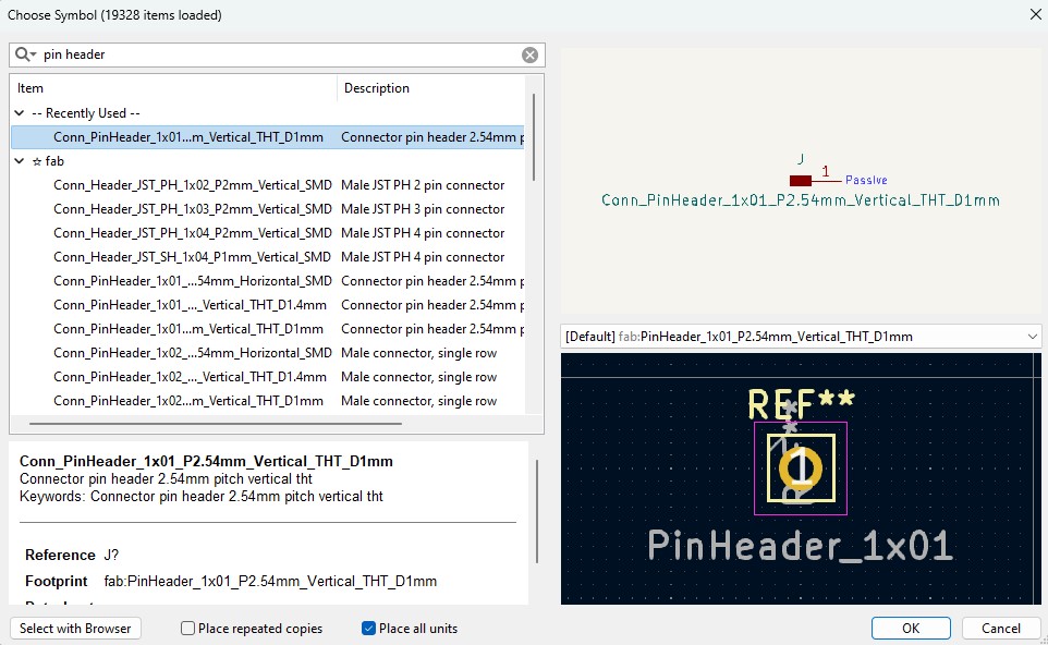
| 1 pin vertical header | 3 | 1pin_schematic.jpg | |
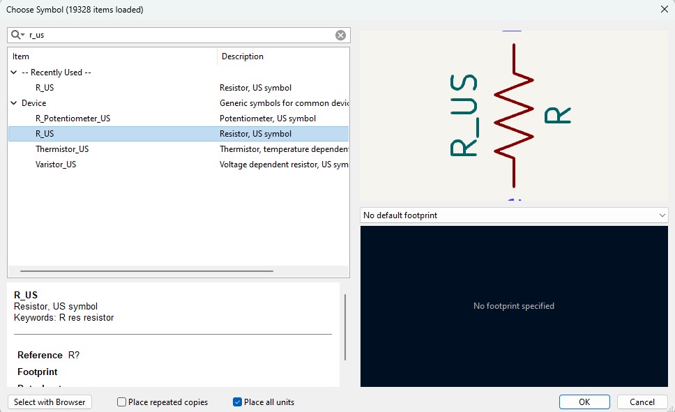
| 1K resistor | 1 | r_schematic.jpg | |
| 10K resistor | 3 | r_schematic.jpg | |
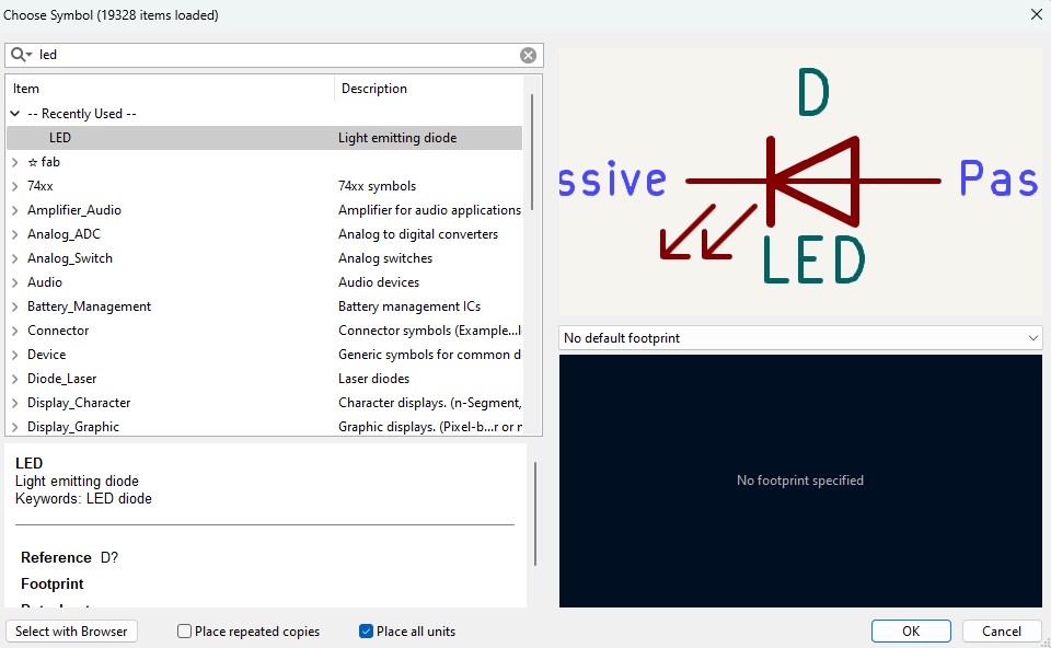
| LED | 1 | led_schematic.jpg |
The first version of the schematic
Stephane recommand me a template to follow. The idea was making a pcb that allow us to analyze the signals of the thermistor by climping the multimeter or the oscilloscope on the vertical pin.

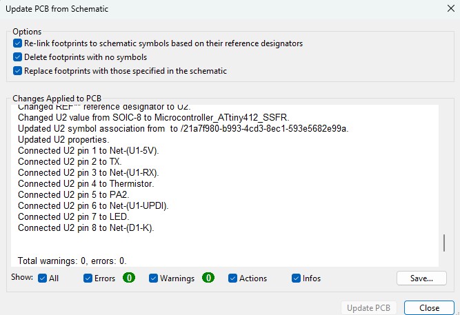
During the designing process I modified the first version after an ERC (Electrical Rules Check). You can check it out by clicking on this link to the title Problem 1. Kicad Electrical Rules Check (ERC) or just keep reading.
Problem 1. Kicad Electrical Rules Check (ERC)
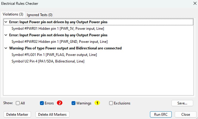
When I ran the ERC, I have a warning message and 2 errors.

I selected the warning issue and see that the pointer points the power flag.
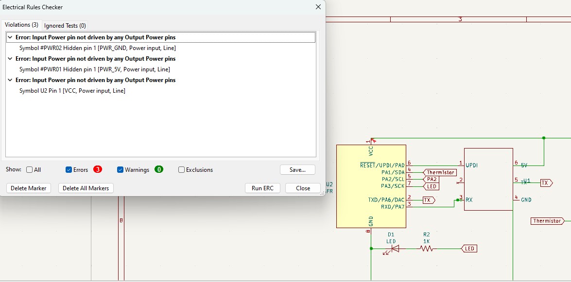
I deleted it and got another error instead of warning. Then I realized that the problem isn’t this power flag but something else.

I deleded the link between the pin header and 5V because the power of the pin header normally comes from the global label “Thermistor” which is connected to the vcc of the microcontroller. I also added two power flag to tell the ERC where the power comes from.
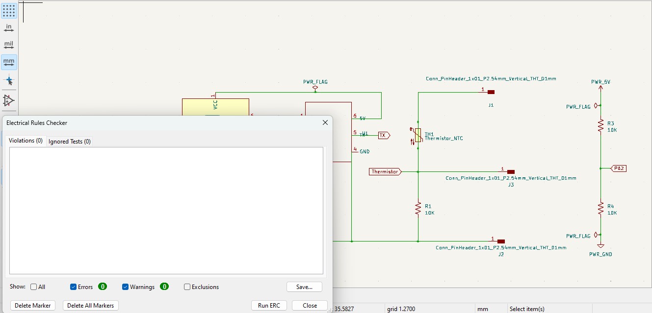
Now I have no warning neither error.
But this problem resolving created another problem…
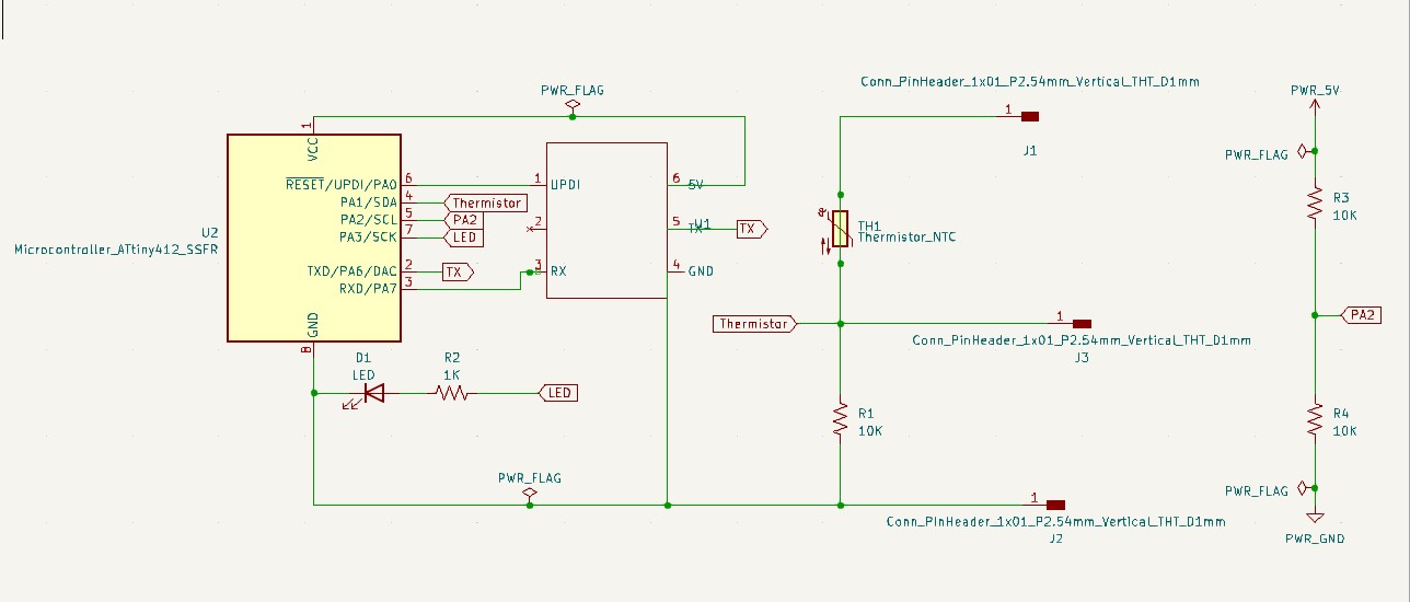
The final version of the schematic
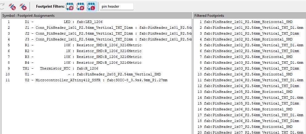
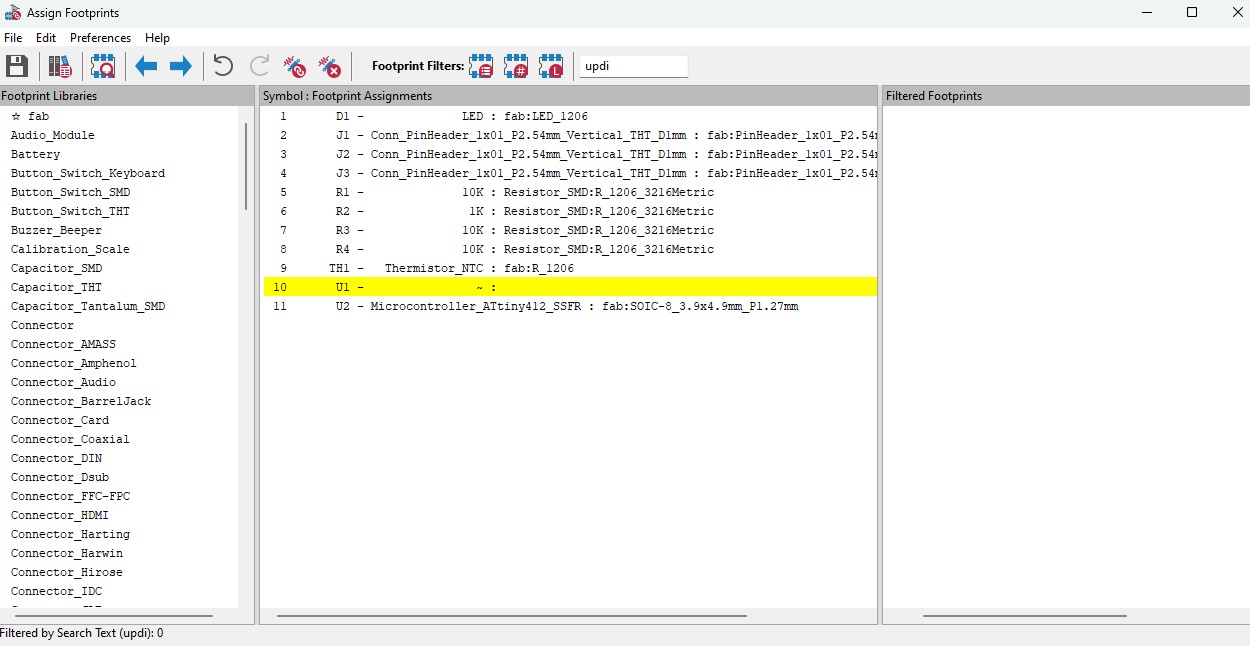
2.2 Footprints assignments
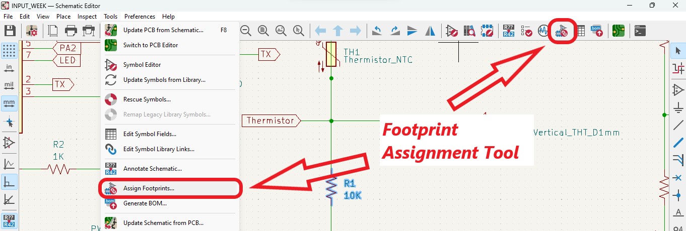
Open the footprint assignment tool.

Assign to each component a footprint that correspond to the component that you’re going to use.
Footprints assigned
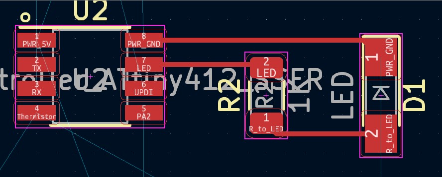
2.3 PCB Editor
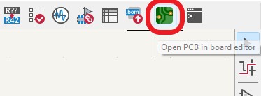
Open the PCB editor
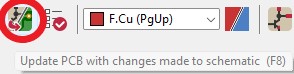
Update the components’s footprint in the PCB Editor.
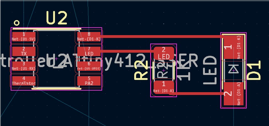
Rename the nets for clarity

Add net label
All nets are named.
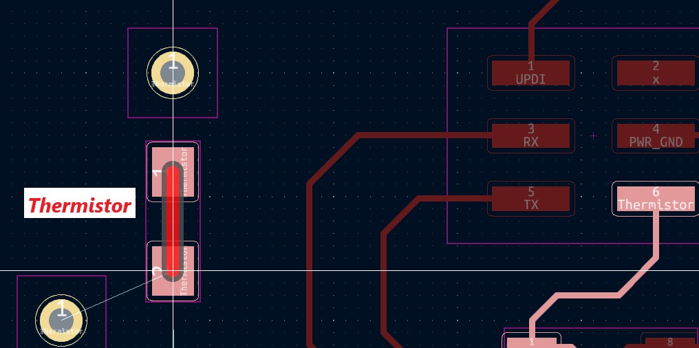
But, this decision engendered a problem for the pcb tracing: The two terminals of the thermistor were connectable, even though they were not supposed to be linked 😢
After checking with instructor Stephane, we only kept a few net label. Because the nets connected to a global label are already named by the global label! So it is unnecessary to name a net already named 😉
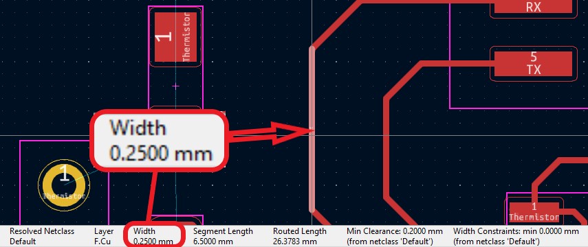
He also point out that the traces on my pcb board are too thin: 0.25 mm . I have to change the settings to 0.4 mm or 0.5 mm. It will be easier to make with cnc machine. because we don’t have end mills with 0.25mm of diameter. The thinest we have is 0.3mm..? (à vérifier)
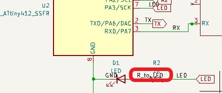
Added R to LED net and !
PCB Design Rules Check

The design rules checker indicates that the edge cuts graphics were aligned between them.
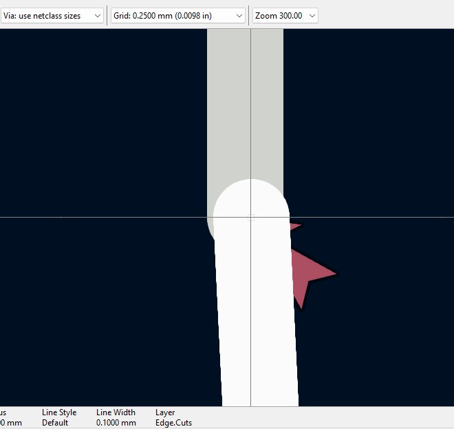
The problem became clear when I zoom into the zone where the issue marker is. The line was not aligned with the arc.
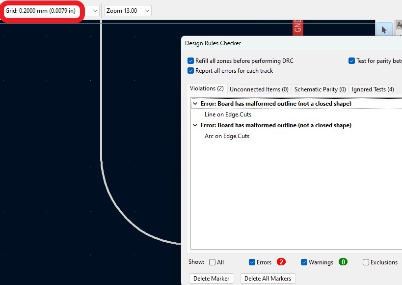
In order to move the graphics more precisely, I adjusted the grid scale from 2.5mm to 2.0mm.
I finally deleted all and start from zero.

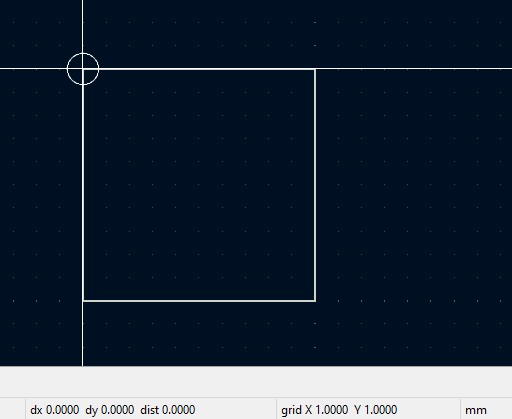
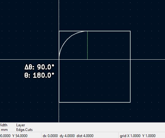
by aligning the rectangle’s start point at a unit and using 1mm grid I was able to create the edge cuts layer with no error.

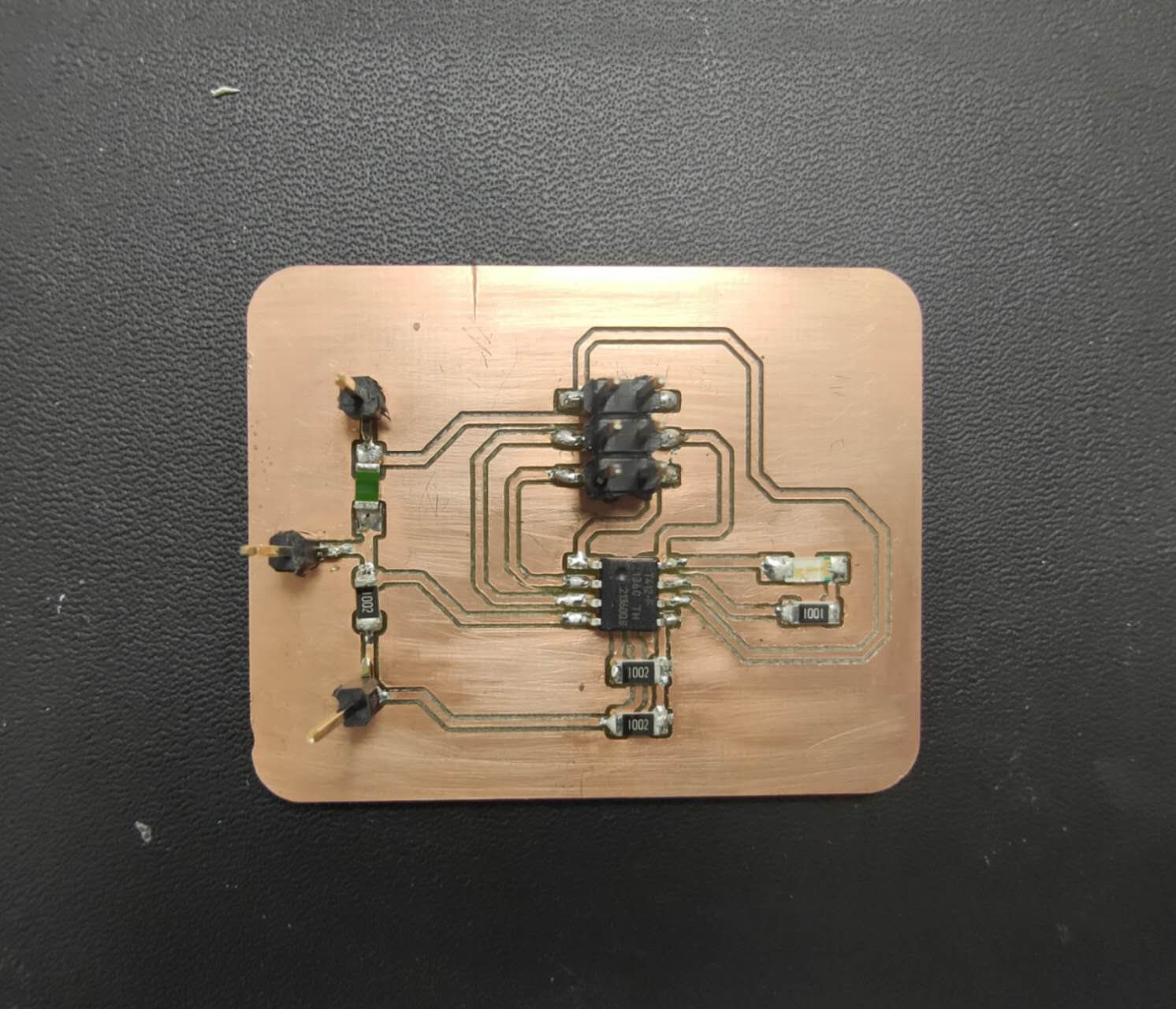
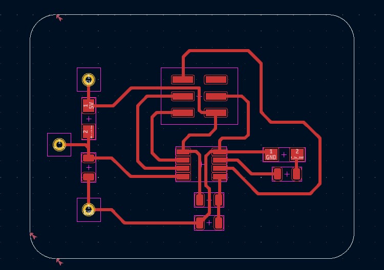
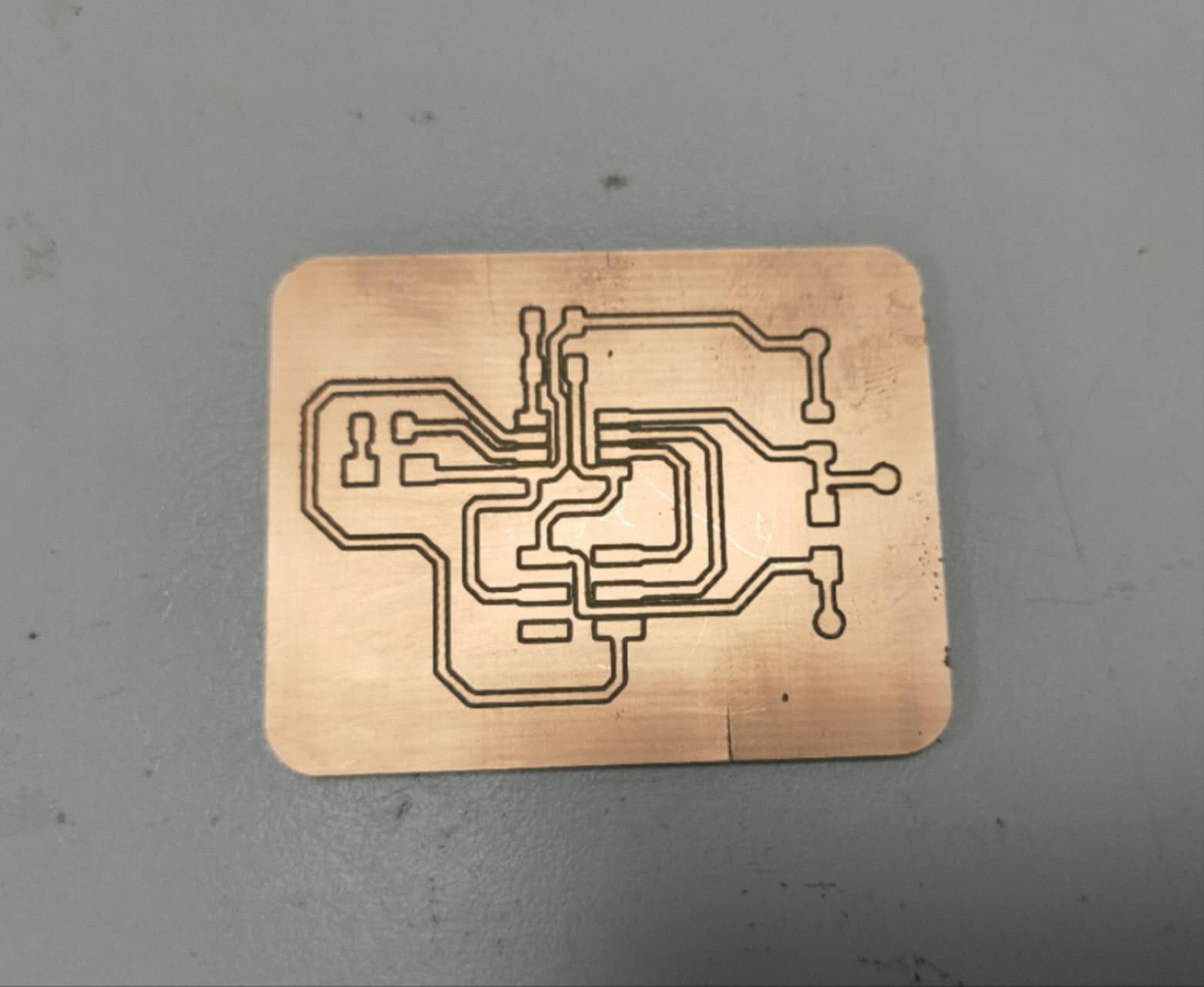
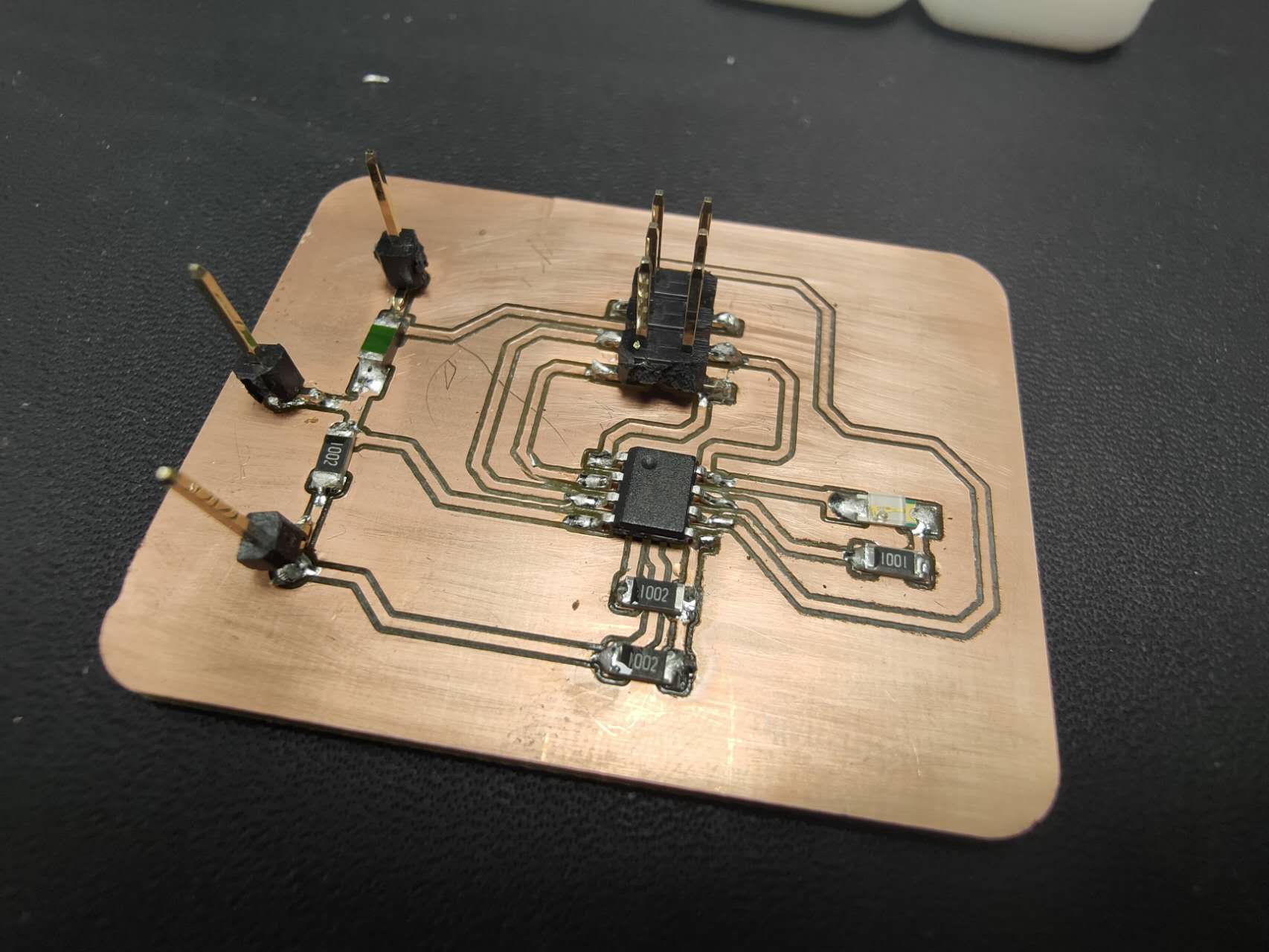
Final version of my PCB
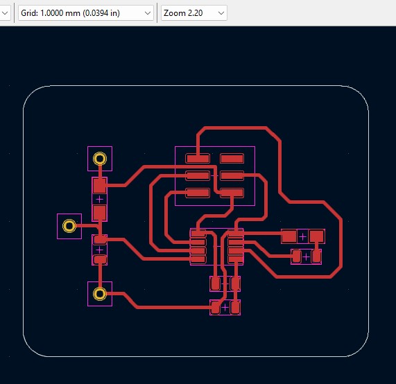
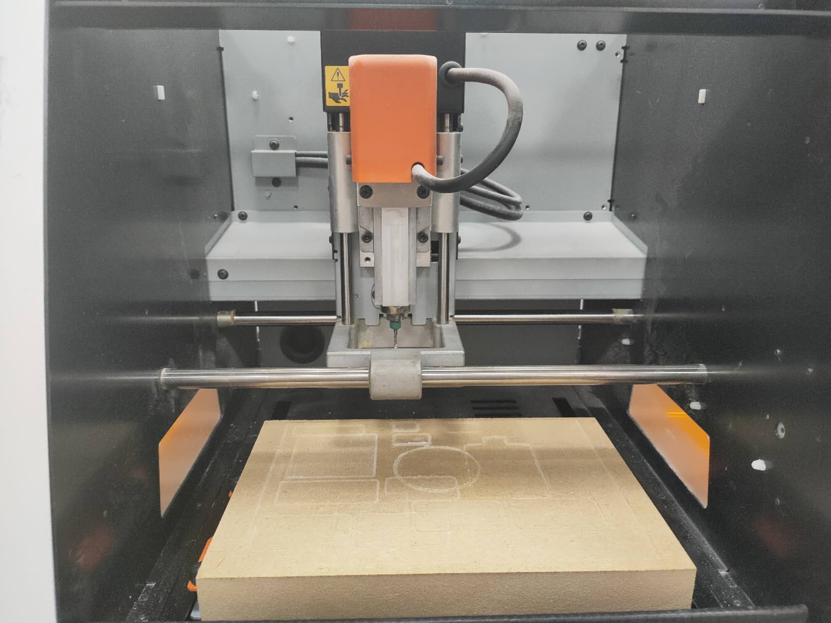
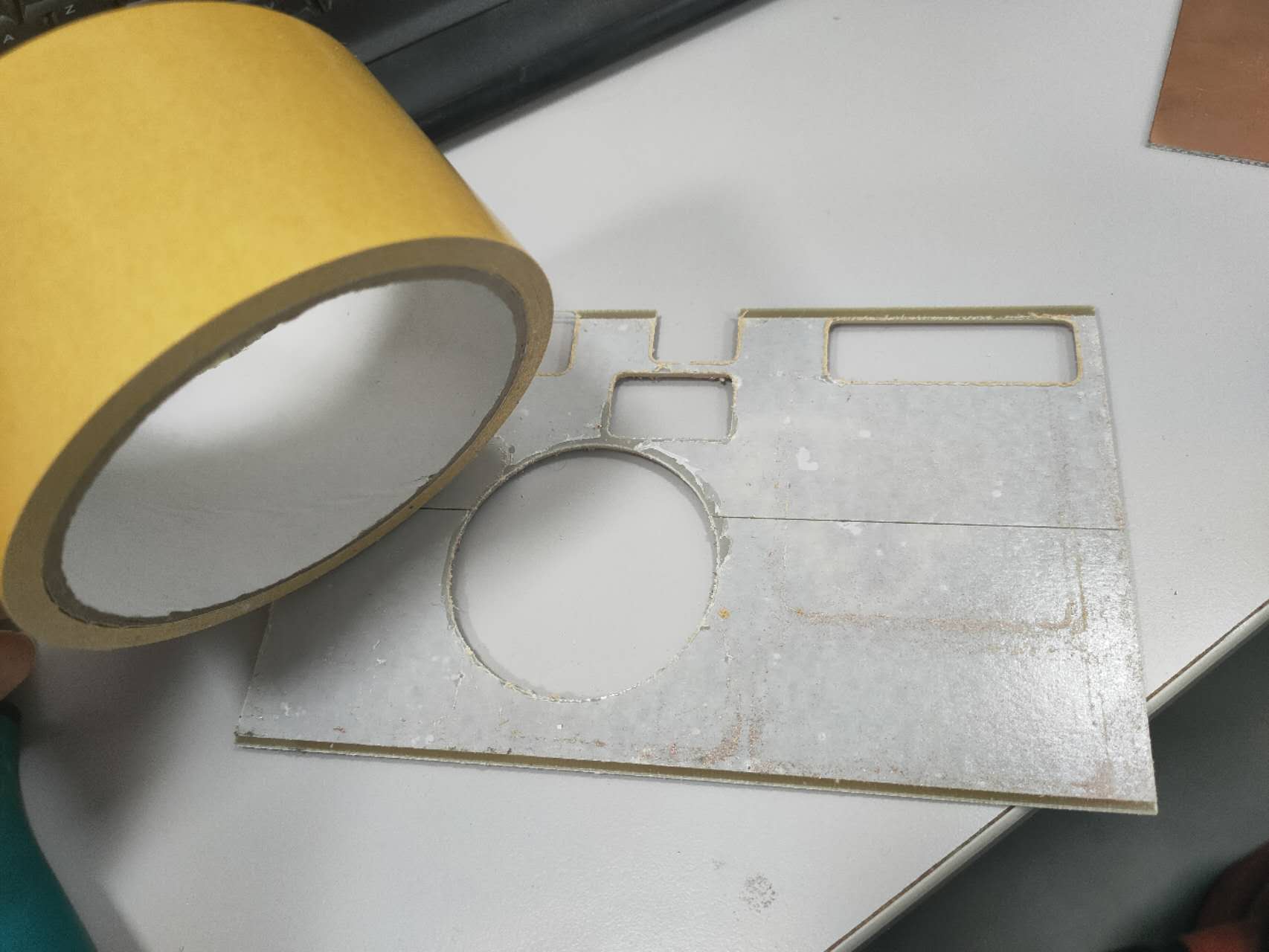
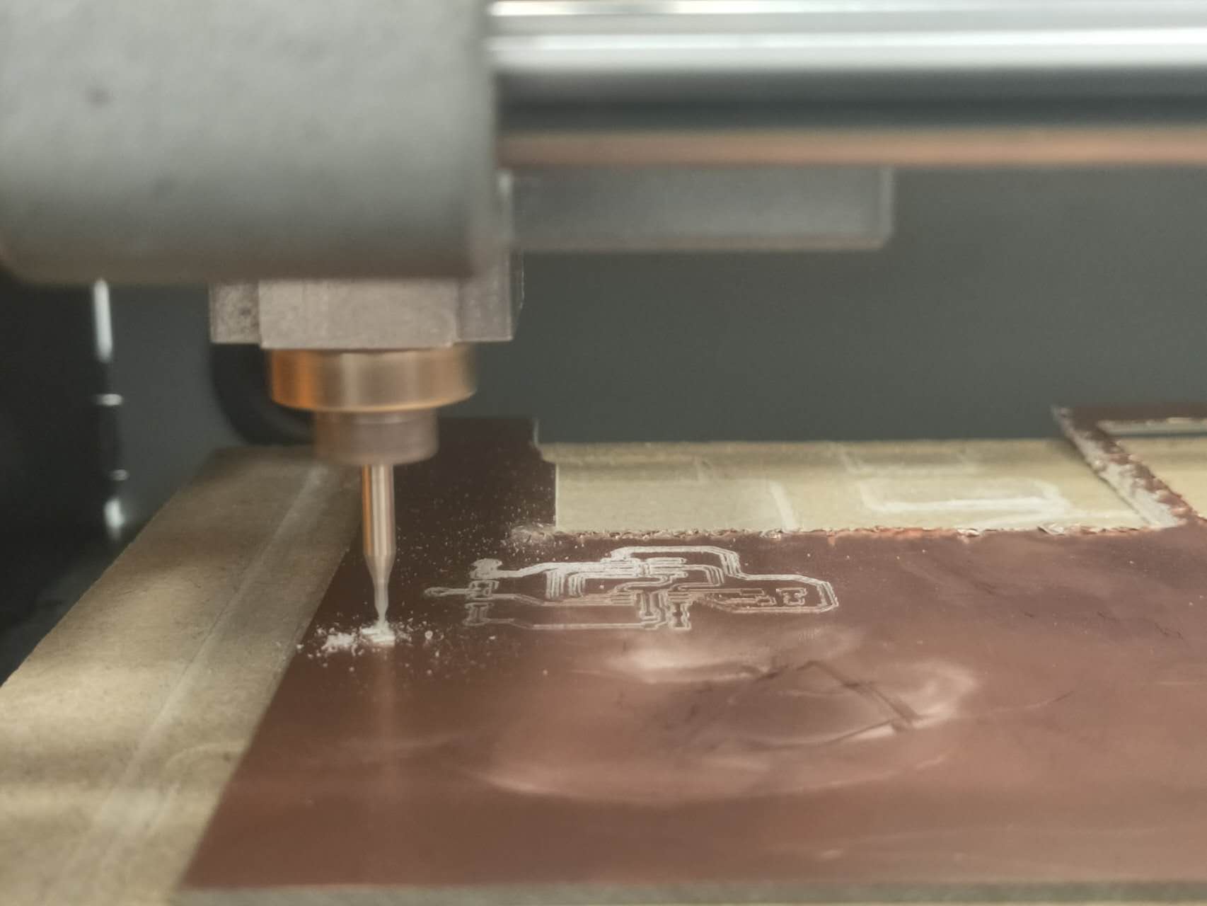
3. Making the PCB: CNC production
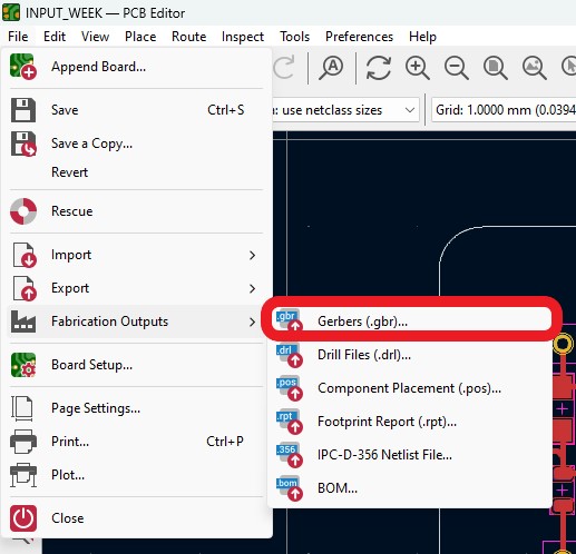
Export the gerber files
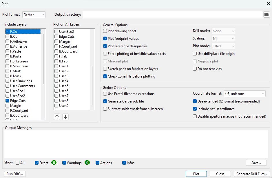
Select elements to plot
In FlatCAM:
File > Open > Open Gerber > Select the gbr files
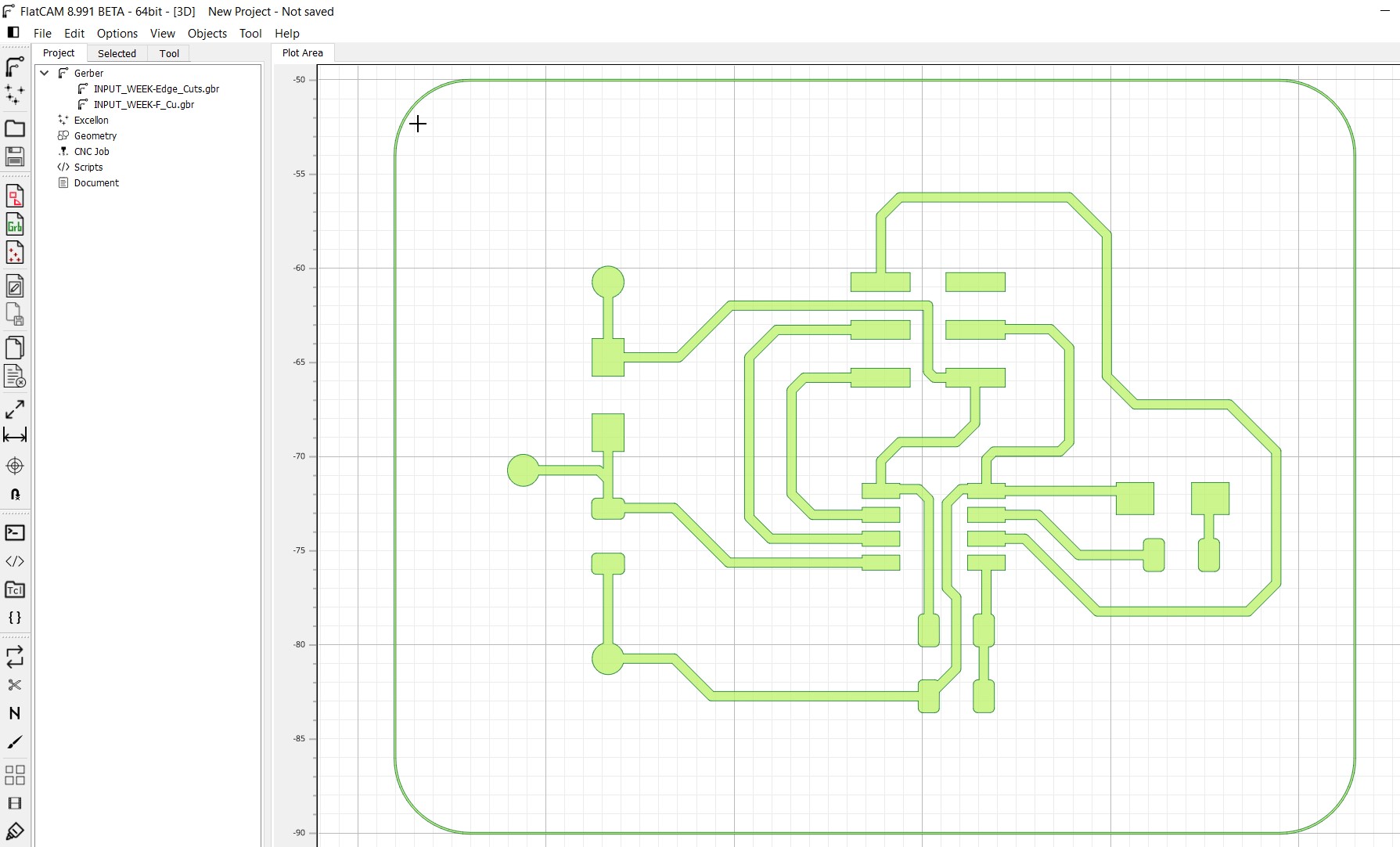
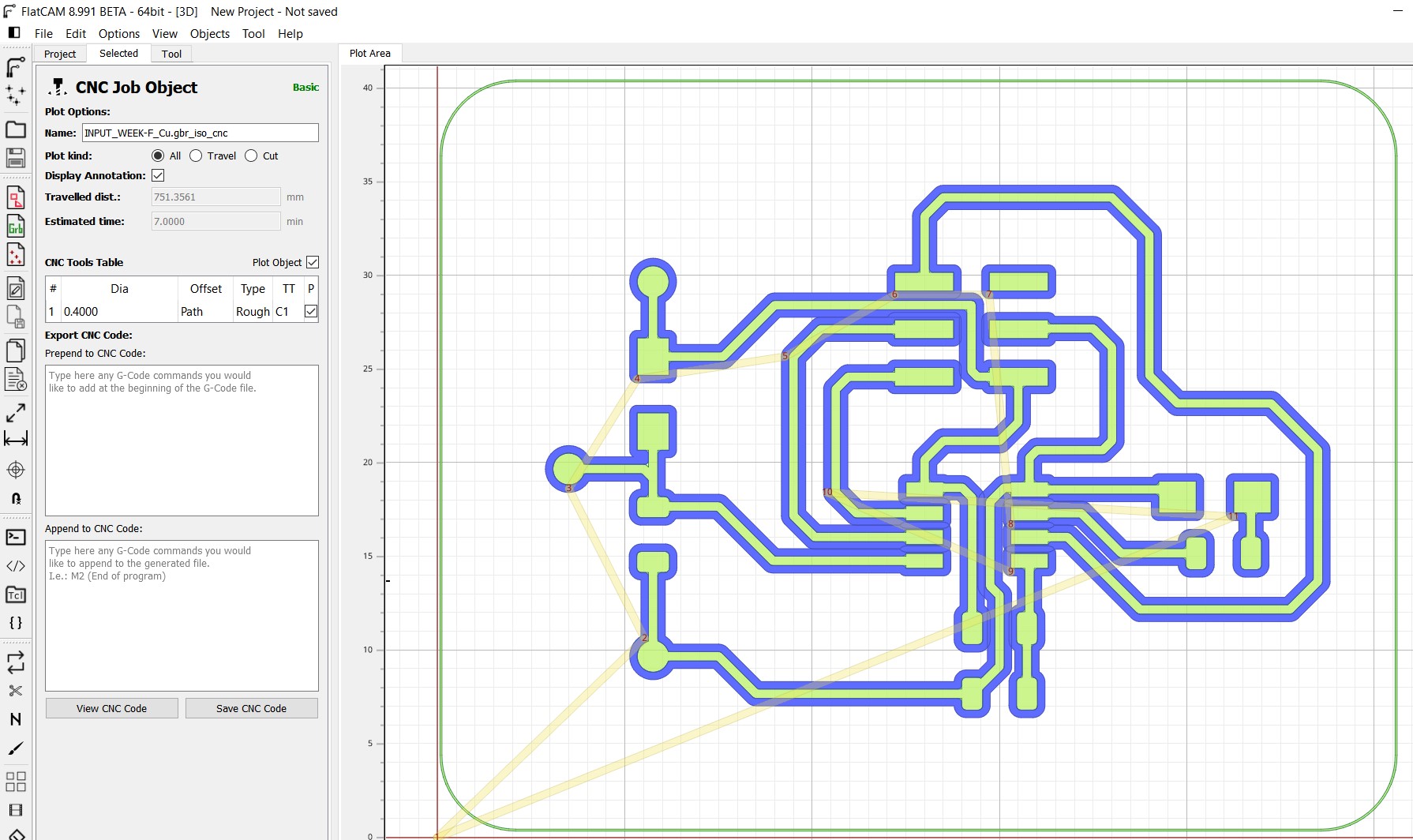
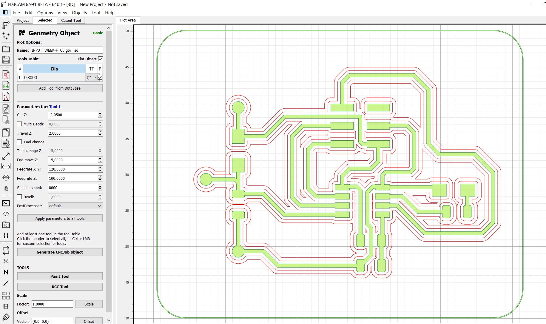

The cnc machining process.
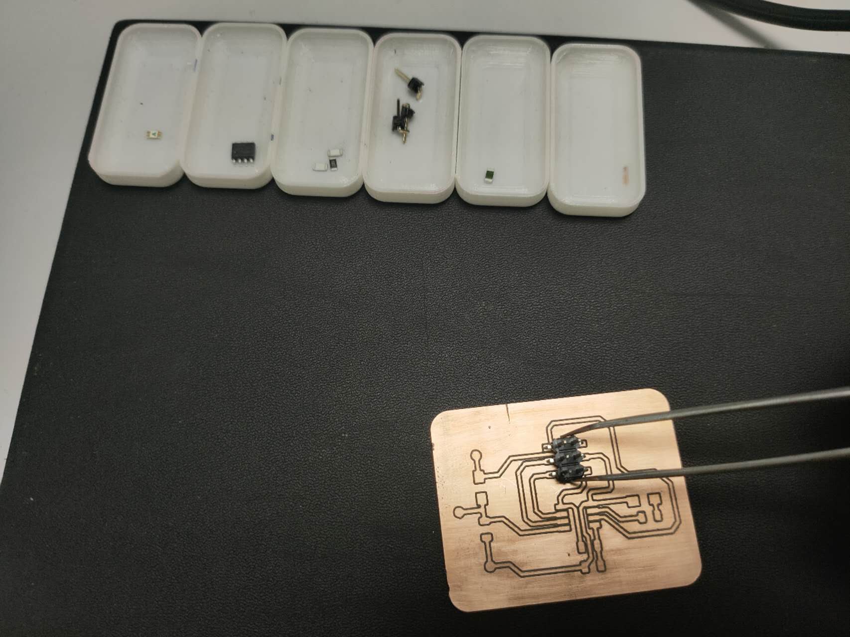
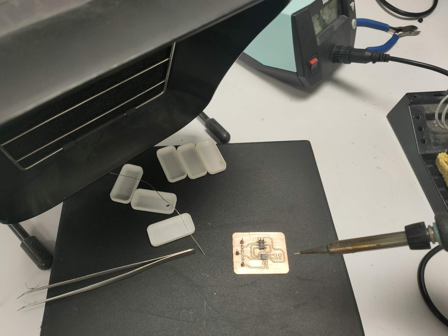
4. Soldering the components
I discovered the
II - The programming process/es I used
1. I2C communication protocol
III - The 2 Problems I encountered and how I fixed them.
2. Footprint Assignment: no footprint on library
Go back to footprint assignment
I couldn’t find the footprint of UPDI-FTDI!
I opened the footprint library to see if the fab’academy’s footprint library is missing. Answer is it is not missing.
All of a sudden, I remembered something that I had forgotten. In electronic design week, I used the same component to create my first development board!
So I opened the first kicad project that I’ve done during the electronic design week. I’m so grateful that I’ve saved. I think this is the reason why documentation is essential.
fab:PinHeader_2x03_P2.54mm_Vertical_SMD
Go back to footprint assignment
IV - Original design files and source code
The PCB’s Gerber files
The CNC print files
V - Hero Shot of the board