Week 6 - Electronic design

Assignments | Week 6 | Electronics Design
Group assignment
- Use the test equipment in your lab to observe the operation of a microcontroller circuit board (as a minimum, you should demonstrate the use of a multimeter and oscilloscope)
- Document your work on the group work page and reflect what you learned on your individual page
Individual assignment
- Design a development board to interact and communicate with an embedded microcontroller
Learning outcomes
- Select and use software for circuit board design
- Demonstrate workflows used in circuit board design
Introduction
This week we have to design our own development board.
Electronic is a jungle of unknown for me.
Before I join Fab’Academy, all I know about electronic was: circuits, voltage, resistance… Simple words that I can pronounce, Also, I never designed a development board.
So, all the things I learned throught Fab’Academy and all the things I have to learn in this week are completly new for me!
Evaluation
| Categorie | Task |
|---|---|
| Link | Linked to the group assignment page |
| Documentation | Documented what you have learned in electronics design |
| Documentation | Explained problems and how you fixed them |
| Original files | Included original design files |
| Hero shot | Hero shot |
Documentation
The courses I took before the assignment
20 Jan - Fab’Academy Bootcamp : Introduction to digital electronic
I learned that in digital electronics, microcontrollers are programmable electronic components that are used to perform digital information processing using binary signals, i.e. 0 and 1.
Microcontrollers typically integrate a processor, memory (RAM, ROM, EEPROM), communication interfaces (serial, parallel, USB, Ethernet, etc.), timers, and inputs/outputs (I/O). They can be programmed using programming languages such as C, C++, Python, etc.
Voltage, also known as electric potential difference, is a measure of the potential energy per unit charge that exists between two points in a circuit. It is often represented by the symbol V and measured in volts (V). Voltage is a numerical value that indicates the strength of the electric field between two points and the amount of energy required to move an electric charge from one point to another.
Current, on the other hand, is the flow of electric charge through a circuit. It is often represented by the symbol I and measured in amperes (A). Current is an indicator of the rate at which electric charges move through a conductor and is proportional to the amount of charge passing through a given point per unit time.
In summary, voltage represents the potential energy per unit charge between two points in a circuit, while current represents the flow of electric charge through the circuit. Both voltage and current are important quantities in understanding and analyzing electric circuits.
28 Feb : Kicad workshop at Fablab Sorbonne
With Stephane, we learned how to use Kicad to design a schematic and a pcb, as well as adding fab’academy’s symbol library.
01 March - Global lecture: Electronic Design
Individual assignment : Draw a circuit board from scratch
Before choosing the components, I think it’s necessary to ask myself.
“What kind of actions you would like do with your board?”
And by answering this question, I could find out the type of board I need to create and the components needed to make this board.
Then I realized that, I also need to know what kind of components, captors we have currently in our lab.
If I would like to control a light, with a button In our lab, we have so many components.
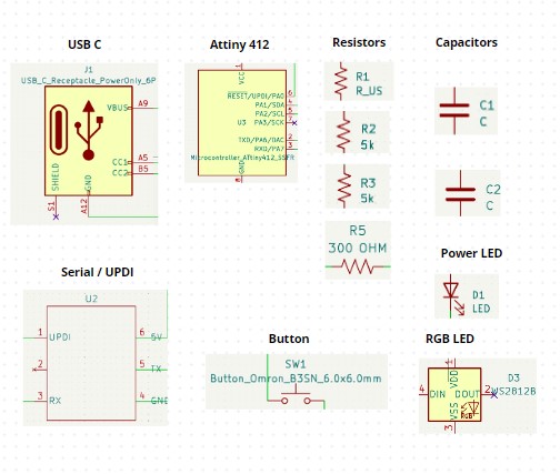
Features
- Attiny 412
- USB_C
- RGB LED
- Button Omron
- Resistors
- Capacitors
- UPDI-FTDI
- LED
Getting started
Download KiCad
Make sure you have at KiCad 6 or greater installed.
Add Fab’Academy’s library
Fab Electronics Library for KiCad: https://gitlab.fabcloud.org/pub/libraries/electronics/kicad
Steps
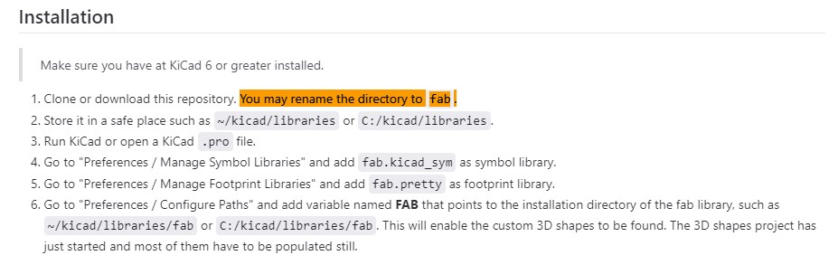
- Clone or download as zip this repository.
- Unzip it and rename the directory to fab.
- Run KiCad or open a KiCad .pro file.
- Go to
Preferences / Manage Symbol Librariesadd fab.kicad_sym as symbol library. - Go to
Preferences / Manage Footprint Librariesadd fab.pretty as footprint library. - Go to
Preferences / Configure Pathsadd variable named FAB that points to the installation directory of the fab library, such as ~/kicad/libraries/fab or C:/kicad/libraries/fab. This will enable the custom 3D shapes to be found. The 3D shapes project has just started and most of them have to be populated still.
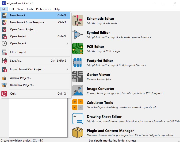
Create New Project
Click on FileNew project and save the file in the folder you desire.
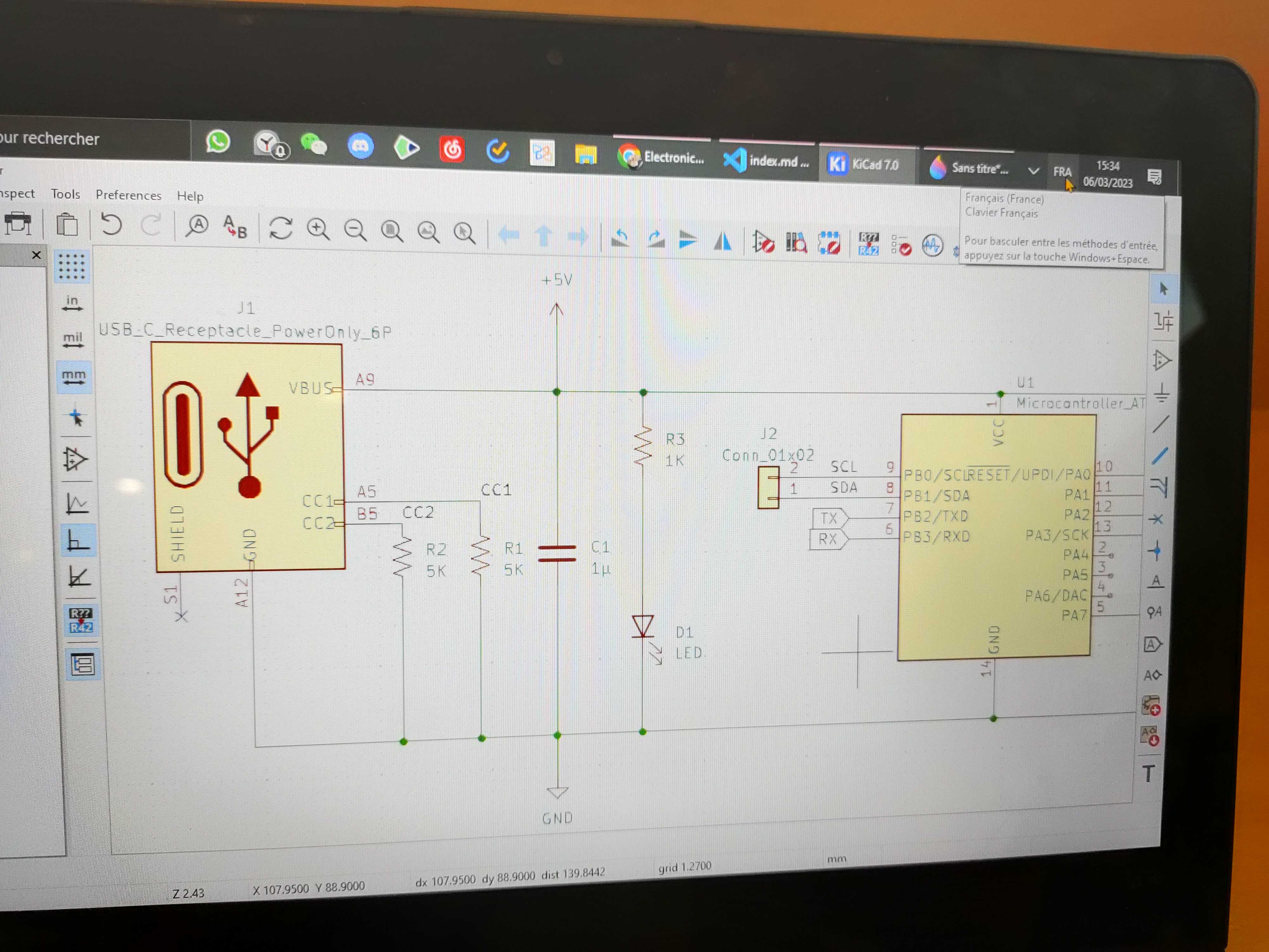
Schematic
In the schematic editor, we decided the type of component that we’re going to use and create link between components.
Button Add symbol
- OR keyboard shortcut

A
This will open the symbol library where we can add all the compenents we need.
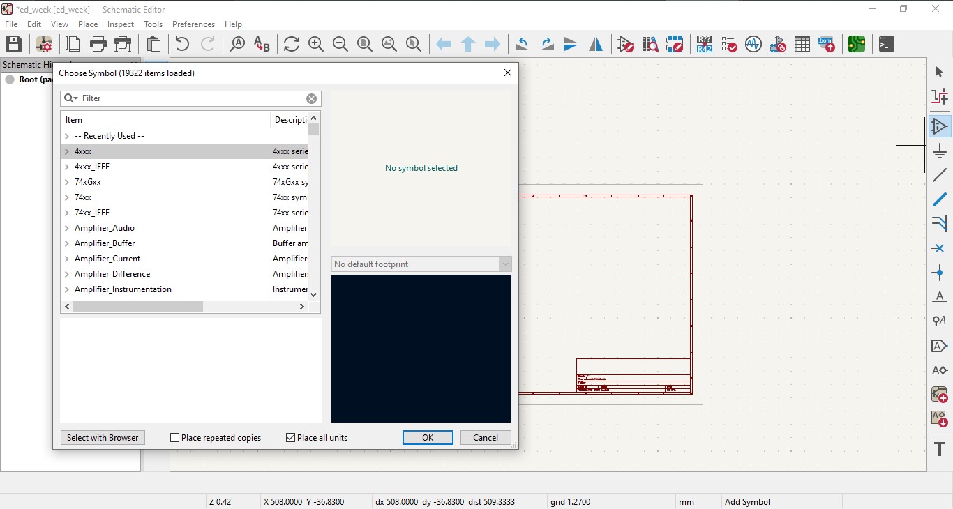
I added 12 components
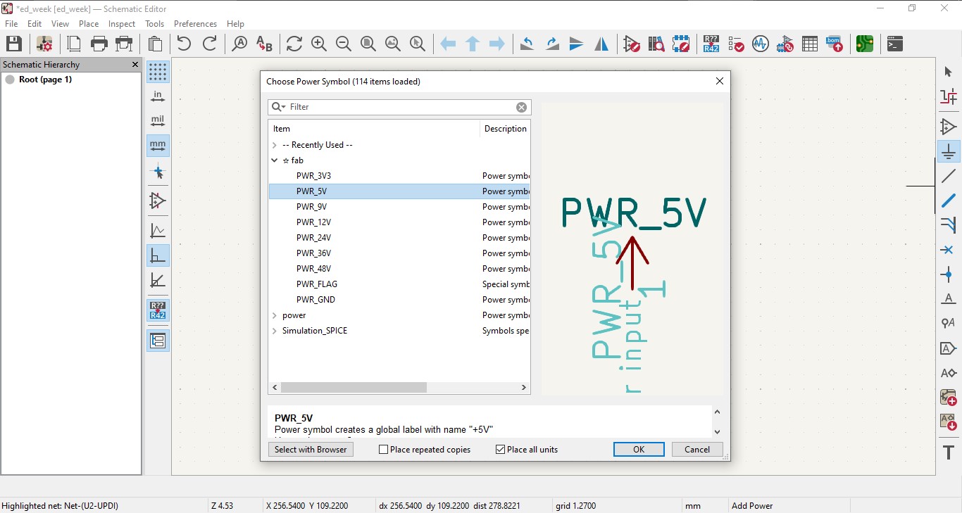
Add power symbol
- OR keyboard shortcut

P
This will open the Power Symbol library where you can add the power and the ground of your board.
Add wire
this will allows you to connect different components in your schematic.
Add net label
“Add Net Label” is used to label a net on a local schematic sheet By labeling nets, you can create a clear and organized schematic that is easy to read and understand. This makes it easier to design and modify circuits, as well as to troubleshoot and debug any issues that may arise.
Add global label
“Add Global Label” is used to label a net or group of nets that are visible across all schematic sheets in a project.
PCB Editor
Footprint Editor
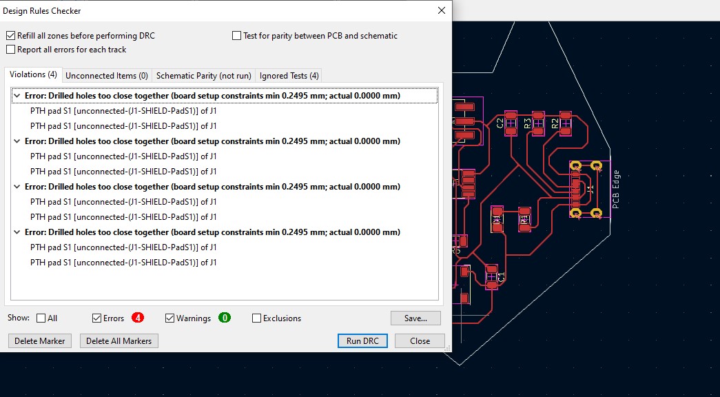
Problems and how I fixed them
-
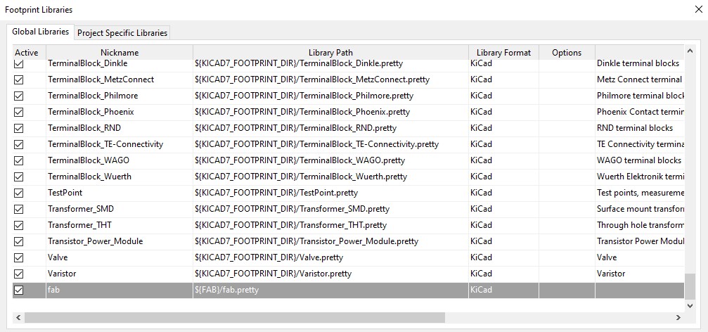
Changing the name of the directory of Fab Electronics Library AFTER setting it up.
When I finished my schematic, I saw on the git of the fab library that they reccommand to change the name of the directory to “fab”
Then, I changed the name
kicad-mastertofab. After that, I couldn’t find the footprints that are supposed to be here…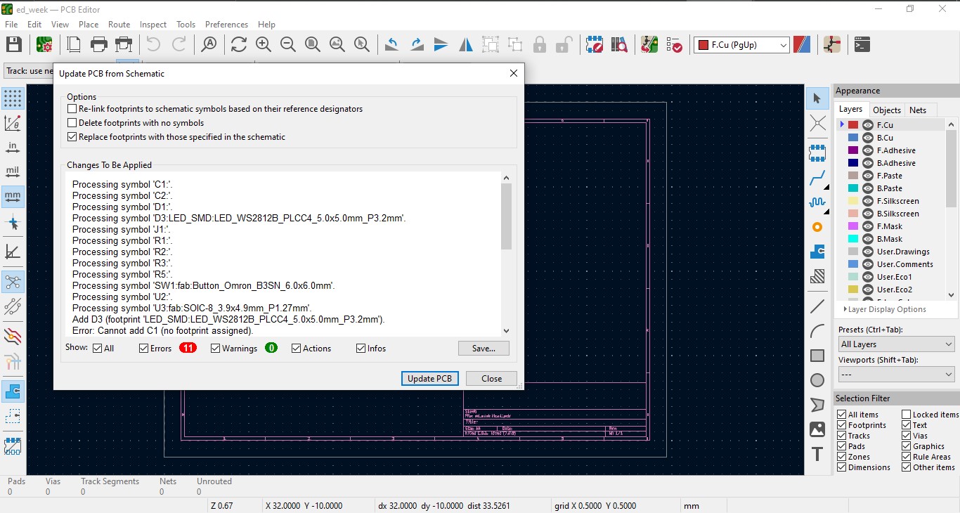
I fixed this by redirecting the path to the correct path name.
-
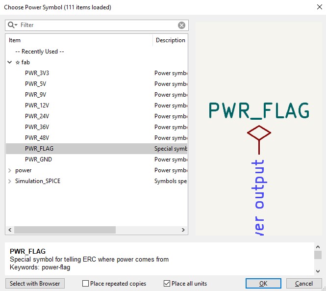
Error: Input Power pin not driven by any Output Power pins
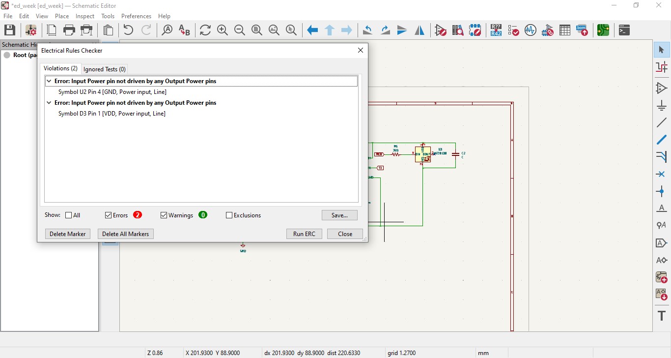
I looked for a solution on google and found this super documentation on kicad:
- [https://docs.kicad.org/master/en/getting_started_in_kicad/]https://docs.kicad.org/master/en/getting_started_in_kicad/getting_started_in_kicad.html#:~:text=In%20this%20case%2C%20KiCad%20reports,thinks%20the%20net%20is%20undriven.
It seems like KiCad thinks the net is undriven. I fixed this by adding power flag symbol to tell kicad where the power comes from.
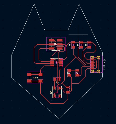
My First PCB.
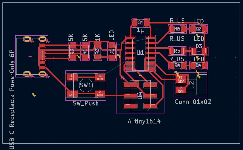
![]()
Hero shot
Original files
Group Assignment: Test equipments
The goal of electronic design, is to create a functional electronic circuit that operates reliably and efficiently.
The test equiments help us to make sure that the components are properly connected and that the signals can travel efficiently between them.
We go thought 3 different ways to do tests:
- Multimeter
- Oscilloscope
- Analyzer of signals
Our development board’s Features:
- Attiny 412
- LED
-
PWM
-
Multimeter
With the multimeter, we measured the voltage between terminals.
| Terminals | In theory | In practice |
|---|---|---|
| VCC | 5 V | 5.16 V |
| PWM | 0.2 V | 0.205 |
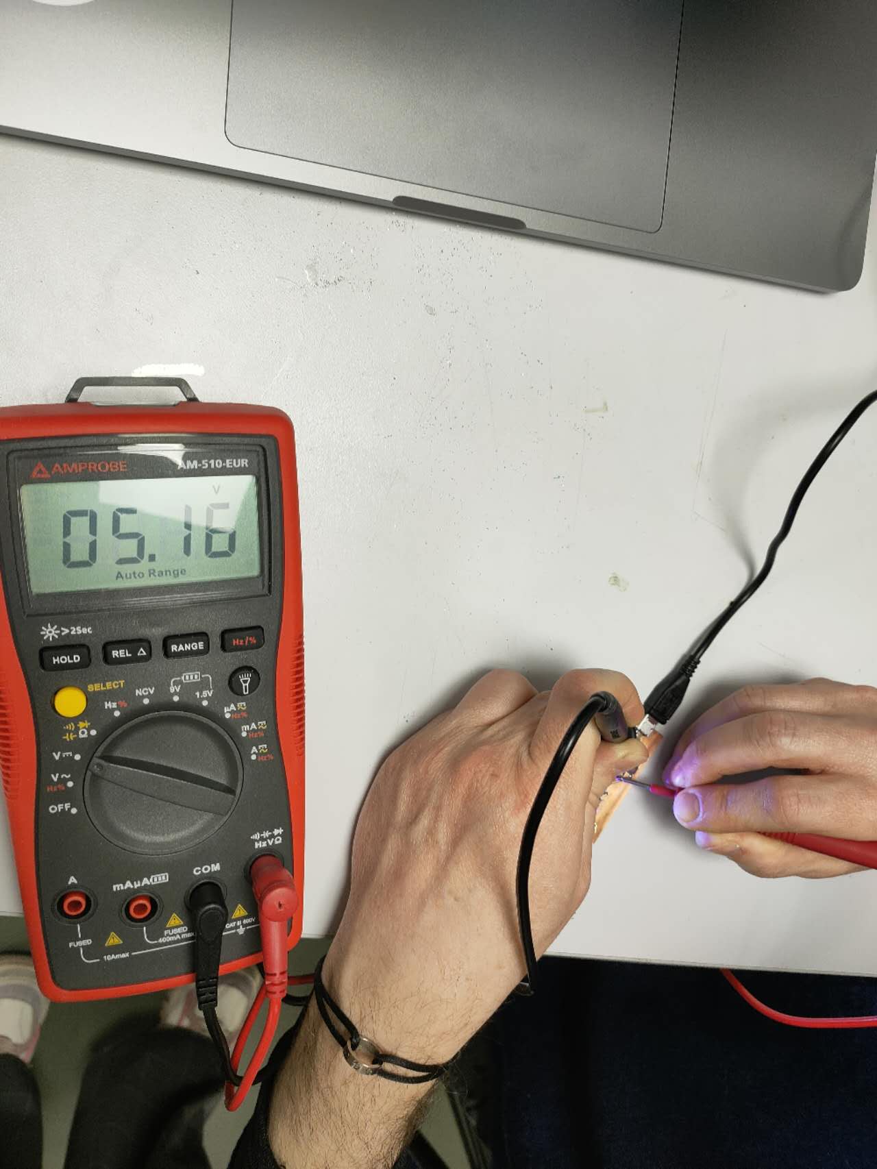
What can a multimeter measure?
Voltage: A multimeter can measure DC voltage, AC voltage, and AC/DC voltage with respect to ground or reference.
Current: A multimeter can measure DC current and AC current (using a clamp accessory).
Resistance: A multimeter can measure resistance in ohms, kilohms, and megohms.
Continuity: A multimeter can test for continuity between two points in a circuit to determine if there is a complete connection.
Capacitance: A multimeter can measure capacitance in farads, microfarads, and picofarads.
Frequency: A multimeter can measure frequency in hertz (Hz).
Temperature: Some advanced multimeters can measure temperature using thermocouple or thermistor probes.
Diode and transistor testing: A multimeter can test for the presence and polarity of diodes and the gain and polarity of transistors.
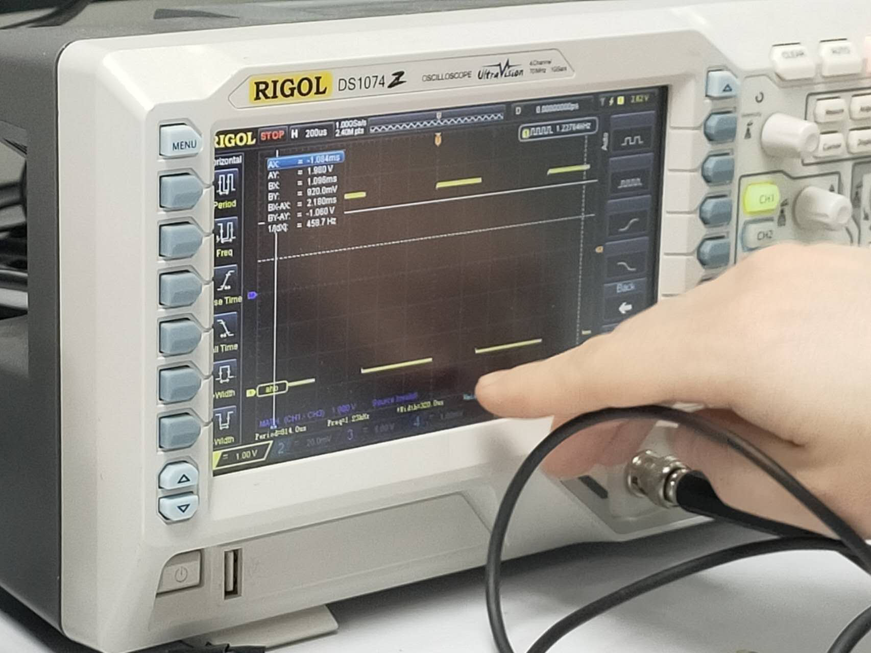
- Oscilloscope
We were using a oscilloscope to visualise the frequency of signal. We saw tiny interference.
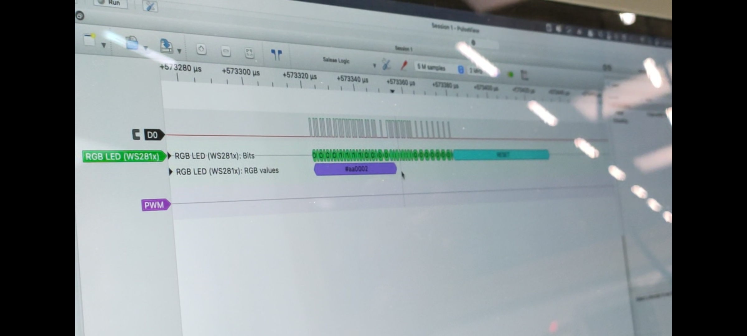
- Analyzer
Connected to a PC, this analyzer works with PulseView, a softwre that interpreter of digital signals.