WEEK 6
For this week assignment, I had to design my ESP-WROOM-02D development board which I will use for my final project.
ELECTRONICS DESIGN
Group assignment :
- Use the test equipment in your lab to observe the operation of a microcontroller circuit board (as a minimum, you should demonstrate the use of a multimeter and oscilloscope)
To see our group assignment click here
Individual assignment :
-
Design a development board to interact and communicate with an embedded microcontroller
-
Extra credit: try another design workflow; make a case for it; Simulate its operation
For the design of a printed circuit there are various software namely: Autodesk Eagle, Altium Designer, Proteus, Kicad, EasyEDA… In our case we chose the software Autodesk Eagle
In the following we will show how we designed our PCB with Autodesk Eagle.
To start our work we needed to get some previous request.
To install Autodesk you can find all needs here
Installation of libraries
Libraries are what we need to own all necessary components to design our board in Autodesk Eagle.
For the realization of our printed circuit with Autodesk eagle we have downloaded the Fab libraries and the sparkfun libraries.
here’s how to get it :
after that extract the zip file then copy .lbr and .dru to the directory : Documents>EAGLE>libraries. Use this links to get more infos about fab libraries and sparkfun libraries installation.
Prerequisit
Before starting the design of our ESP-WROOM-02 D development board, we need to know all the basic components needed to make our microcontroller work. So we went to its datasheet where we can find some useful informations like these :
1. The peripheral schematic
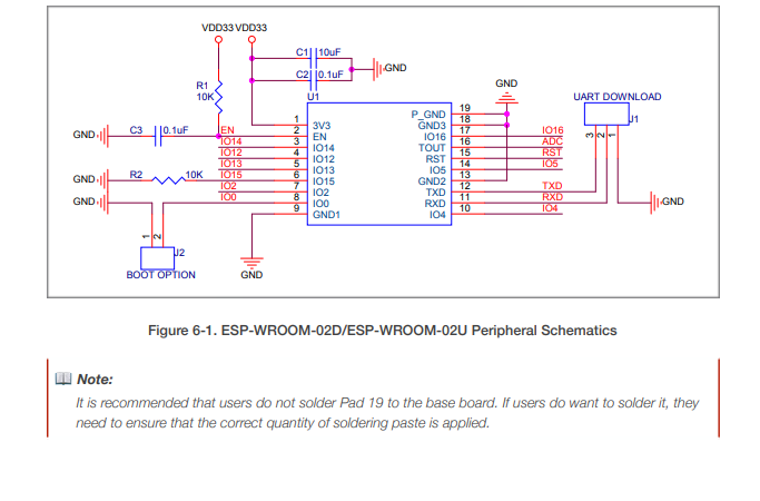
We can notice a note which says that it’s recommended to do not soldering the Pad 19, which is a good thing for me cause I didn’t know how to solder it 😶.
2. The Electrostatic discharge
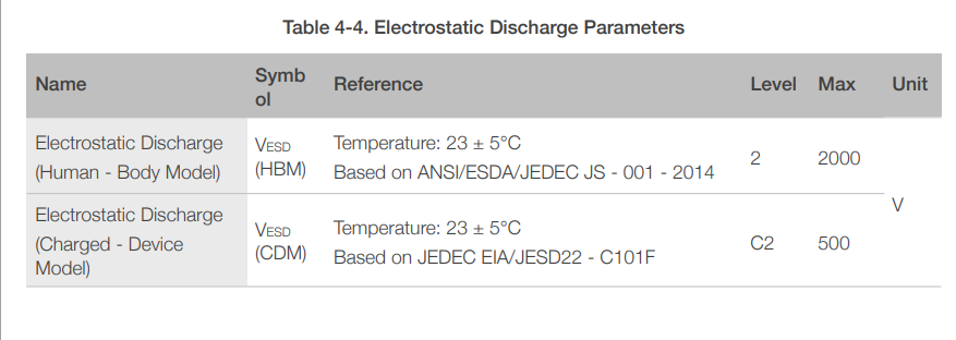
The ESD is a real enemy for some microcontrollers like this one 😯 hence it’s very important to be very careful when using. Cause we could short circuited pads of microcontroller.
3. some useful informations
these information are Electrical Characteristics, Power consumption. go to the datasheet to get these infos.
The Designing
From the datasheet and according to our objective the components we needed to design our board are :
| components | Quantity |
|---|---|
| - 6MM_SWITCH6MM_SWITCH | 1 |
| - V_REG_LM1117SOT223 | 1 |
| - Resistor SMD 100 | 2 |
| - CAP-UNPOLARIZED 100nF | 1 |
| - Resistor SMD 10k | 2 |
| - CAP-UNPOLARIZED 10uF | 1 |
| - CAP-UNPOLARIZED 1uF | 1 |
| - CONN_06_FTDI-SMD-HEADER | 2 |
| - ESP-WROOM-02FRONT-FACE | 1 |
| - Blue LED | 1 |
| - Slide switch | 1 |
| - SW_SPDTSWITCH | 2 |
For the last component we just added it to get the pattern, we won’t use the component.
As you know our board uses an ESP-WROOM-02D.the ESP-WROOM-02 has a few unique traits including: small form factor, affordable price, and the ability to write Arduino programs (it can be used as an Arduino) and to communicate over Wifi. For these reasons, more and more people are using this module in their projects.
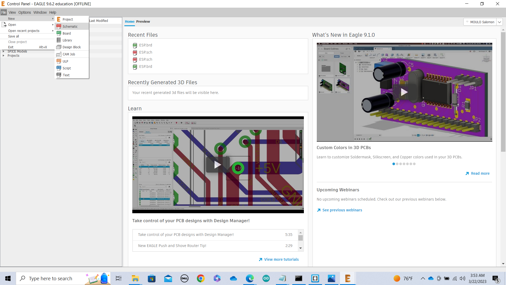
- Now Open Autodesk Eagle
We admit having downloaded all the necessary.
To begin, proceed like this :
click on File>New>Schematic as shown below
- Click on the “Add Part” button and select the “LEDFAB1206” component as shown below.
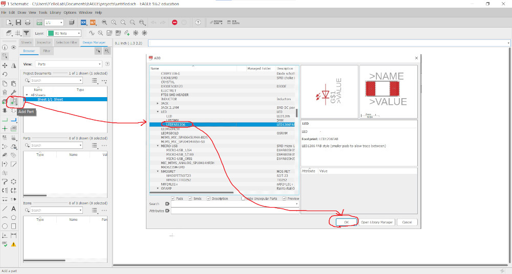
go to workspace and click there to place component.
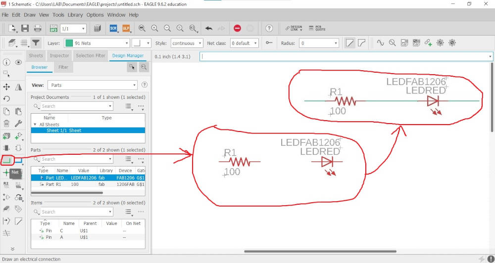
- After adding a second component which is a resistor click on “Net” to connect the different components as shown below.
-
Click on “Name” and rename the green lines as shown below. That is useful to connect two components without existing wire connections between them. It allows making clean schematics.
-
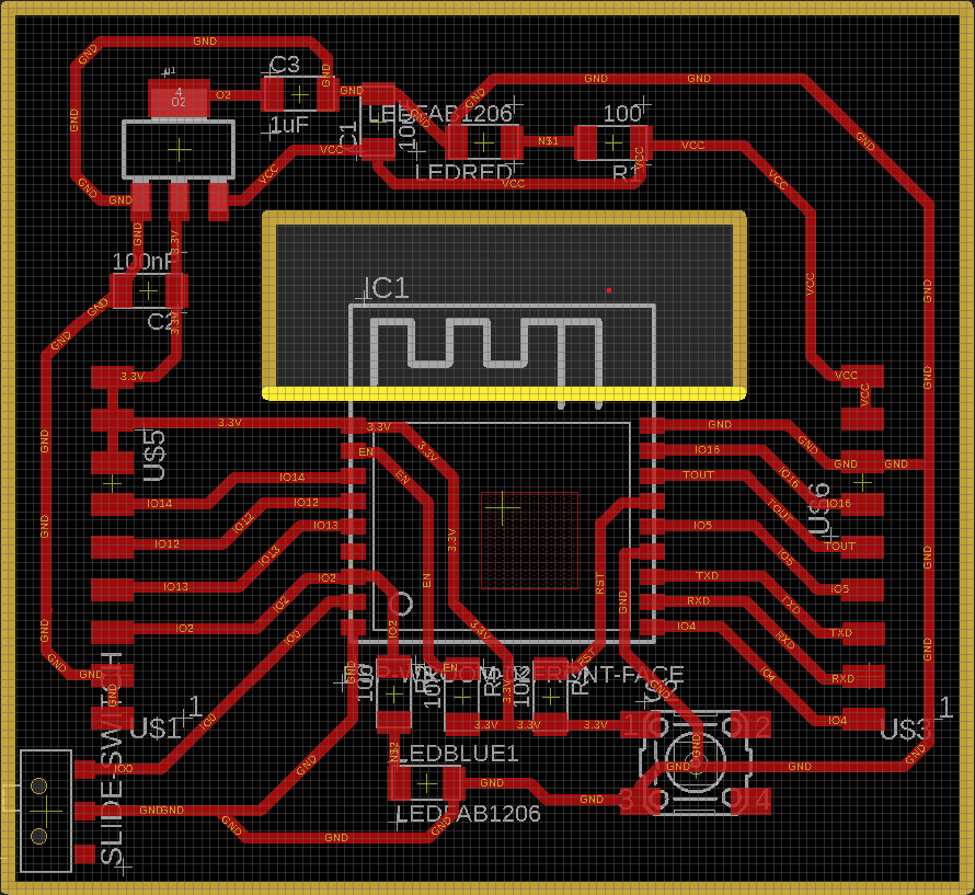
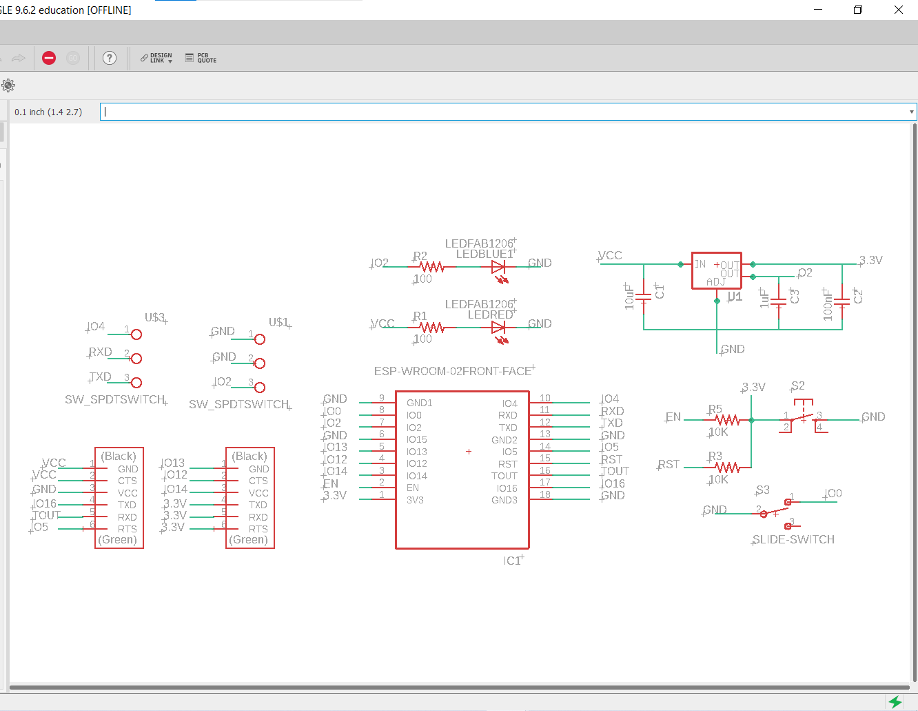
Repeat the same pocedure to draw all your schematic I finally made this :
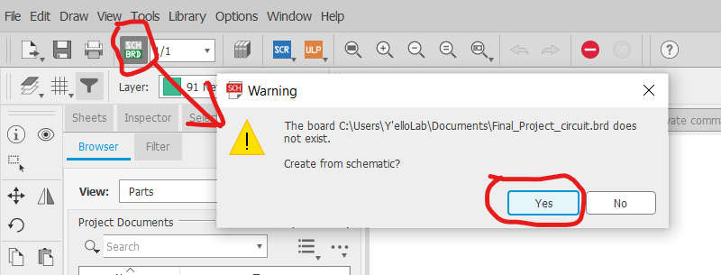
- When you finish schematics, moove to the PCB by clicking on “Generate/switch to board” button and click on “Yes” you should have the following display.
Use Edit tool then Design rule. In the appearing window click load then choose .dru files. Or if you don’t have any .dru file or use it you can arrange manually your components. Here’s a very useful link where you’ll find how to do that.
I finally made this :
Help
Use this link for helping you design properly your schematic.
I made some modifications concerning my board cause I encountered some difficulties to make my board work properly.
Hence I needed to design my board again from the one I’ve already done.
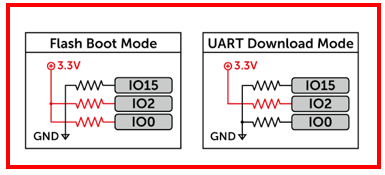
Before I was asking myself why my board didn’t work until I notice that I didn’t make properly the circuit of flash boot and UART download mode. Also I miss some components then I place them now.
This the schematics modified
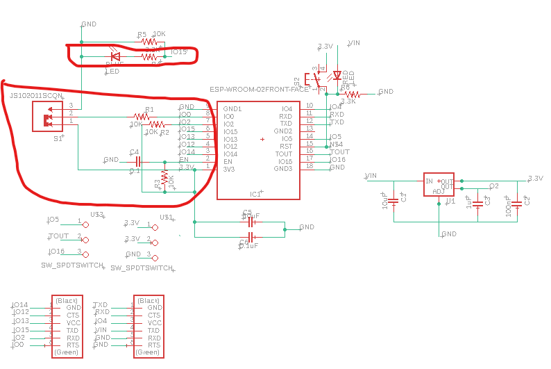
On the schematics I highlighted an error that I made to connect the LED work state what I should connect to IO2 and not IO15, then I also highlighted a part of circuit containing the circuit of flash boot and UART download mode.
As illustration, following is an image show how the flash boot and the UART download mode circuit should be.
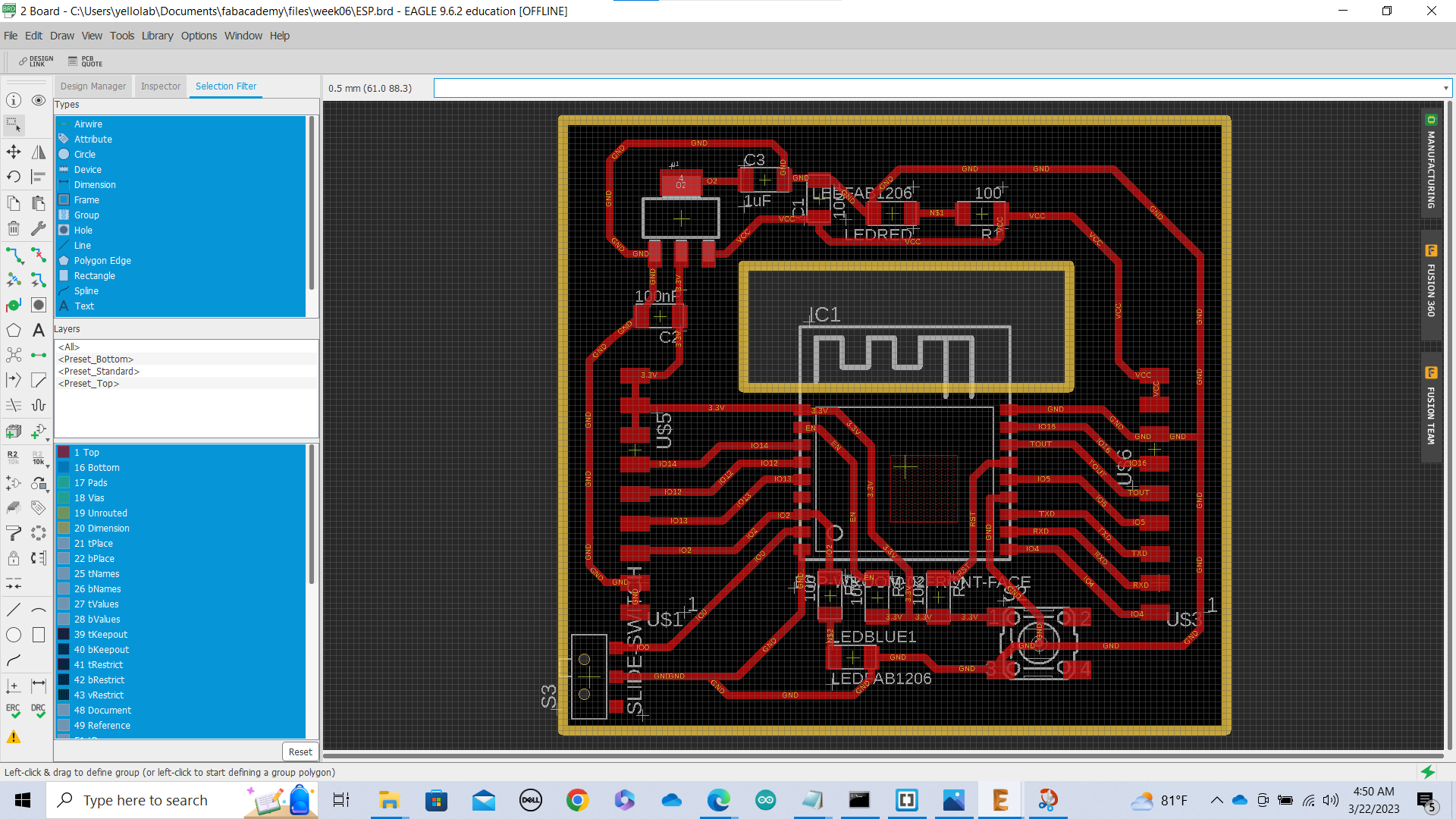
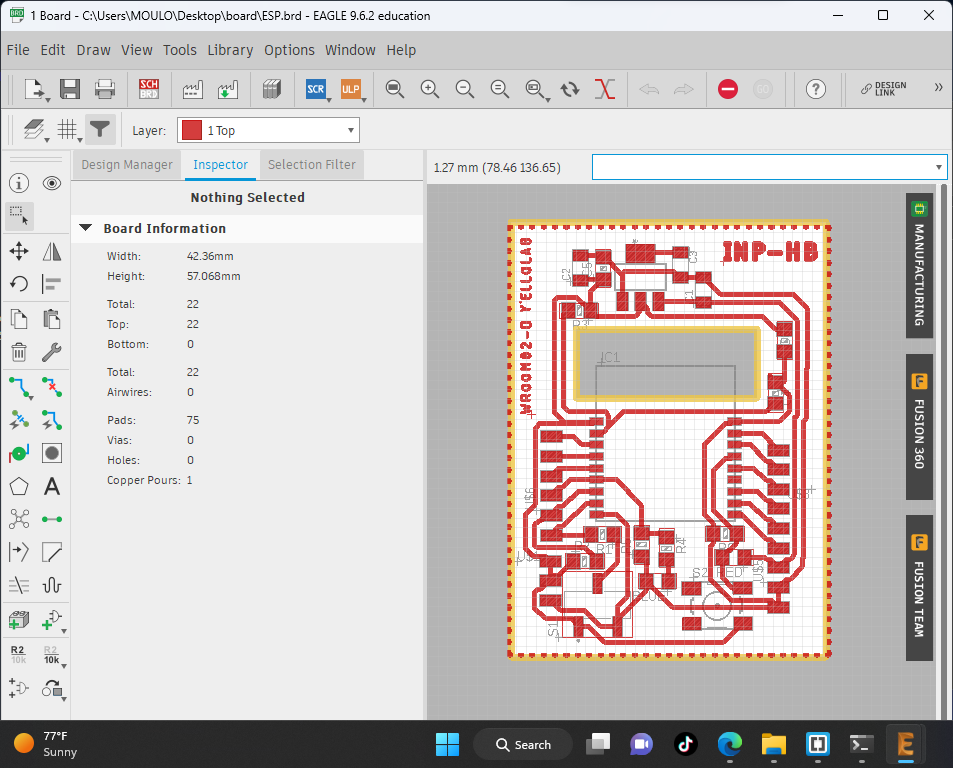
then I complete the board by making the PCB with generate PCB tool of Eagle. In the video below I show how I drew traces of the board.
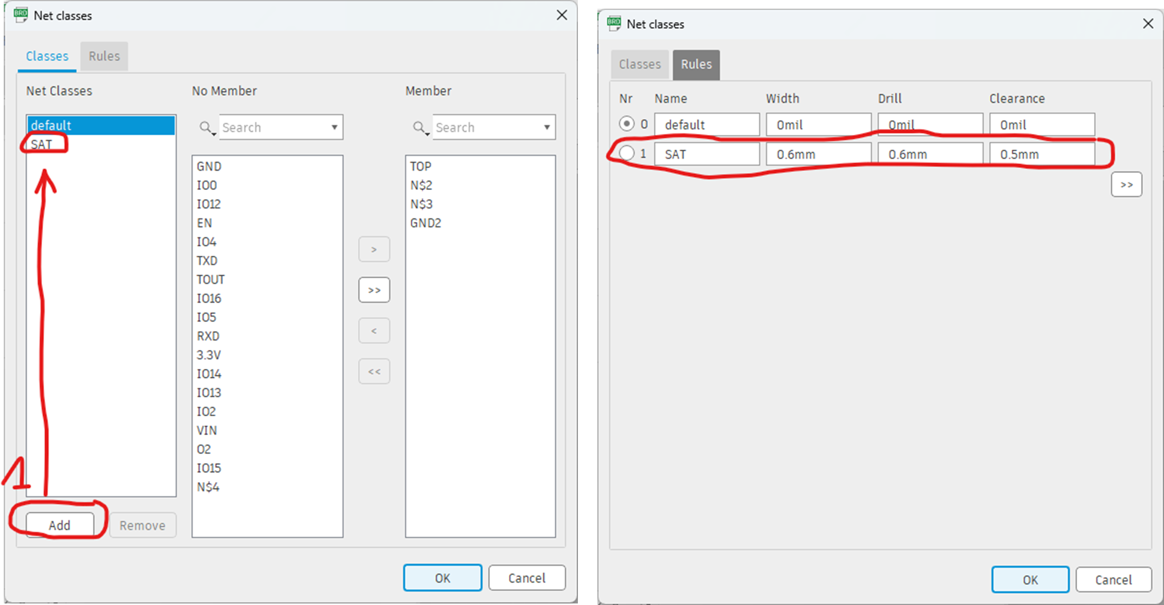
Board traces parameters
I set parameters for traces in the Edit box precisely Edit > Net classes. After click on net classes a Net classes window will open where we set rules of traces As gave in the table below.
| Width | Drill | Clearance |
|---|---|---|
| 0.6mm | 0.6mm | 0.5mm |
Width correspond to the width of the trace I decided to set it to 0.6mm because I’d like to have a quite large trace on my board.
Drill is where the tools(borer) will pass trough to mill. The tool I used is 1/64” i.e around 0.4 mm So I can set until 0.4 mm of drill parameter.
The clearance refer to the space between patterns. It is preferable to not set less than the tool diameter.
In my case I created my own net classe which I set different parameters as highlighted below.
This is the final result show below
Here’s a .zip file where you’ll find all my work : The board schematics
the New one is here