6. Electronics design
This week we searched PCB editor, general electric laws and electronic design rules, also Multimeter. Decided to follow tutorial with more complex electric scheme to be sure than eventualy I will understand how to attach everything I need.
Documentation
- KiCad is a free and open source cross-platform EDA-class software package designed for the development of electrical circuits and printed circuit boards. Decided to use it, because it is one of the most common softs, so make sence to invest time in studing to use it.
- Kicad include few soft components
- kicad - project manager
- eeschema - editor of electrical circuits
- Creation of single-sheet and hierarchical schemes
- PCB routing check (ERC)
- Creating a netlist for the pcbnew board layout editor or for Spice circuit simulation
- Access to the documentation for the electronic components used in the circuit (datasheet)
- Built-in editor of schematic symbols (library components)
- pcbnew - printed circuit board editor
- Development of boards containing up to 16 copper layers and up to 12 technical layers (silk-screen printing, solder mask, etc.)
- Access to external connection tracers by generating a board description in the Specctra Design Language (on-line FreeRoute, etc.)
- Generation of technological files for the manufacture of printed circuit boards (Gerber files for photoplotters, drilling files and component placement files)
- Layer-by-layer printing of circuit diagrams and drawings of printed circuit boards on a printer or plotter (in PostScript, HPGL, SVG and DXF formats), with or without a format frame
- Built-in footprint image editor (library components)
- 3D Viewer - 3D PCB viewer based on OpenGL (part of pcbnew)
- gerbview - viewer for Gerber files (photomasks)
- cvpcb - a program for selecting footprints corresponding to the components on the diagram
- wyoeditor - a text editor for viewing reports
- Decided to use Programmer-SWD-D11C, because was sure that will manage soldering.
- "A" - to define components.
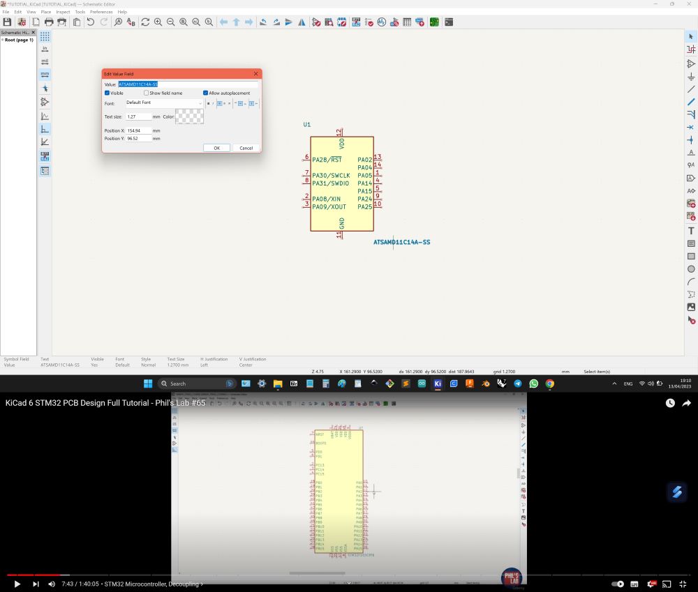
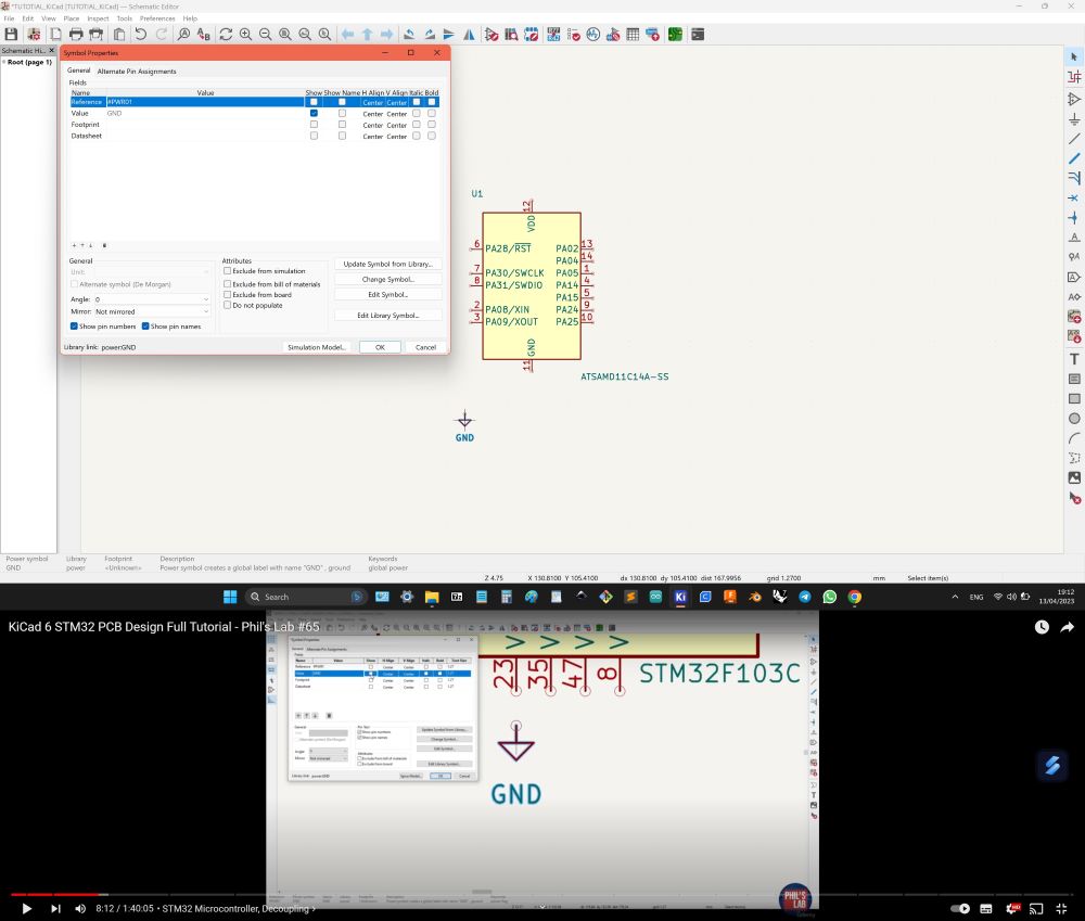
- "P" - to define power sourses and ground.
- Started from additing symbols of microcontroller and ground with power sources.
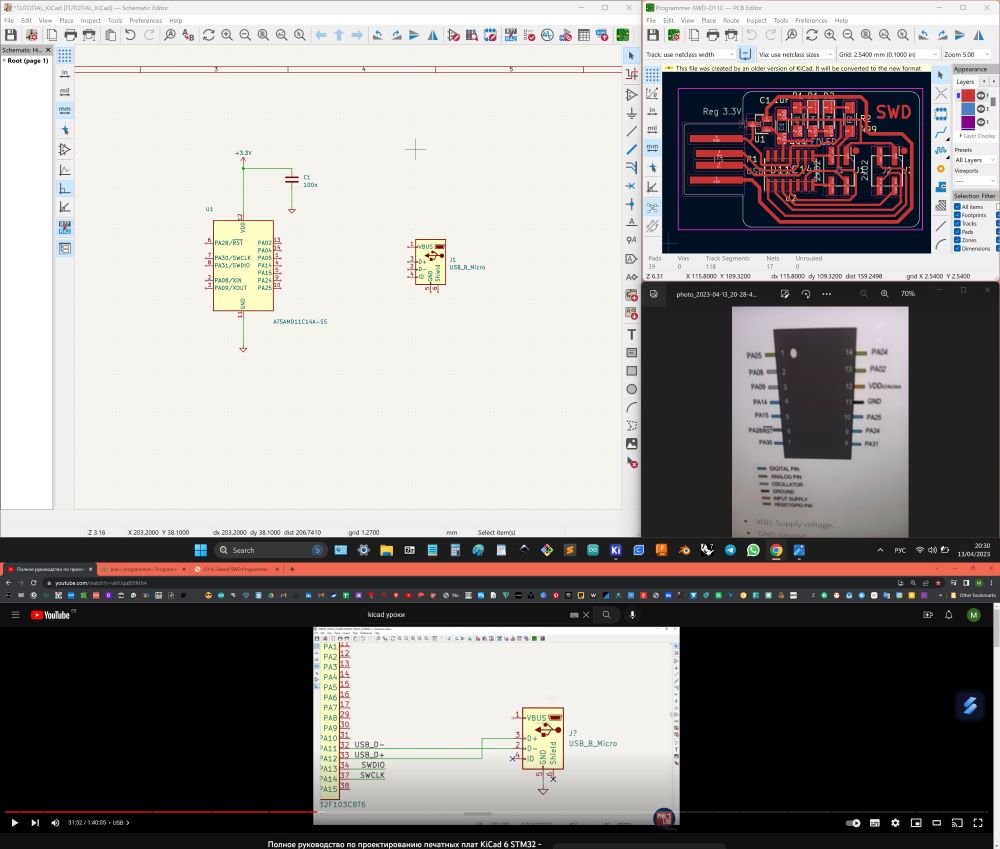
- "W" - for components connection on scheme (define relations between components to construct traces between them on PCB edition step) Datasheet needed to understood which pins needed.
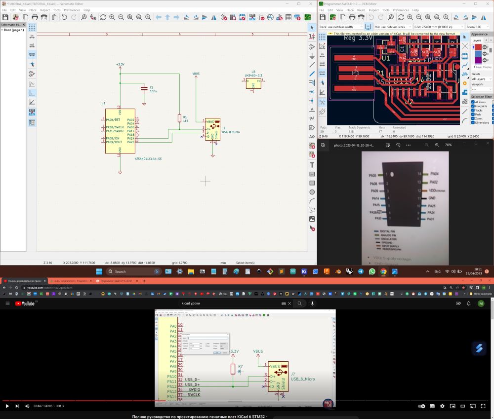
- "E" - for elements properties setting.
- Convinient to use both for organising scheme visually and editting functionally.
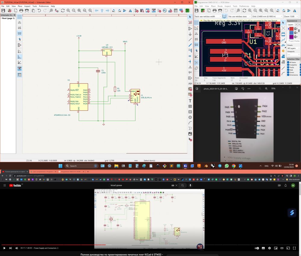
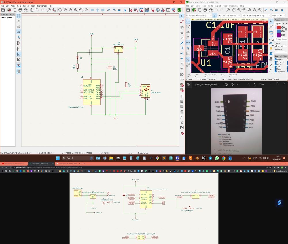
- Later I understood that scheme shoud be much more easy to understand, this tutorial gave understandung how to include mini-USB and capacitor (for stabnilisdation of microcontroller-components interaction voltage drops). Also used SAMD11C PCB board example to include voltage controller acurate.
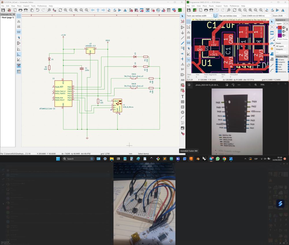
- Composed board correllating to breadboard.
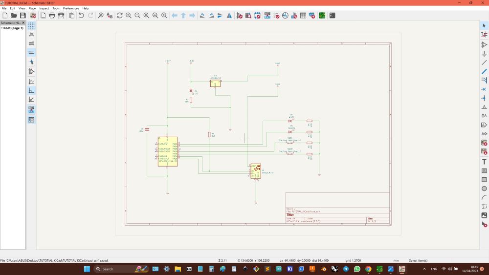
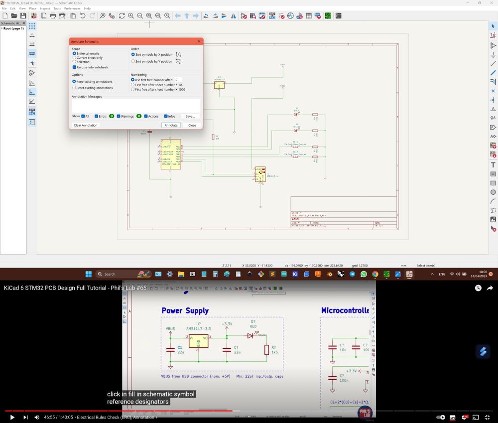
- After scheme was ready, setted annotations, because during editting components were moved and rotated, so anotations became random, that make PCB editing more difficult.
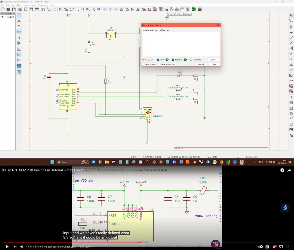
- After checked scheme on rough mistakes correleating to PCB rules (rules of electronics design).
- Some of mistakes and warrnings checks:
- Part assigned to component but not used
- Duplicated connection pins
- Duplicated equipotential in same location
- List of components which have duplicated parent symbols
- Empty terminal strips
- Equipotential conflict
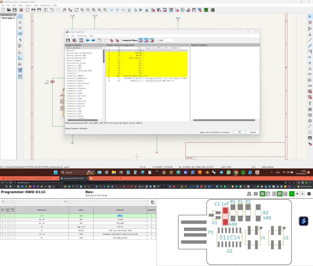
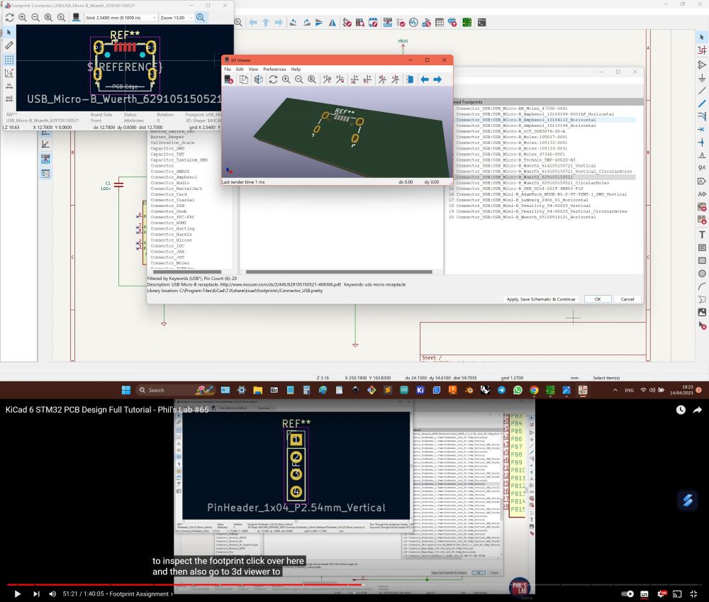
- After checked and defined footprints for components. This took some time, till I did not found how open visualisation and 3D model of footprints.
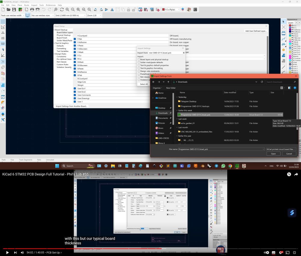
- Understood that not sure which general settings should be, so decided to import it from example PCB file.
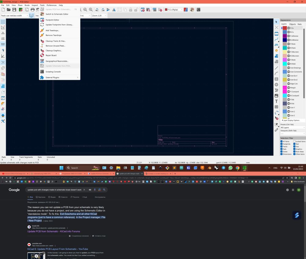
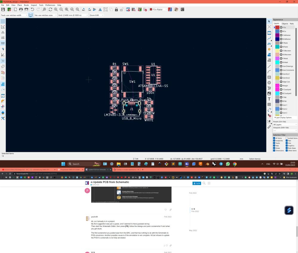
- PCB editor button in KiCad interface was not working for some reason, so found shortkey to update PCB with scheme changes ("F8").
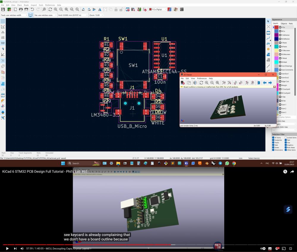
- "View" -> "3D view" - to see 3D visualisation of board.
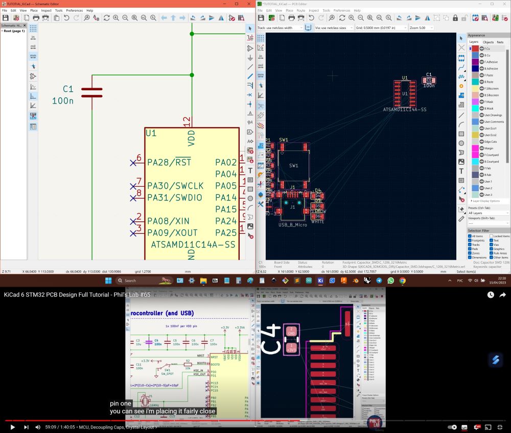
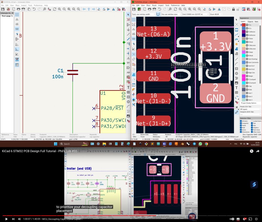
- Started to compose components, placing it how footprintes would be cutted.
- "CTRL" + "SHIFT" + "M" - measure tool.
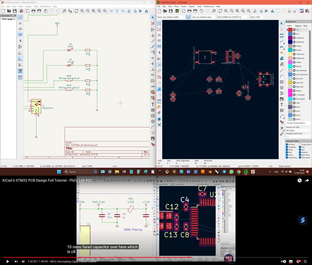
- Grouped them.
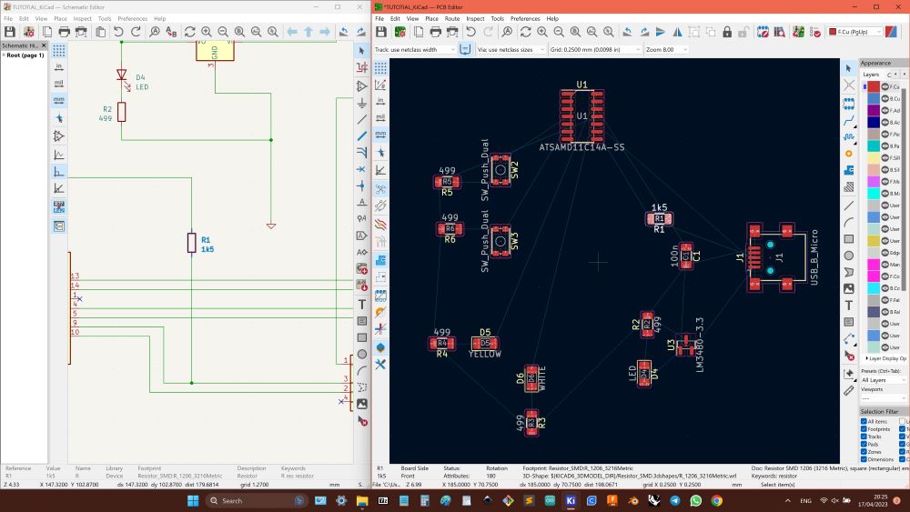
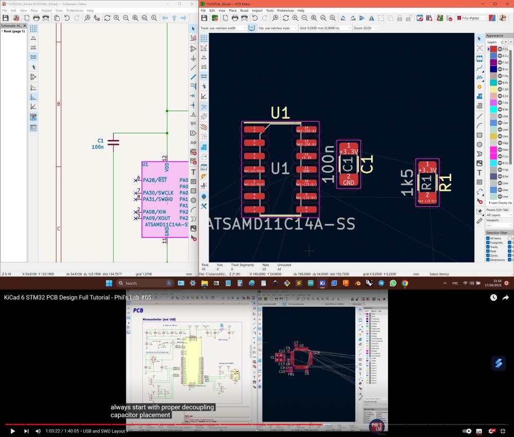
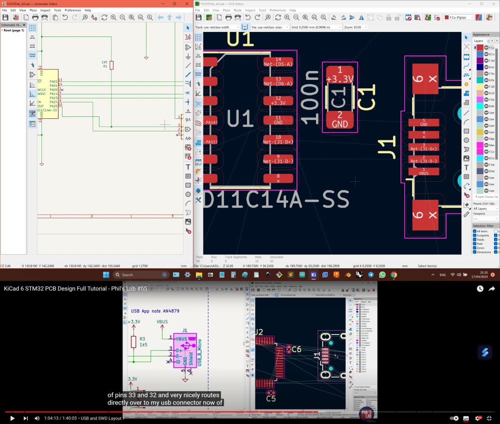
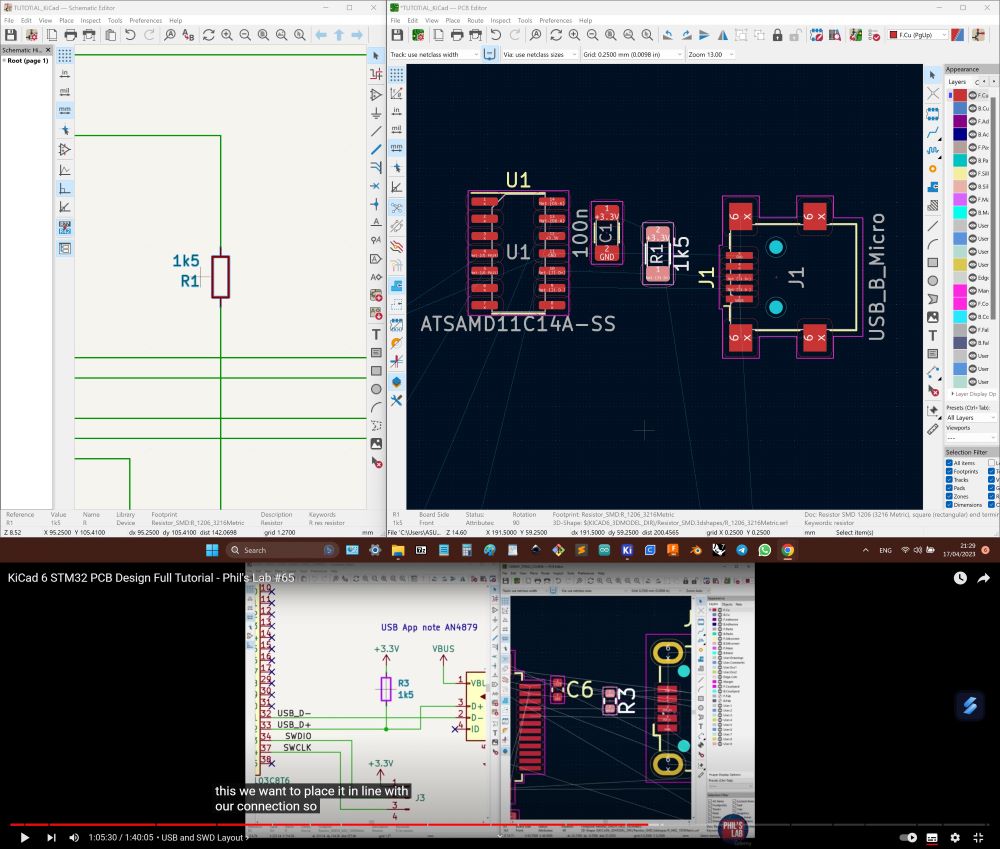
- Arranged microcontroller, capacitor, resistor for USB and USB correleating to tutorial. Capacitor should be placed near microcontroller to minimise noise, D+ / D- (differential pair) better to be same length.
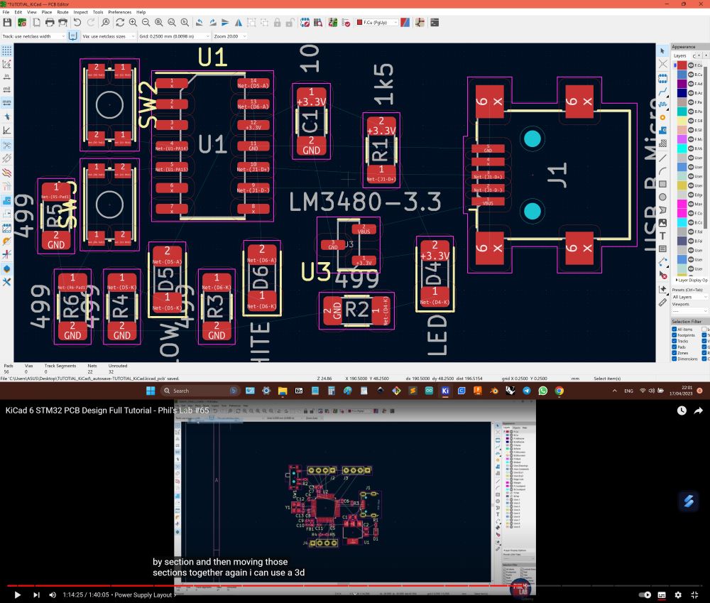
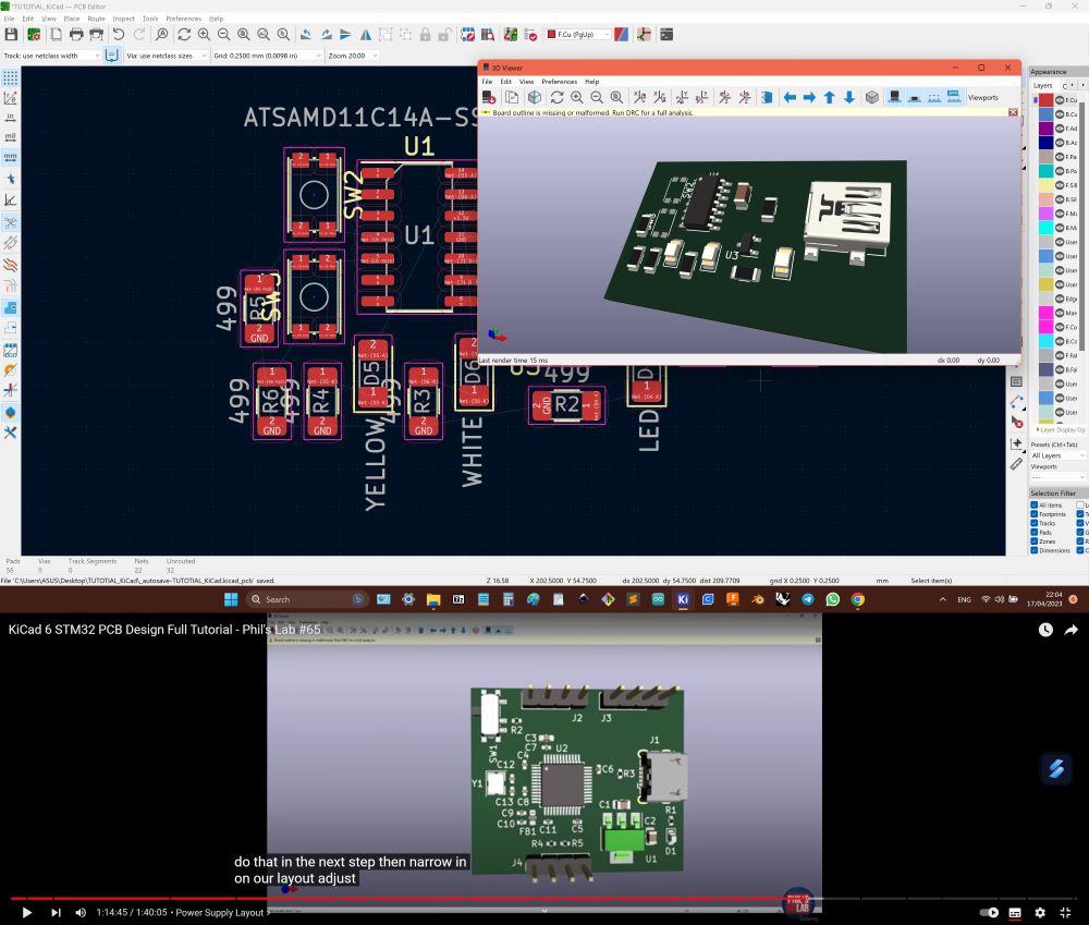
- Grouped components basing on scheme, checked how it lookes.
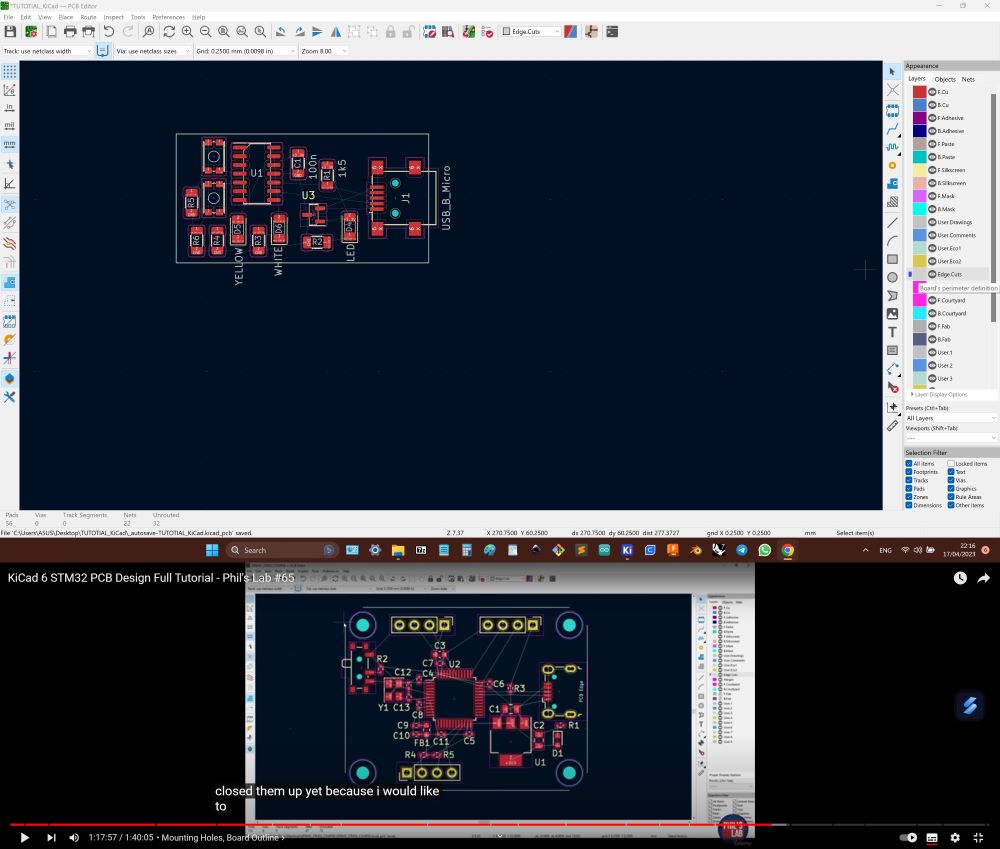
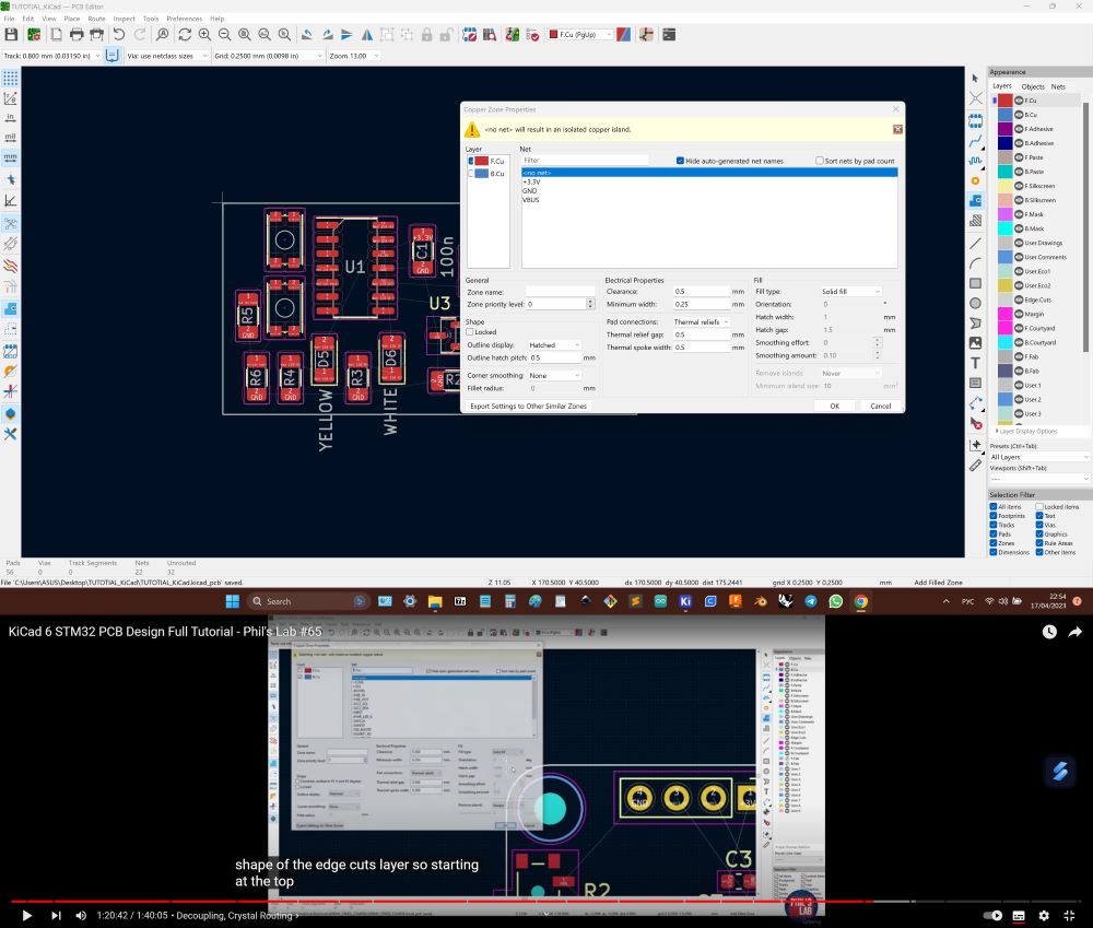
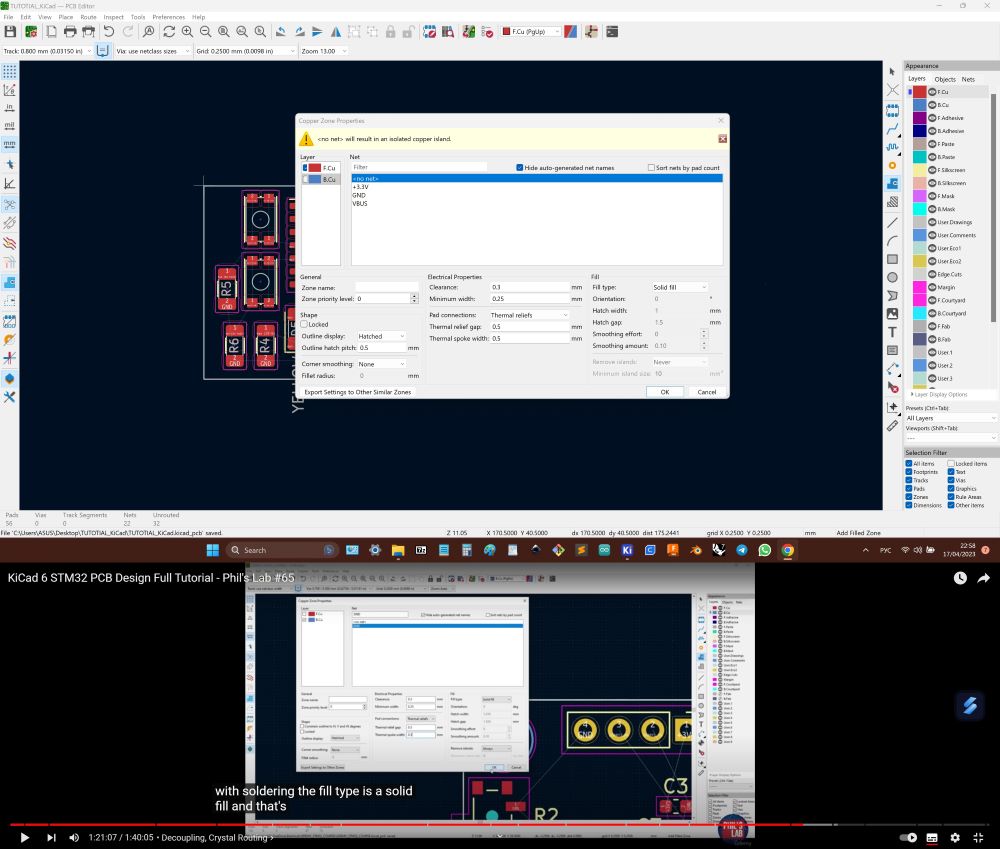
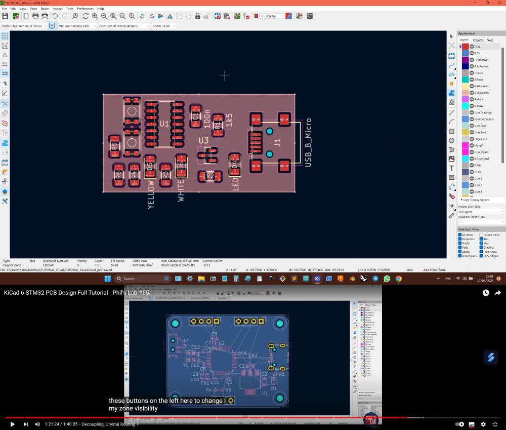
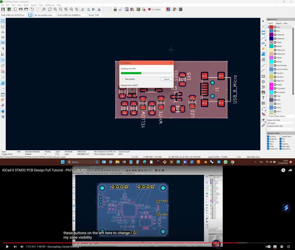
- Created edges for cutout and following tutorial created layer for another production process, so in that case (just cutting on mini CNC) it is not needed.
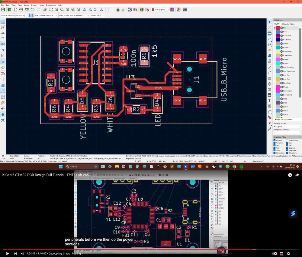
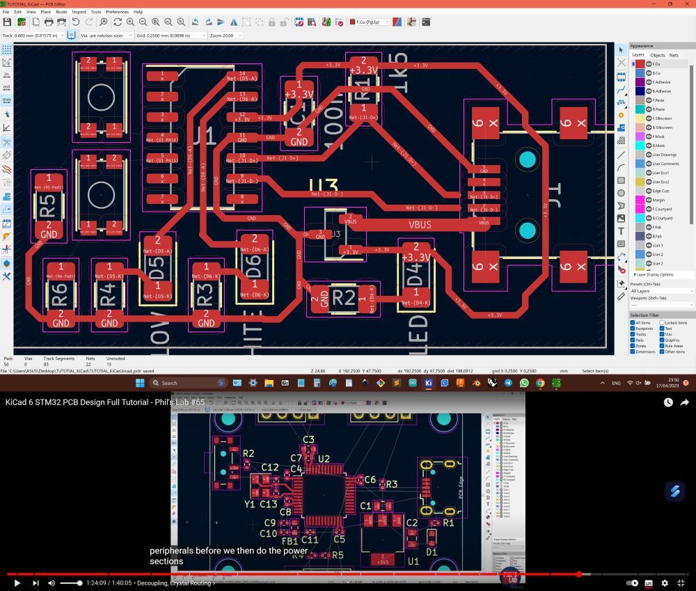
- Started to create traces (orienting on thin blue lines visualising connections defined in scheme).
- "X" - creation of phisical connections between footprints.
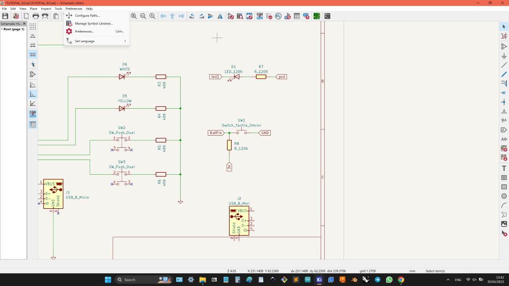
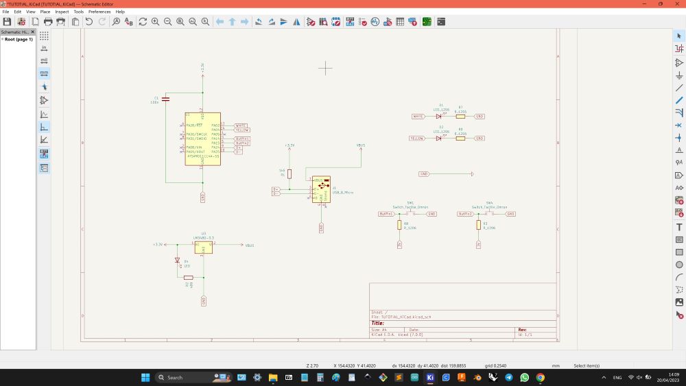
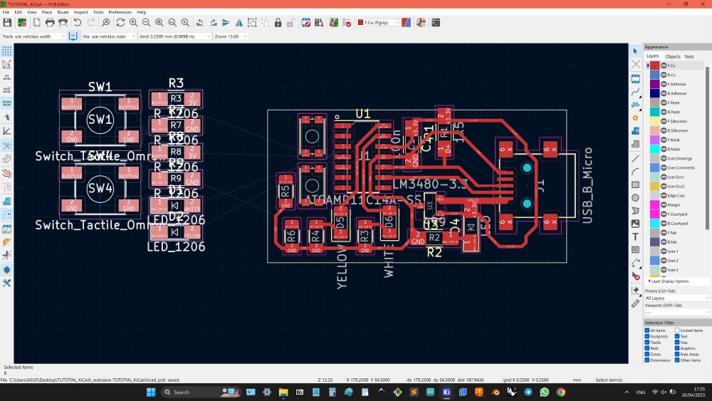
- After, I was told that choosed by me footprins were not correct, because of size, they were to small for soldering by beginner, so downloaded FabLab library and redefined footprints and PCB uploades. Also made scheme more easy to read.
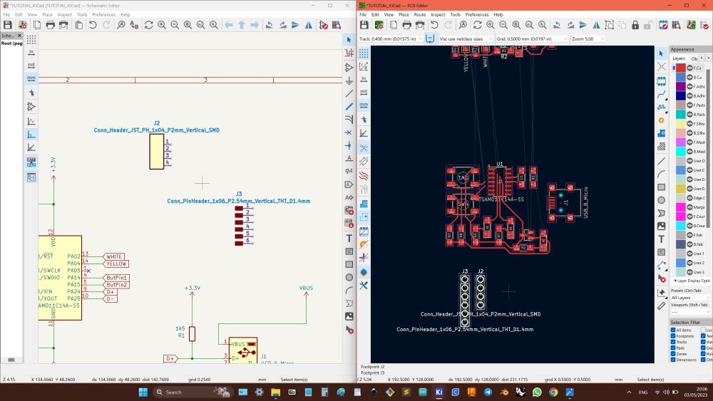
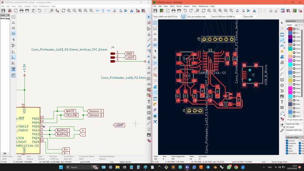
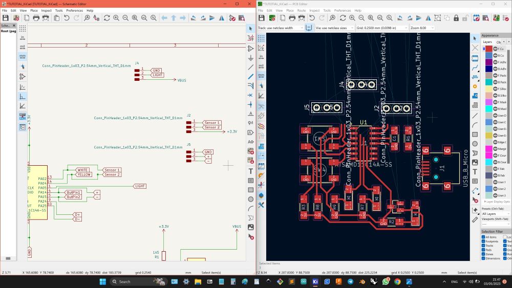
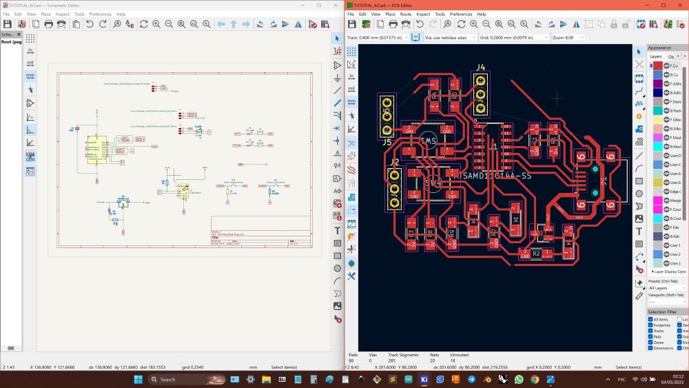
- Tried design board connecting all needed pins, but faced disability (ground and +3.3 lines were intersecting anyway).
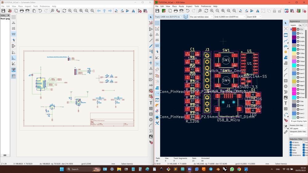
- In result decided to start from begining.
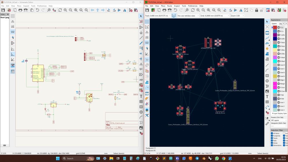
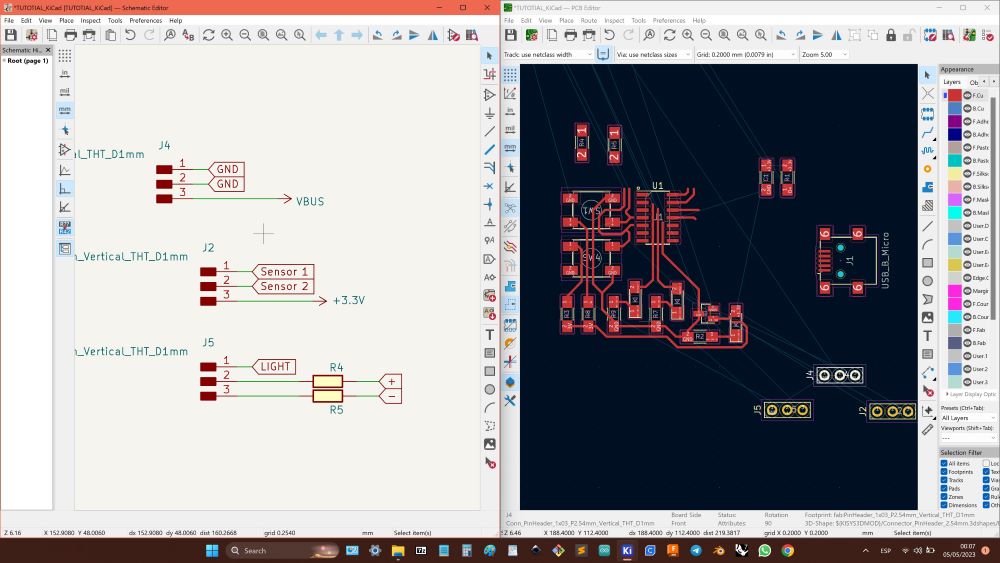
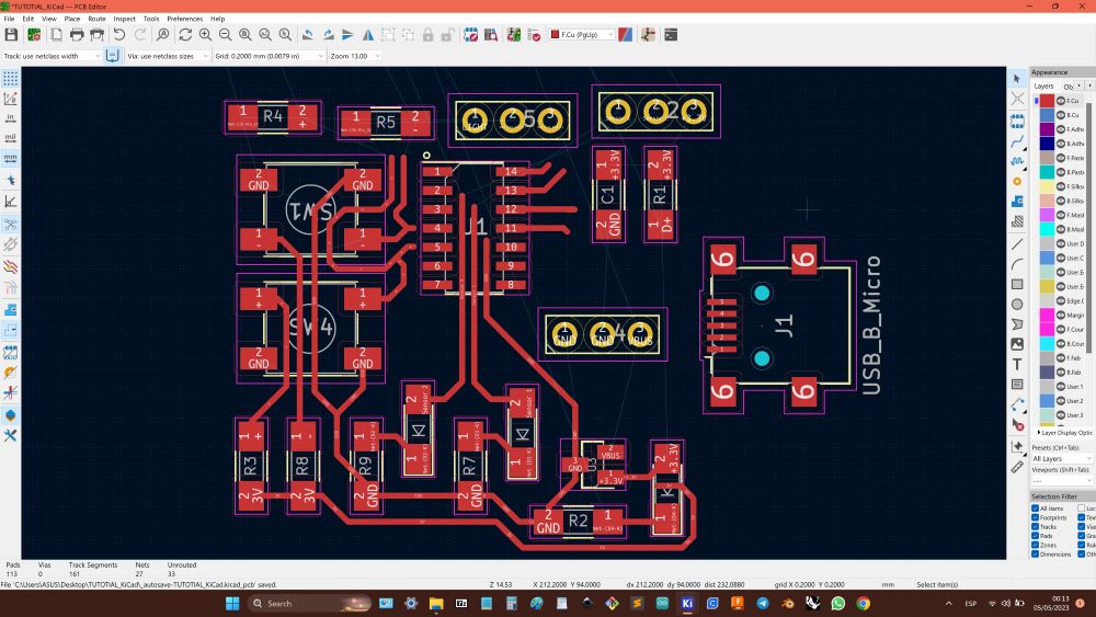
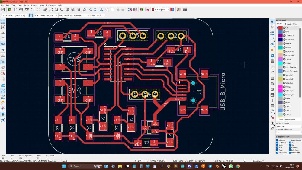
- Decided to complain board generally same way, but spliting pins another way.
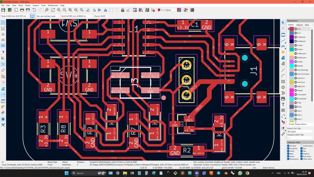
- Fogot about pins(4) for programming SAMD11C. Added, that made tracing more branching and curving.
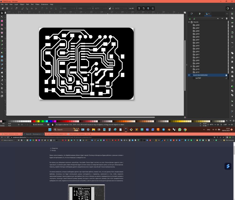
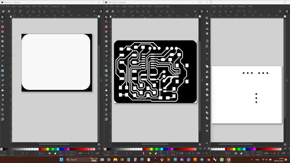
- Regard to group assignment documentation, edited SVG vectors by Inkscape, to define cutting and safe zone.