Week 4. Electronics production
I had never printed a card for a printed circuit using a milling machine, before I had done it by marking with indelible marker and ferric chloride, that was the instruction for this week, we were given the Quentorres plate in the course, then of testing with the use of equipment with values where we experienced failures and errors, especially in calibrating the z axis for the final marking on the plate. And that was not all, then I experienced, after a long time ago, soldering the components on the board with flux and tin along with the base of the microcontroller.
Group assignment:
- Characterize the design rules for your in-house PCB production process: document feeds, speeds, plunge rate, depth of cut (traces and outline) and tooling.
- Document the workflow for sending a PCB to a board house.
- Document your work to the group work page and reflect on your individual page what you learned Below we will show the work done with respect to production electronics
Individual assignments:
Make and test a microcontroller development board.
=======================================================
Group assignment:
On this occasion I had to travel 2 and a half hours from Cerro de Pasco to Huánuco to meet with my colleague Ronal and learn and test the operation of the cnc machine.
Learning Outcomes
- Described the process of tool-path generation, milling, stuffing, de-bugging and programming.
- Demonstrate correct workflows and identify areas for improvement if required.
For the group work I had to travel to the city of Huánuco, which is 121 kilometers away, to meet with my fellow student Ronal Vilca to acquire new knowledge as a result of working as a team, which I share in the following Link
Individual Assignment: Quentorres PCB
Gallery
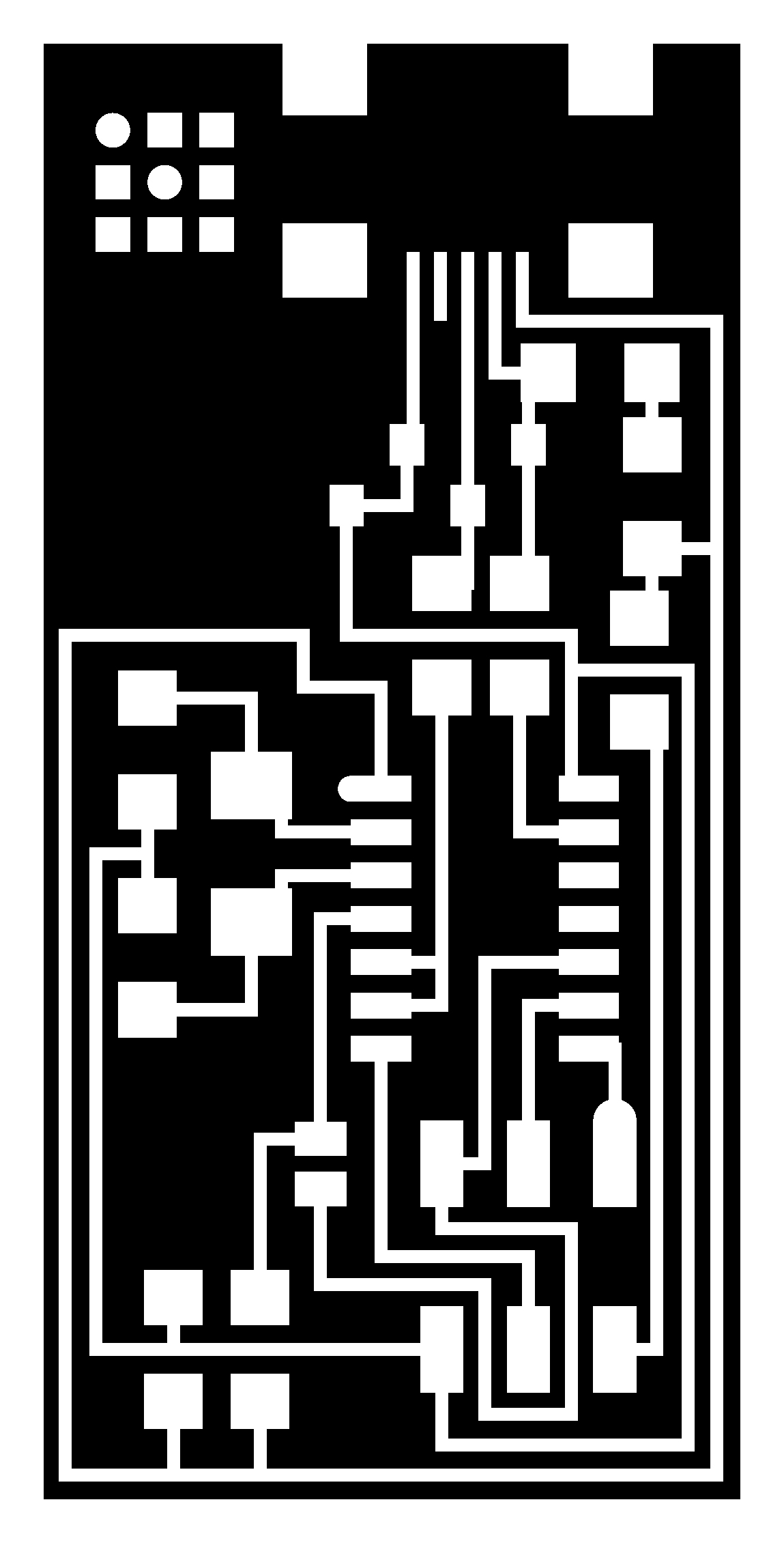
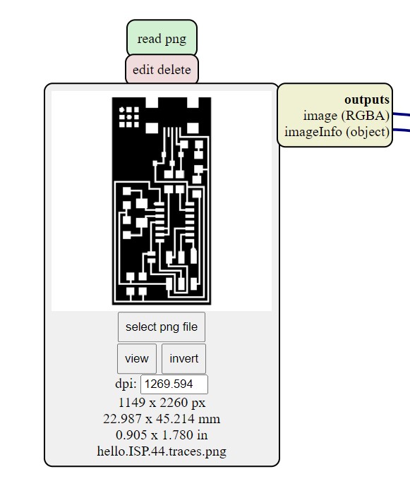
 In this image it corresponds to the impression of an example for the milling machine.
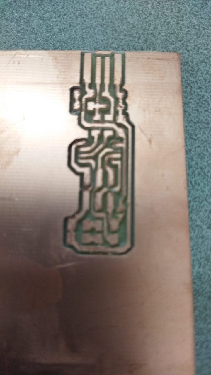
 The following image shows the final finish after the milling machine
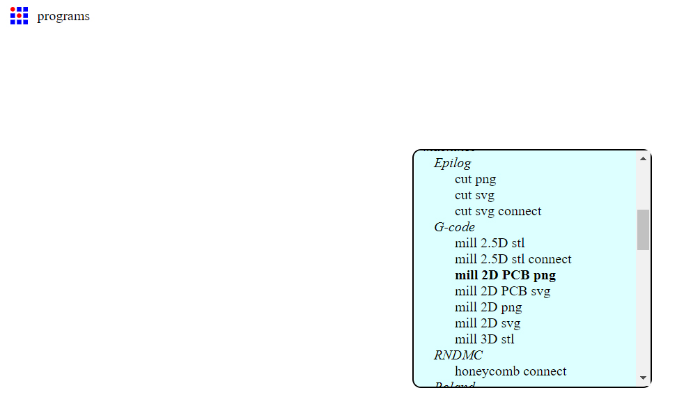
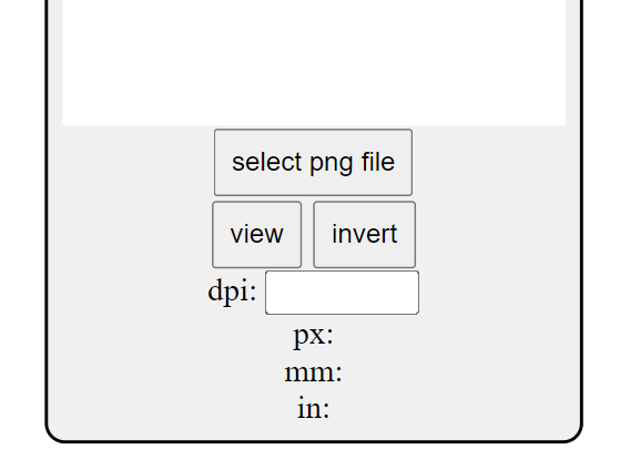
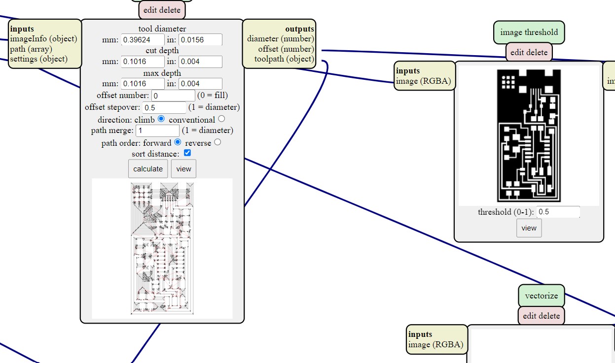
 After choosing the programs option, it shows me the following image.


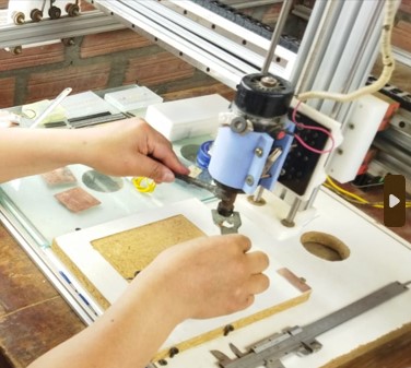
Below is the milling of printed circuit
===================================================================== This time we are going to describe the group work that was done with Ronal. To do this, I had to travel from the city of Cerro de Pasco to Huánuco.
A frezing machine has been identified made by our colleague Ronal, who already has experience in the assembly of the structure, motors and other elements that make up the equipment. Each component has been identified, in this photo the change of the spawn according to the needs is shown. In addition, the material that has been published on the website https://gitlab.fabcloud.org/pub/programmers/quentorres That allows you to load the gerver file, among others, on your computer.
 This image shows the printed circuit board, which will be cut with a saw blade for the scrubbing of the provided circuit.
 The following image shows the test of the screeding according to the model provided in the fab
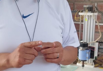
 A closer look at the fringe.
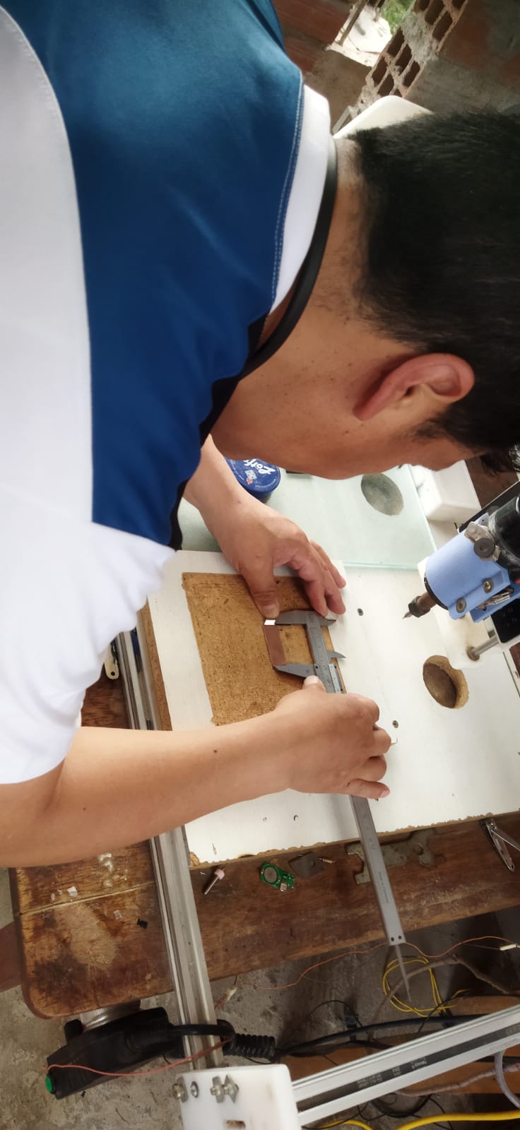
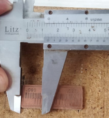
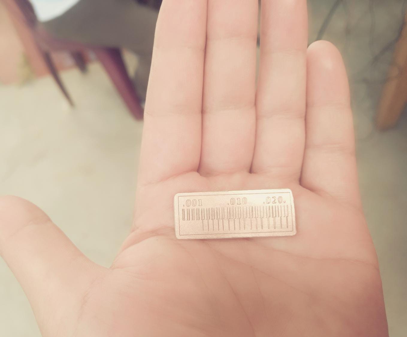
 Using the bernier, make the measurements as indicated on the frezing, to know if it is an exact measurement or has some variation.
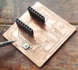
 At the end of the group work with comrade Ronal, with the card printed after the scarving.
Setting up the circuit
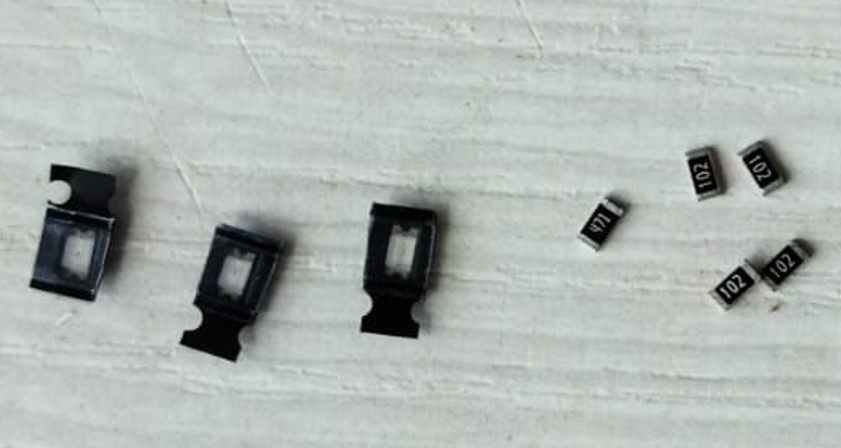
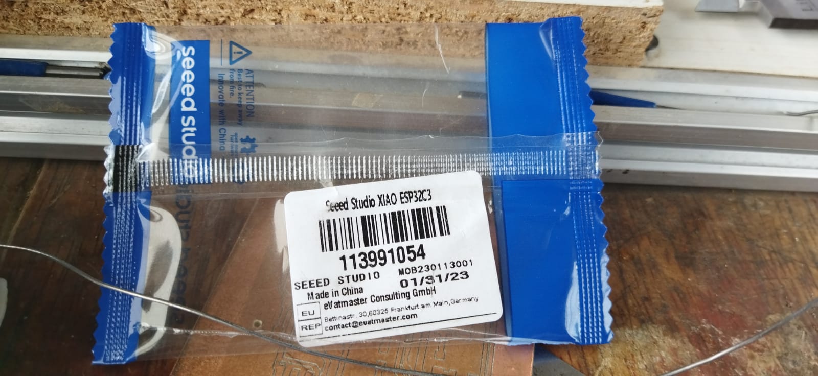 It’s time to assemble the circuit with the electronic components: as we can see we have the LEDs and resistors ready according to their values that were ordered, in addition the XIOAO microcontroller ESP32C3 just taken out of its bag.
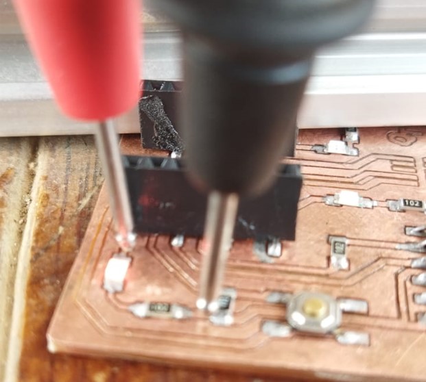
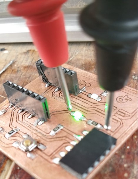
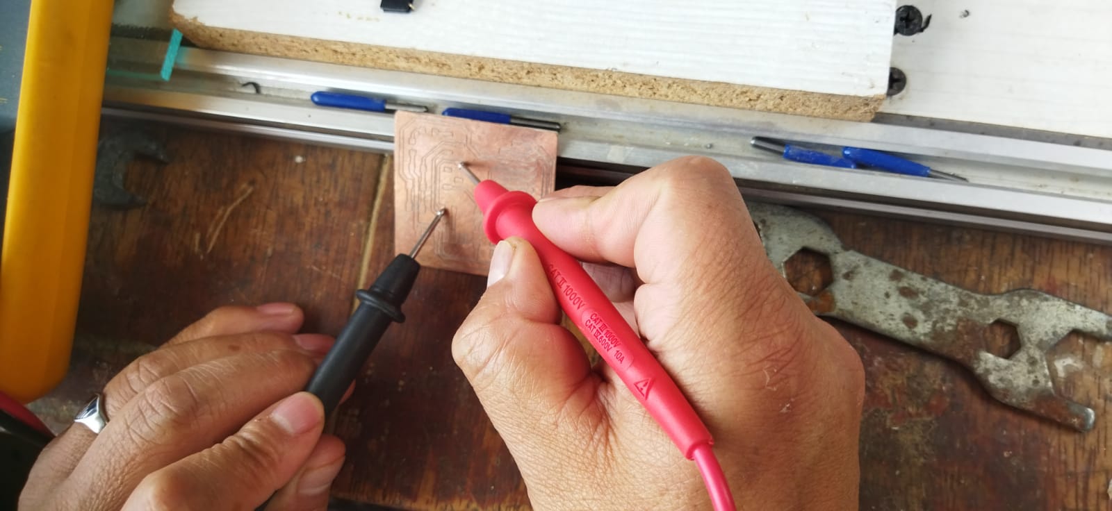 Doing Continuity Testing with the Multimeter
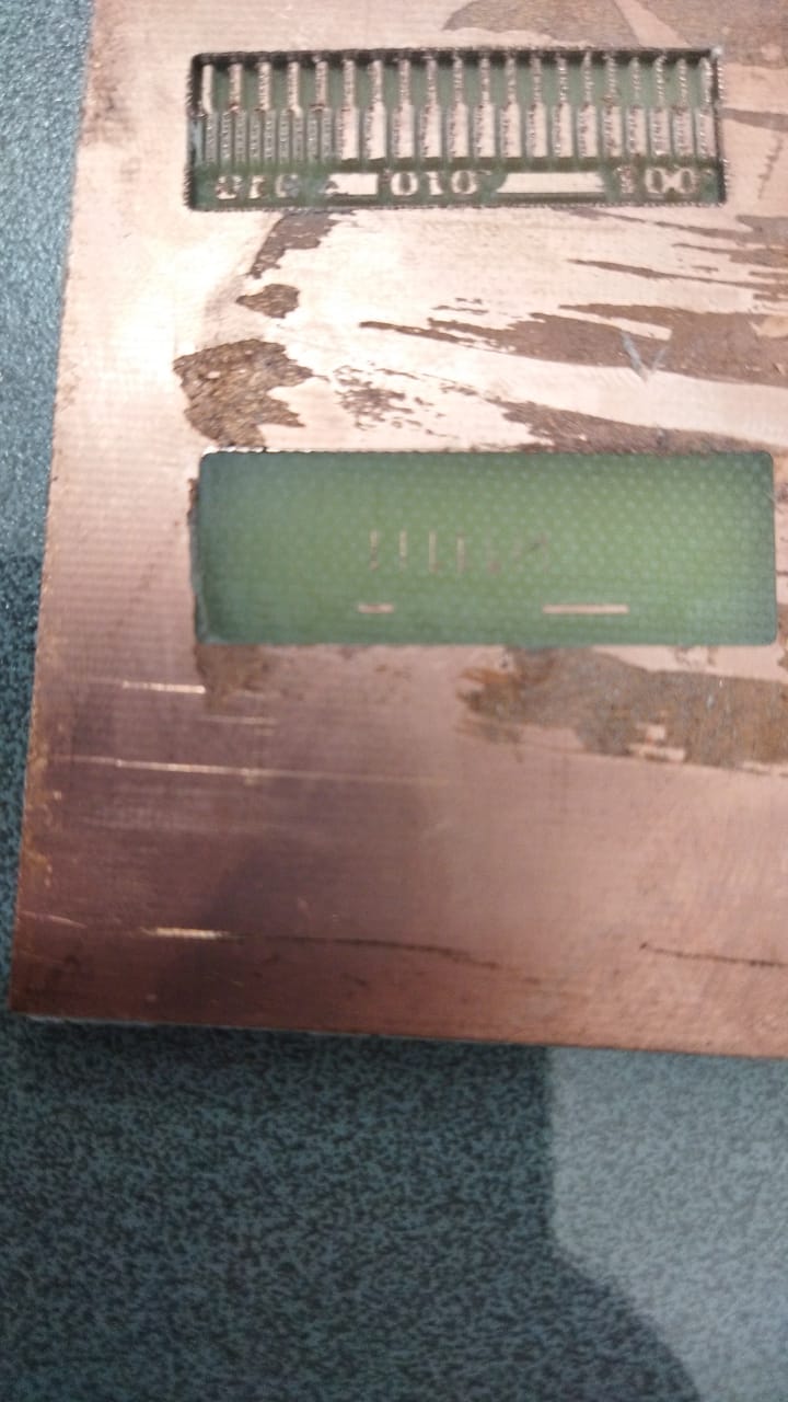
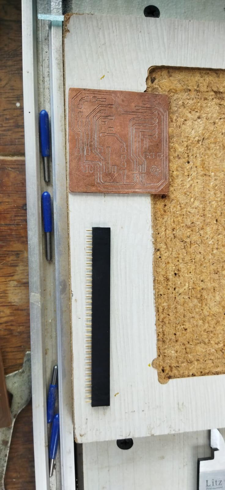 The Printed Circuit Board and the Connector Strip Outwards.
Passing flux and tin to the connection points that we will have to solder in the circuit.
The Printed Circuit Board and the Connector Strip Outwards.
Passing flux and tin to the connection points that we will have to solder in the circuit.
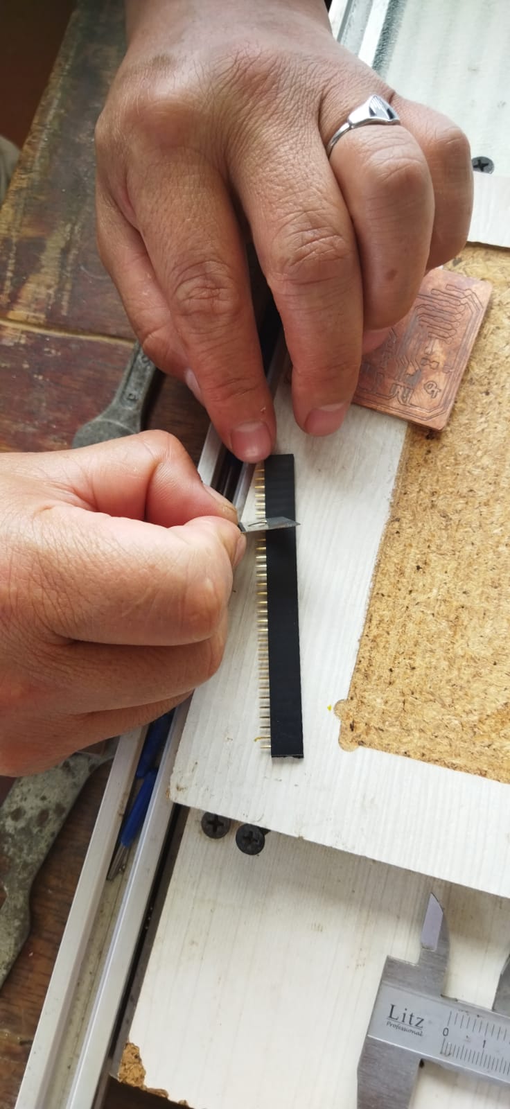 Making the Connectivity Strip Cuts
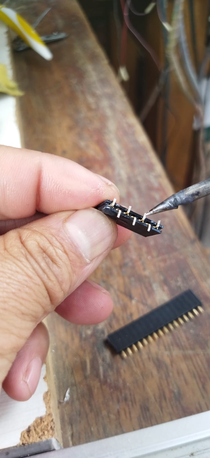 After the cuts, flux and tin were passed in the terminals
 Ready to be soldered onto the board to connect to the XIAO microcontroller

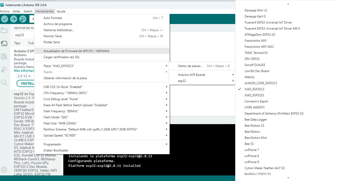
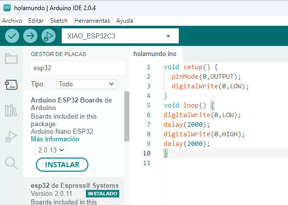
 Steps to perform for configuration on the computer with the arduino
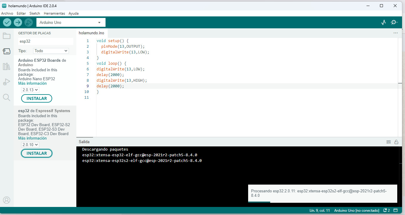


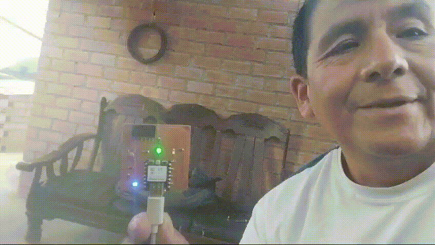
At the end, it was possible to connect and achieve the flickering of the light according to the programming in the arduino
===================================================================
# sumary
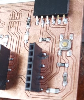
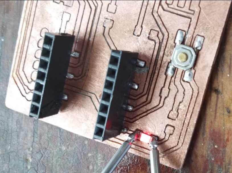
In this task I have experienced knowing that when a component is crossed it can show proving continuity that something is crossed, I spent almost an hour seeing where the junction was, my colleague suggested me to desolder the LED diode that was near the crossing mark and surprise the crossing was corrected, we changed the component and the card stopped marking crossover.
And as proof of error, I show the crossover component.

Results: Electronics Production
After the entire process of manufacturing a printed circuit board, here is the result of Quentorres PCB.
For it to work in the programming world hello world I need to use this code in Arduino IDE.
const int ledPin =  D0;      // the number of the LED pin
const int buttonPin = D1;     // the number of the pushbutton pin
int buttonState = 0;         // variable for reading the pushbutton status

void setup()
{
  Serial.begin(9600);
  pinMode(buttonPin, INPUT);
  pinMode(ledPin, OUTPUT);
}

void loop()
{
  buttonState = digitalRead(buttonPin);
  if (buttonState == HIGH) {

    for (int i=0; i <= 10; i++)
      {
        delay(100);
        digitalWrite(ledPin, HIGH);
        delay(100);
        digitalWrite(ledPin, LOW);
      }
  } else {

    digitalWrite(ledPin, LOW);
  }
  }