9. Embedded programming
This week assigment is to read the datasheet of the chip used: I have used ATtiny 45 and to use the produced programmer in electronic production to program the HelloWord PCB produced in electonic design assignment.
Research
ATtiny 45 features:
-
2/4/8 K byte of In-System Programmable Flash
-
128/256/512 bytes of EEPROM, 128/256/256 bytes SRAM.
-
6 general purpose I/O lines, 32 general purpose working registers, one 8-bit high Timer/Counter, Universal Serial Interface.; Internal and External Interrrupts.
-
A 4-channel, 10-bit DC. A programmable watchdog Timer with internal oscillator, and 3 software selectable power saving modes.
-
The idle mode stops the CPU while allowing the SRAM, Timet/Counter, and interrupt system to continue functionning; The power-down mode saves the register contents, disabling all chip functions until the next interrupt or hardware reset.
-
The ADC noice reduction mode, stops the CPU and I/O modules except ADC, to minimize suitching noise during ADC conversions. The device is manifactured using Atmel’s high density non-volatile memory technology.
-
The on-chip ISP Flash allows the program memory to be re-programmed in system on SPI serial interface; by a conventional non-volatile memory or by an on chip boot code running on the AVR core.
-
The ATtiny 25/45/85 AVR is is supported with a full suite of program and system development tools including: C Compilers, Macro Assemblers, Program Debugger,Simulators, In-Circuit Emulators and Evaluation Kits.
ATtiny 45 pin description:
-
VCC: Suply Voltage
-
GND: Ground
-
Port B(PB5…PB0): Port B is 6-Bi-directional I/O port with internal pull-up resistors(selected for each bit).
The port output buffers have symmetrical drive characteristics with both high sink and source capability.
As inputs, Port B pins that are externally pulled low with source current if the pull-up resistors are activated.
- Reset: Rest input, a low level on this pin for longer than the minimum pulse length will generate a rest, even if the clock is not running.
Programming the produced PCB
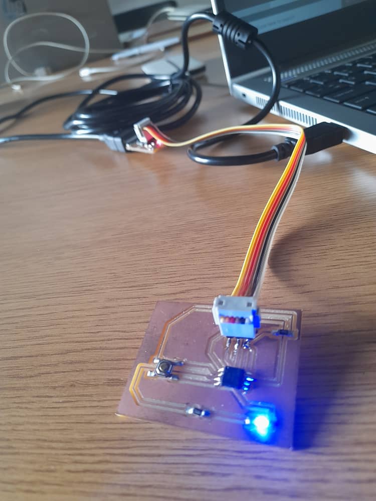
To program my designed and produced PCB, I need to have a programmer and here I have to use the produced programmer in electronics production assignment.
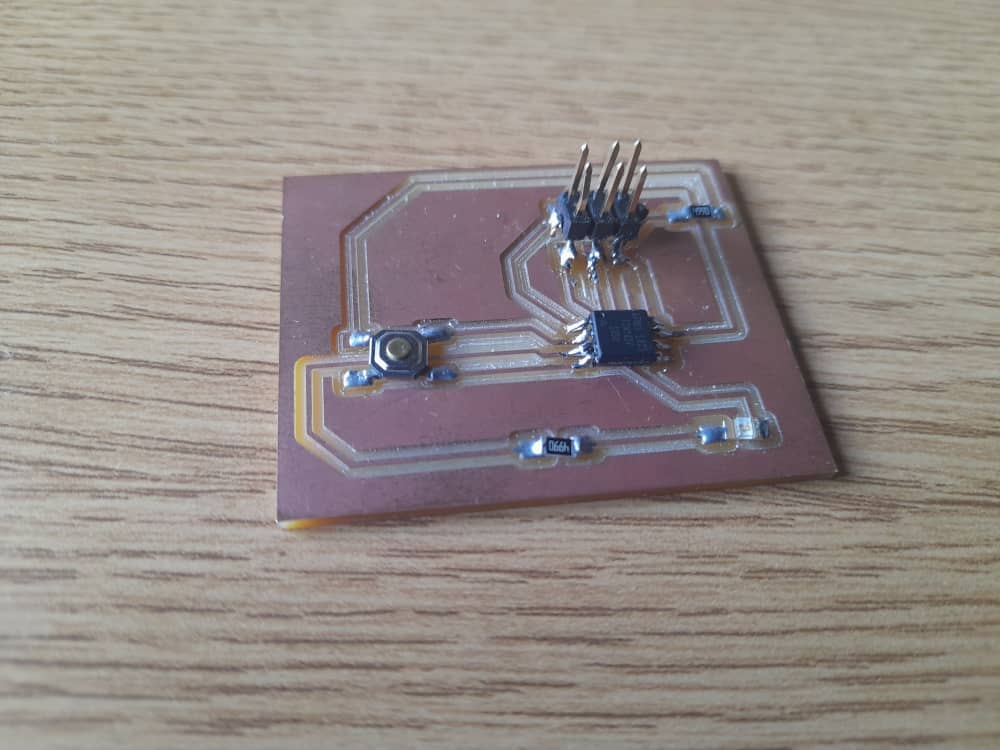
Below, is my HelloWorld PCB created in electronic design to program so that its LED can be On.
Below, is the programmer to use which is the In-Circuit Programmer produced in electonic production assignment.

Steps to program my board
I first dawnloded arduino software here because I need arduino IDE to program my board and below is the interface of arduino when you open it.

I have followed this tutorial to program my board and the following are steps used:
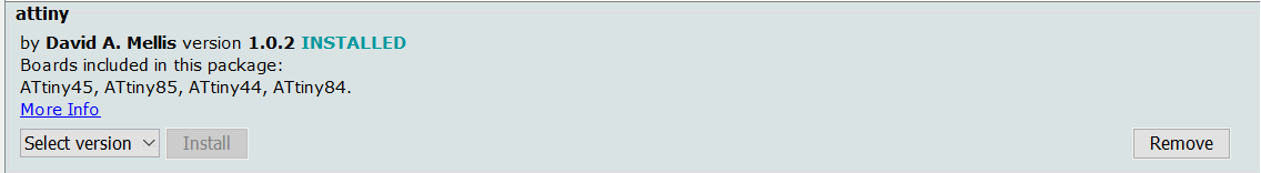
First I have to add ATtiny 45 library in arduino IDE by Opening arduino and go to File–>Preference On the Preferences windows, on the Additional Boards Manager URLs section I pasted the followed link https://raw.githubusercontent.com/damellis/attiny/ide-1.6.x-boards manager/package_damellis_attiny_index.json then click 0k as shown by the red color on the image below.

Go to Tools–>Board–>Boards Manager here I installed one of David A.Mellis as you can see below

Below, as you can see the library is installed
Go to Tools–> Board–> Select your library(if your library was installed correctly you will find it) then choose your chip.

Select Tools–> Chip–>Select the exact chip of your board(for me it is ATtiny 45) as you can see below

Go to Tools–>Clock Source–>1MHZ(Internal)
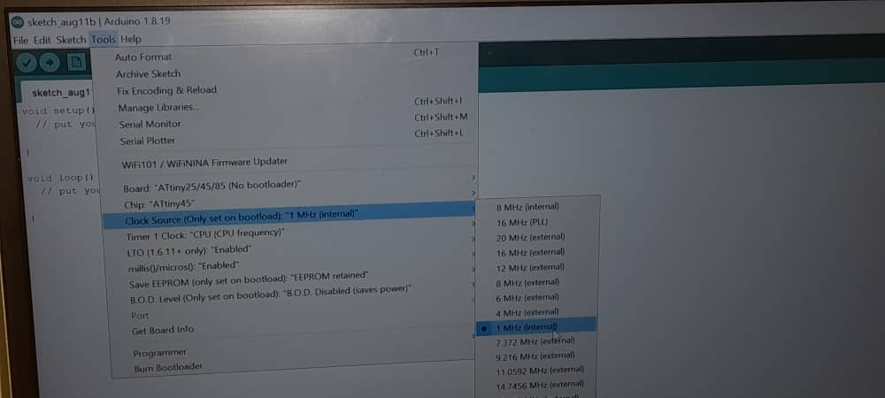
Select Tools–>Programmer–>USBtinyISP

I have used the following ATtiny 45 pinout in order to connect my LED and Switch on ATtiny 45.

Now, It’s time to run arduino code to blink the LED on the board, to do it double check if you have selected a correct board, chip, programmer, and port then compile, when you found that there is no eroors in your code, the last step is to upload your code into the produced board.
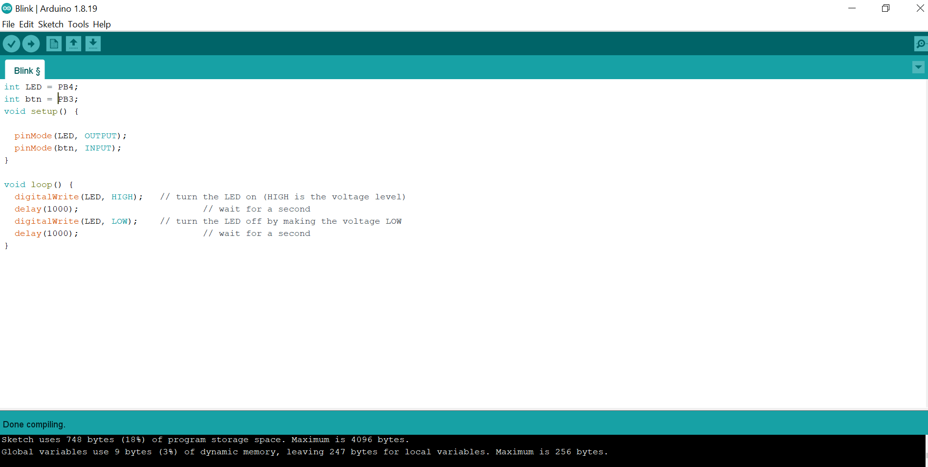
Code used, you can copy and reuse them, the only thing you have to change are pins initialization according to where your LED or button are connected with your chip.
int LED = PB4;
int btn = PB3;
void setup() {

  pinMode(LED, OUTPUT);
  pinMode(btn, INPUT);
}

void loop() {
  digitalWrite(LED, HIGH);   // turn the LED on (HIGH is the voltage level)
  delay(1000);                       // wait for a second
  digitalWrite(LED, LOW);    // turn the LED off by making the voltage LOW
  delay(1000);                       // wait for a second
}
After programming my HelloWorld its LED lighthened.
Files Used Here
GROUP ASSIGNMENT
The group assignment was to compare performance and development workflows for other architectures
Research
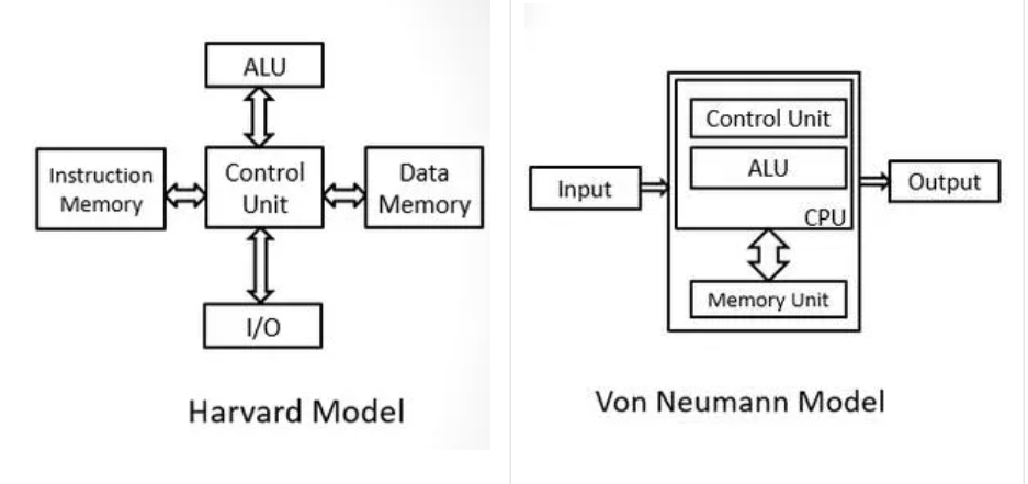
To carry out our assignment we first search for what is architecture of a micro-controller and we found that it refers to the arrangement of the CPU with respect of the RAM and ROM; How microcontroller is structured internally.
All microcontrollers use one of two basic design models(Harvard architecture and Von-Newmann archictecture, they represent two ways of exchanging data between CPU and memory). Microcontrollers with Harvard archictecture are called RISC microcontrollers and others with Von-Newmann’s architecture are CISC microcontrollers.
Microcontroller is used inside an embedded system for managing the function of devices. Embedded System is centered arround its microcontroller unit(MCU). It may help you to select the right microcontroller for your embedded systems solution which may lesd to the success or failure of your system.
The used chip, which is ATtiny 45 is in RISC(Harvard architecture).
Comparison between Harvard architecture and Von-Newmann’s architecture
- In Harvard architecture, the CPU is connected with both the data memory(RAM)and Program memory(ROM)separately, whereas In Von-Newmann’s architecture, there is no separation between data and program memory; Instead a single memory connection is given to the CPU.
-
Harvard architecture requires more hardware since it will be requiring separate data and address bus for each memory,in contrast Von-Newmann’s architecture requires less hardware since only a common memory needs to be reached.
-
Harvard architecture requires more space, while Von-Newmann’s architecture requires less space.
-
In Harvard architecture, speed of execution is faster because the processor fetches data and intructions simultaneousily, whereas in Von-Newmann’s architecture speed of execution is slower since it can not fetch the data and instructions at the same time.
-
Harvard architecture results in wastage of space since if the space is left in the data memory then the instructions memory can not use the space of the data memory and vice versa, as opposed to Von-Newmann’s architecture where space is not wasted because the space of the data memory can be utilized by instructions memory and vice versa.
-
In Harvard architecture controlling becomes complex since data and intructions are to be fetched simultaneousily, while in Von-Newmann’s architecture controlling becomes simpler since either data or instructions are to be fetched at time.