5. Electronics production
This week I worked on electronics production.
Group Assignment
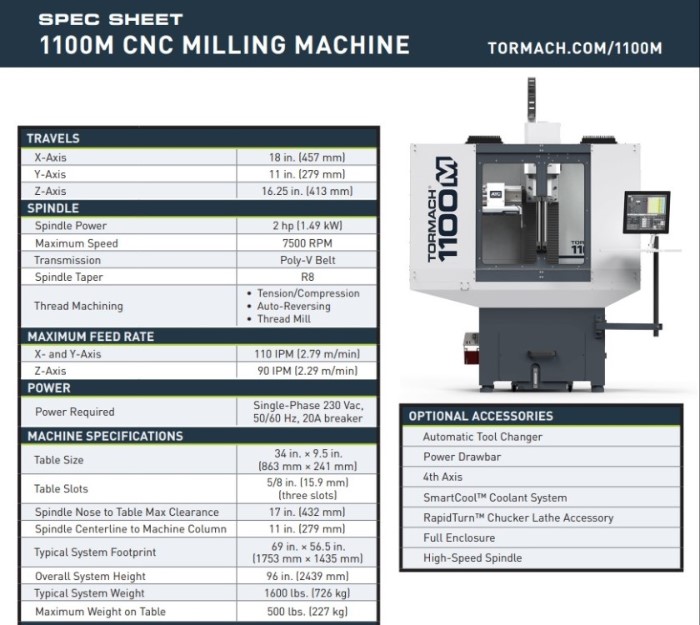
In the lab we have a Tormach 1100M Milling Machine
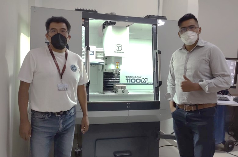 It can cut challenging materials like titanium, aluminum, wood, or plastics, but also it can fabricate delicate works as PCB milling.
These are the main specifications:
It can cut challenging materials like titanium, aluminum, wood, or plastics, but also it can fabricate delicate works as PCB milling.
These are the main specifications:
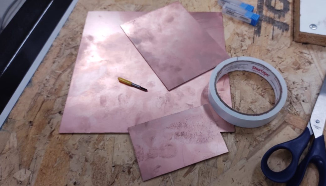
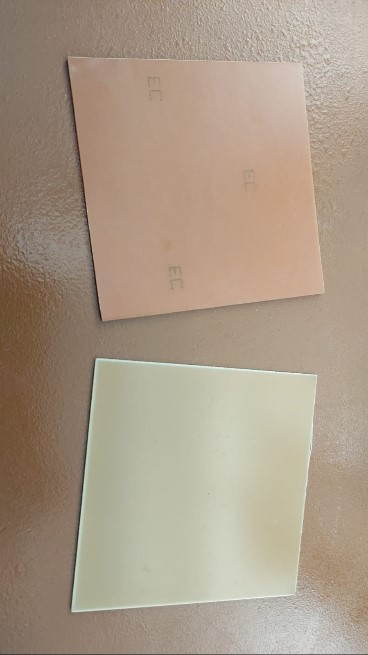
 For the assignment we had the 60 degree V bit, the copper clad board of 1.2 mm thick (bakelite and fiberglass) one side and double contact tape.
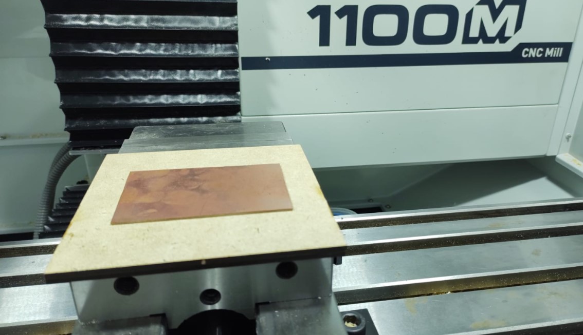
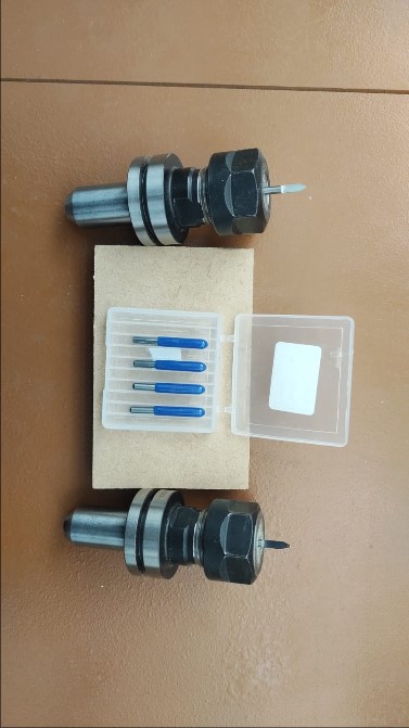
The bits available in the FabLab are 1/64” (approx. 0.39mm) for the strokes and another 1/32” (approx. 0.79mm) for the outline.
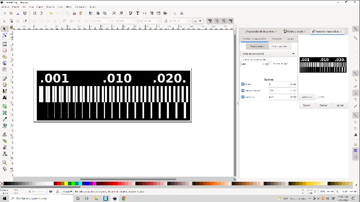
For test templates, we use the file available at The Fab Academy 2022 Schedule. This format is in .png
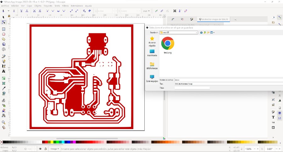
We need to convert the .png templates to a milling pattern. So we used Inkscape
to vectorize the image. Select and place vectorize by luminosity. Then we save the file in .SVG format.
With this file we create the milling pattern in jscut. First we load the .SVG file select it and create the operation “pocked” 0.2 mm. We load the characteristics of the 0.39 mm diameter tool.
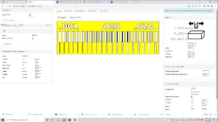
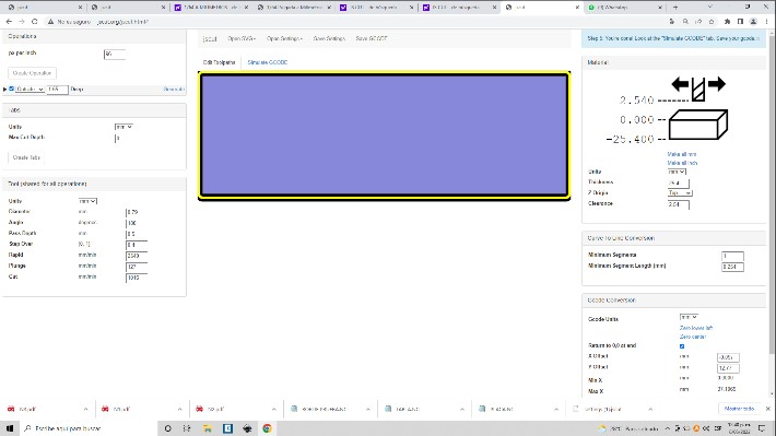
The same procedure is followed for the cutting edge changing the diameter of the tool to 0.79 mm We save the Gcode in .nc format.
Router Setup and Template Run:
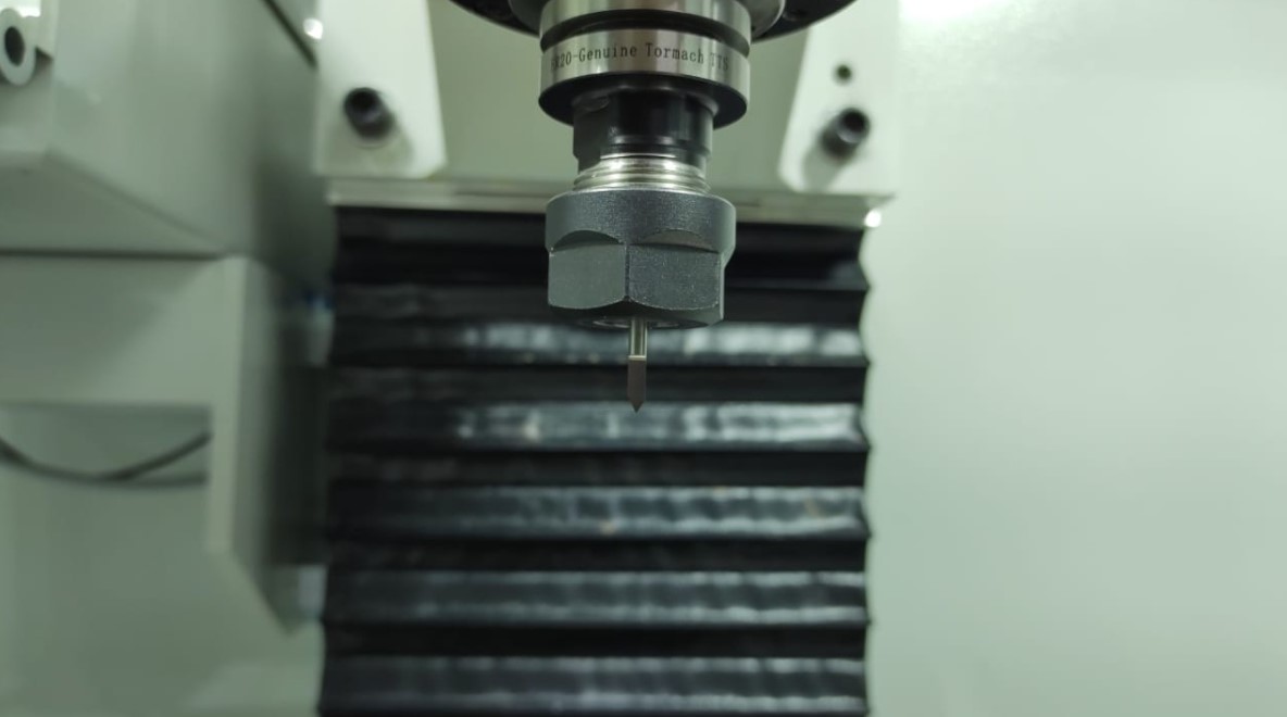
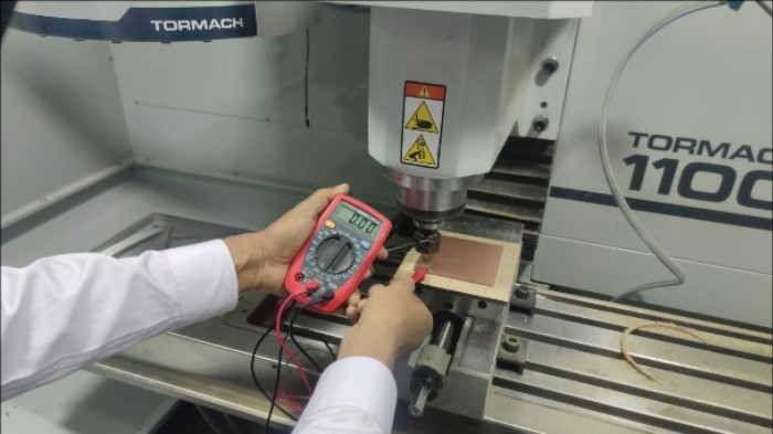
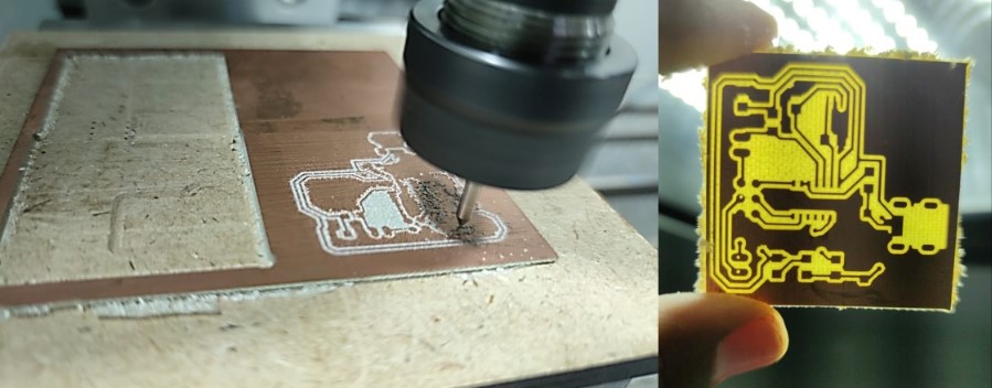
Before we send the file to the mill, we need to calibrate the X and Y axis. Bottom left to start the job. The most important is the Z axis. For this we use a multimeter to align the copper plate with the tip of the cutter.
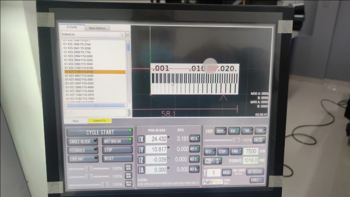
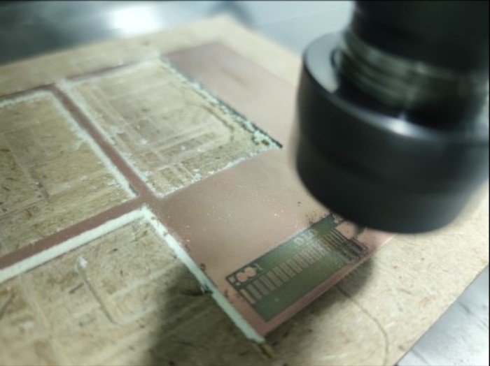
Finished this process the cut of the edge of the template is executed. For this the cutter is changed to 1/32”.
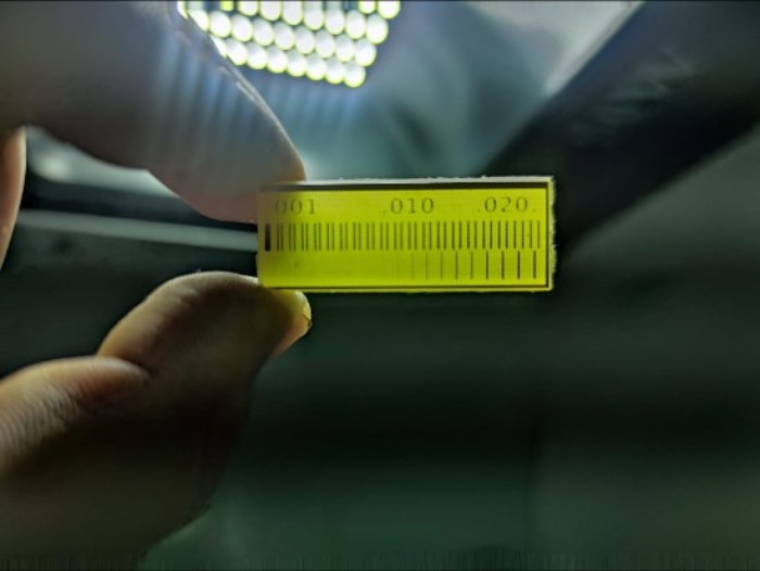
According to the result of the milling of the template we can conclude that the traces to make circuits have to be equal to or greater than 0.015” or 0.39mm
Individual Assignment
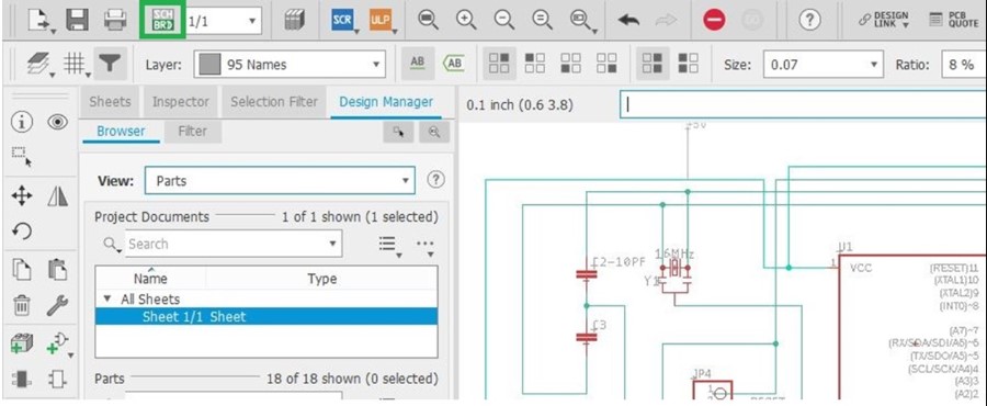
To Make an in-circuit programmer that includes a microcontroller, Eagle software version 9.6.2 was used. This program is used for the design of electronic circuits and the respective development of the PCB schematic as it provides a large variety of electronic component libraries that can be added as the process develops.
After opening the program, a new file has to be opened. In this case, you started with the design of the circuit schematic, so you have to follow the following sequence.
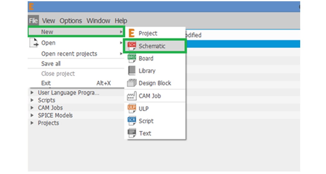
With this you have to open the work window in order to be able to start with the schematic diagram of the circuit.
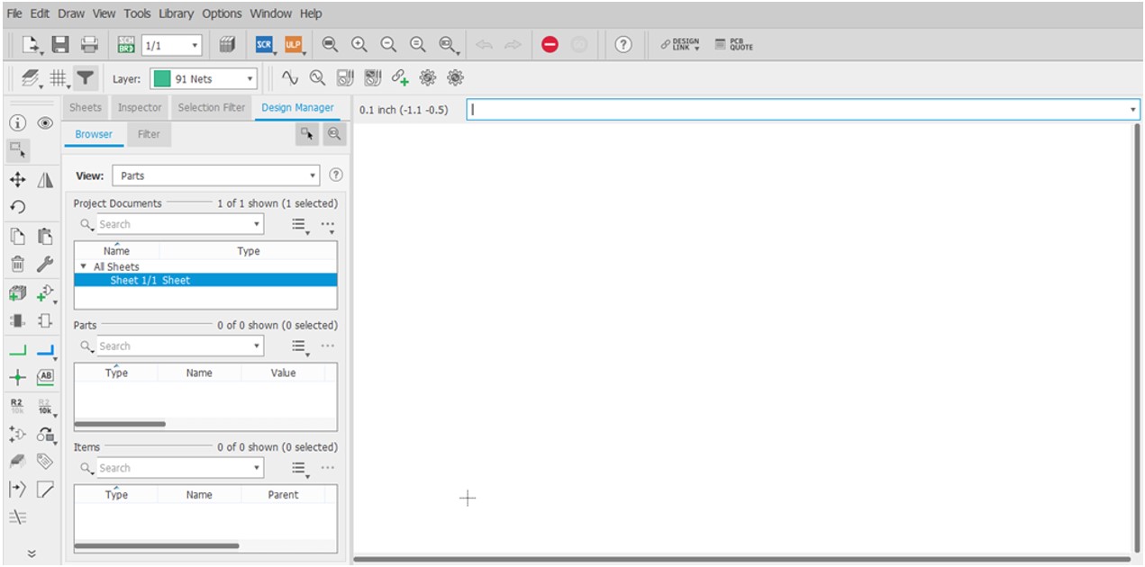
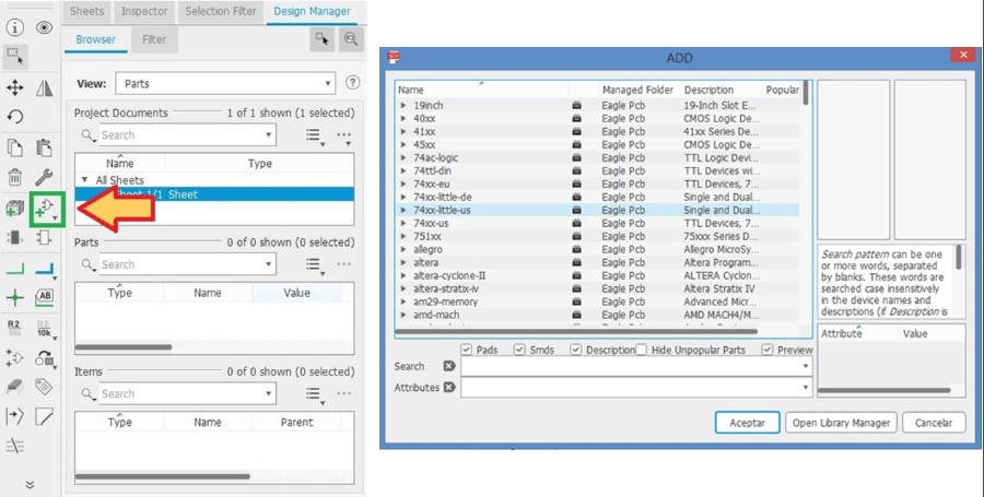
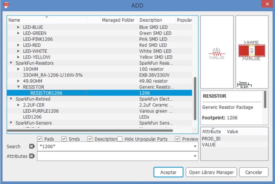
To add the electronic components in the work area, select the option “Add Part” from the toolbar and the following window will open where all the electronic components are available. To search for them, type the technical name of the required component in the “Search” bar.
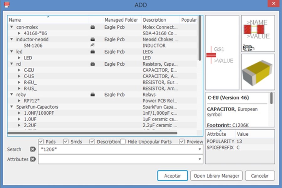
 For a more precise search, it is recommended to enter the technical name or the component code as shown below. In this example, it is required to search for capacitors and resistors with SMD characteristics and for this purpose 1206 is entered, as this is the code of these components in the Eagle libraries.
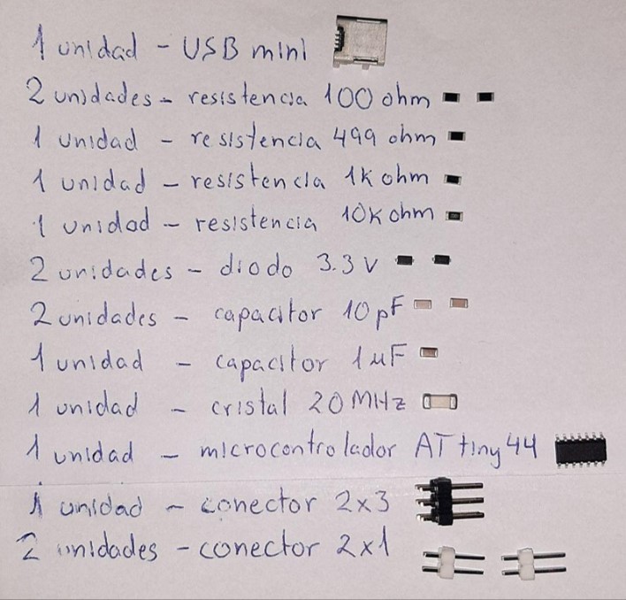
 For the schematic circuit of the programmer the following components have to be used.
- 01 ATtiny44 microcontroller.
- 01 1 kΩ resistor.
- 01 499 Ω resistor.
- 02 100 Ω resistors.
- 01 10 kΩ resistor.
- 02 10 pF capacitors.
- 01 1 uF capacitor.
- 02 3.3 V diodes.
- 01 20 MHz crystal.
- 01 Mini USB connector.
- 2x3x2x3 sprats
For the schematic circuit of the programmer the following components have to be used.
- 01 ATtiny44 microcontroller.
- 01 1 kΩ resistor.
- 01 499 Ω resistor.
- 02 100 Ω resistors.
- 01 10 kΩ resistor.
- 02 10 pF capacitors.
- 01 1 uF capacitor.
- 02 3.3 V diodes.
- 01 20 MHz crystal.
- 01 Mini USB connector.
- 2x3x2x3 sprats
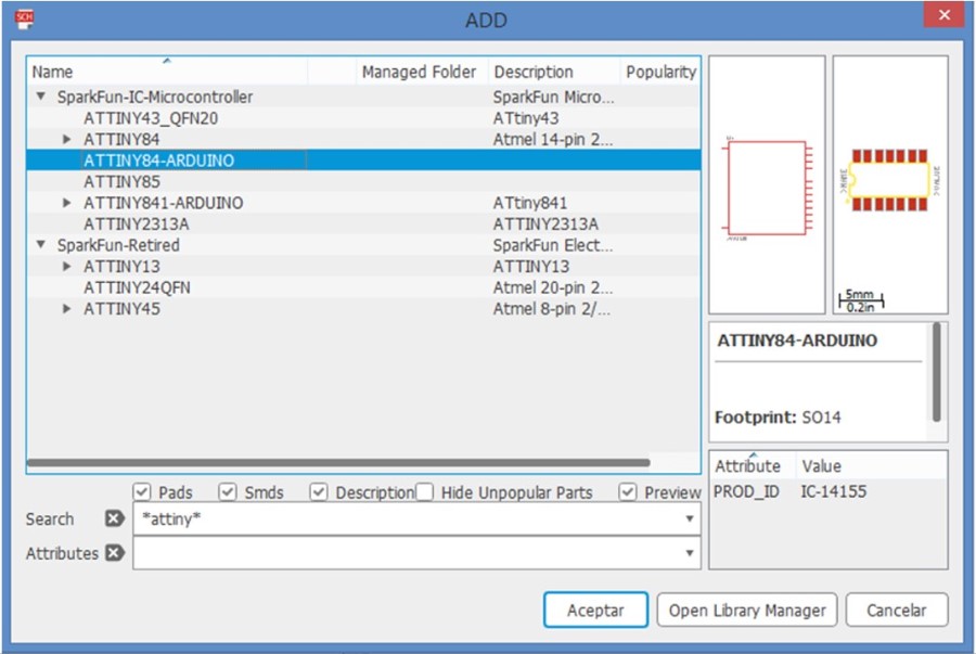
The following shows the search process for the ATtiny44 microcontroller. This component is shown in the “Sparkfun-IC-Microcontroller” library under the name “ATTINY84-ARDUINO”. Select the component and click on “OK”.
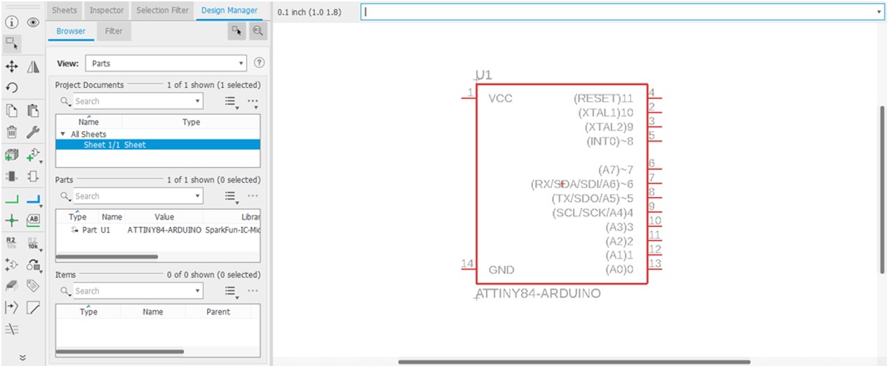
Then place it in the work area. With the “Esc” key you can return to the component search window to add the next component.
The next components to be added are SMD resistors and capacitors. These are searched for in the Eagle libraries:
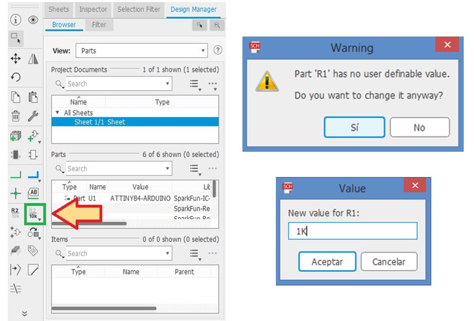
In order to give a value to the resistor you have to go to the toolbar and select the “Value” option. Then select the resistor to which you want to add a value and accept it instead. Then place the value of the resistor in the next window and accept it.
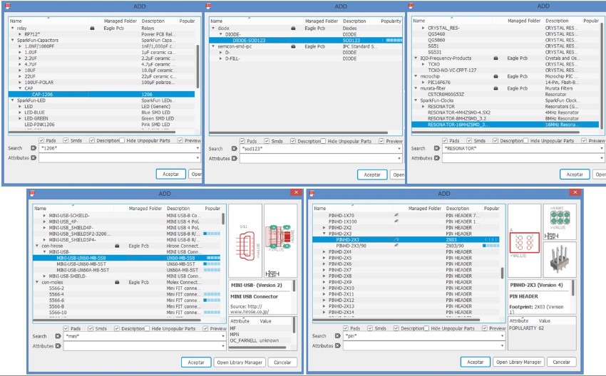
In the case of the capacitors, the 3.3 V diodes, the 20 Mhz crystal, the USB connector and the springs are chosen from the library as shown in the picture:
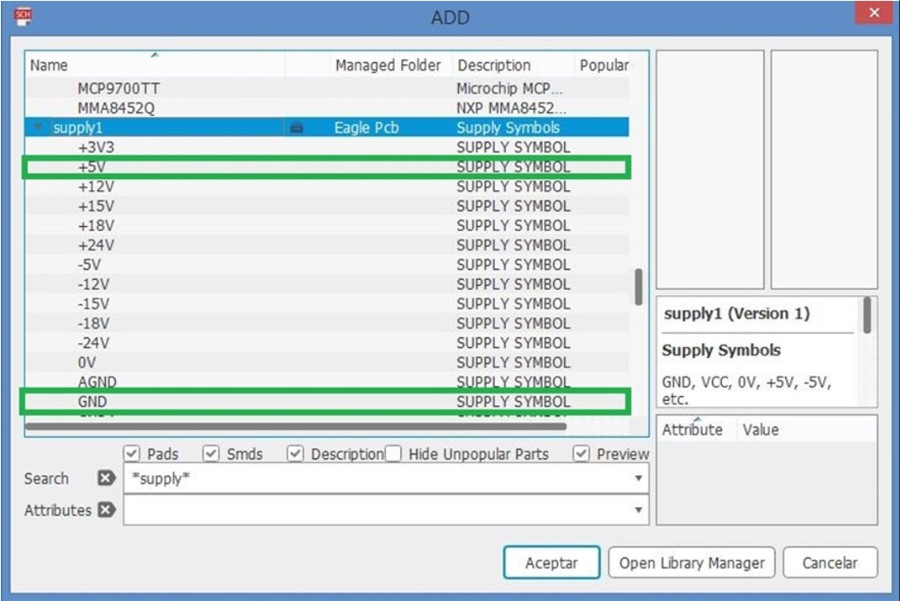
In order to add the 5 V signal and the GND signal to the schematic diagram of the circuit you have to select the “Supply1” library and select the components shown below.
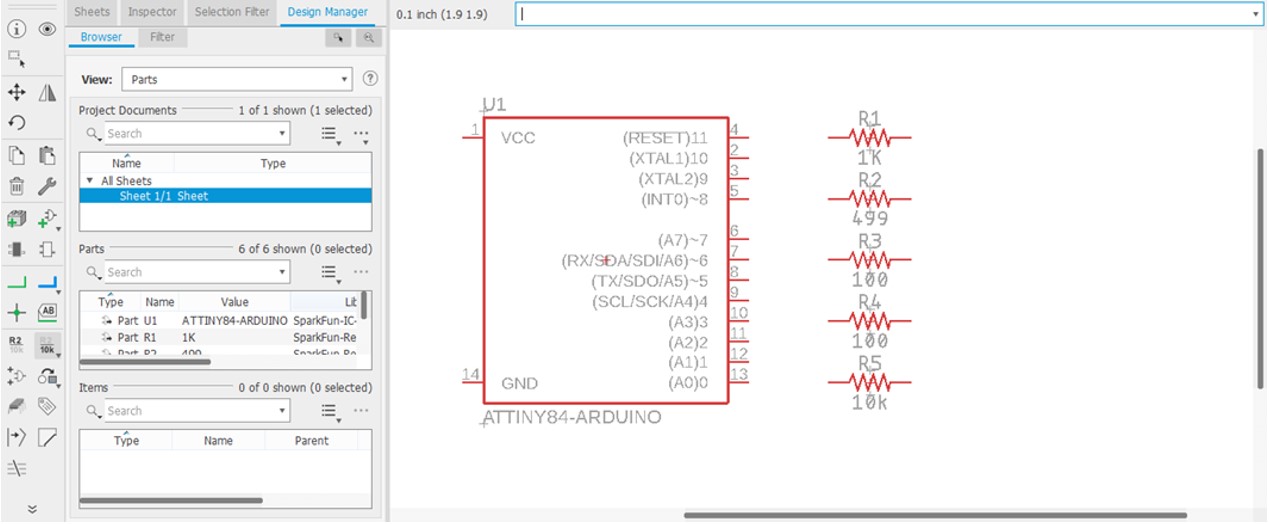
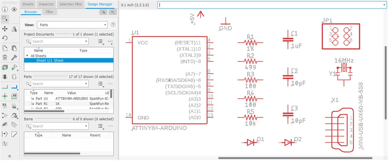
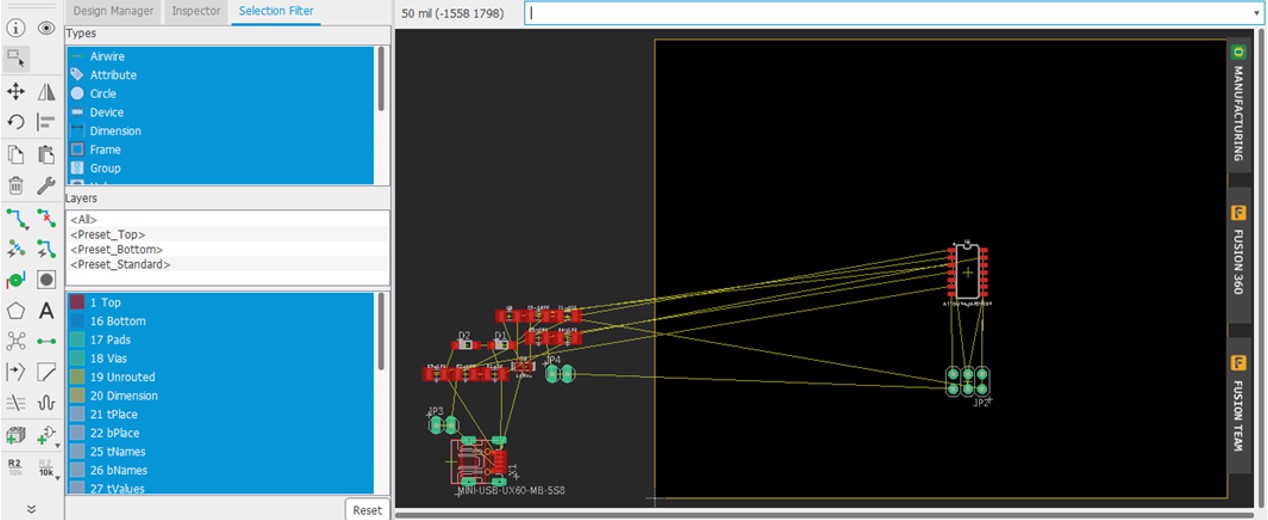
In the work area you should have all the components shown below.
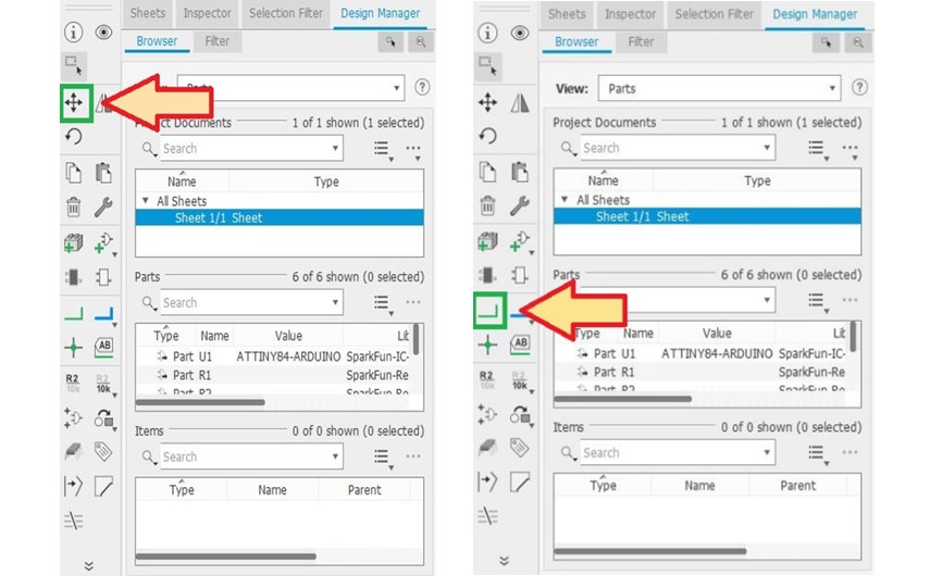
It is recommended to arrange all components in such a way that the schematic circuit diagram is as organised as possible by using the “Move” tool in the toolbar. The “Net” tool is used to join the components.
After the components have been attached to the work area, the schematic should look like this.
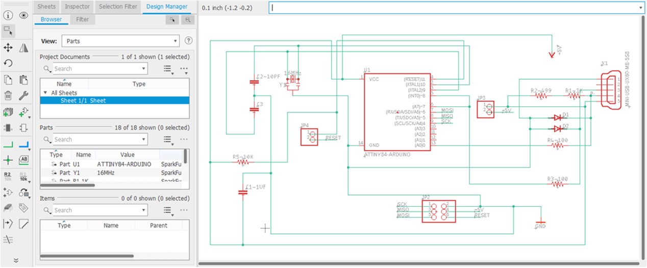
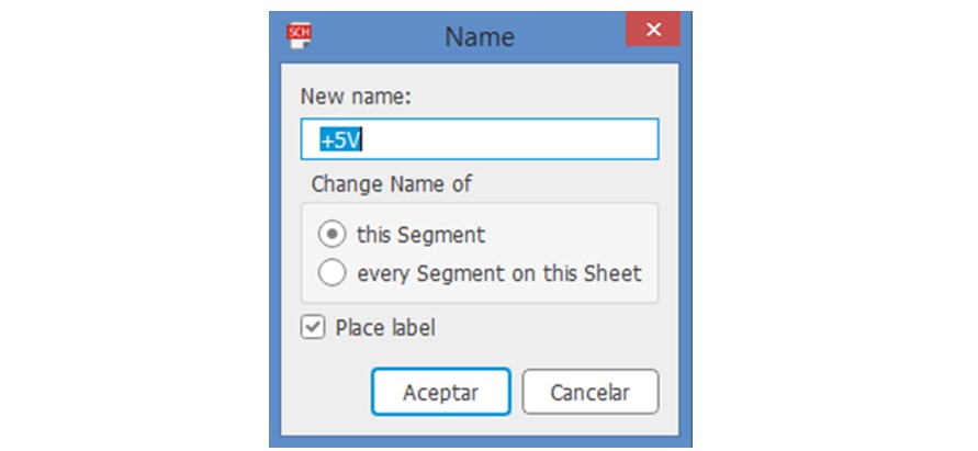
To change the names of the signals and thus reduce the number of connections, right click on the connection whose name you want to change and select the “Name” tool and the following window for changing the name will appear.
To create the PCB design, go to the “Generate/switch to board” option:
The components must be moved to the black box and can also be rotated to make the design more orderly. The components must be positioned in the way you want the board to look physically.
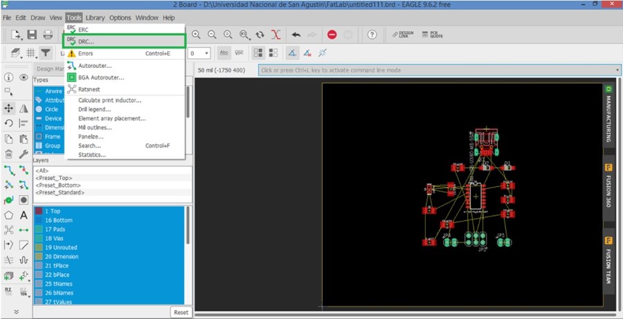
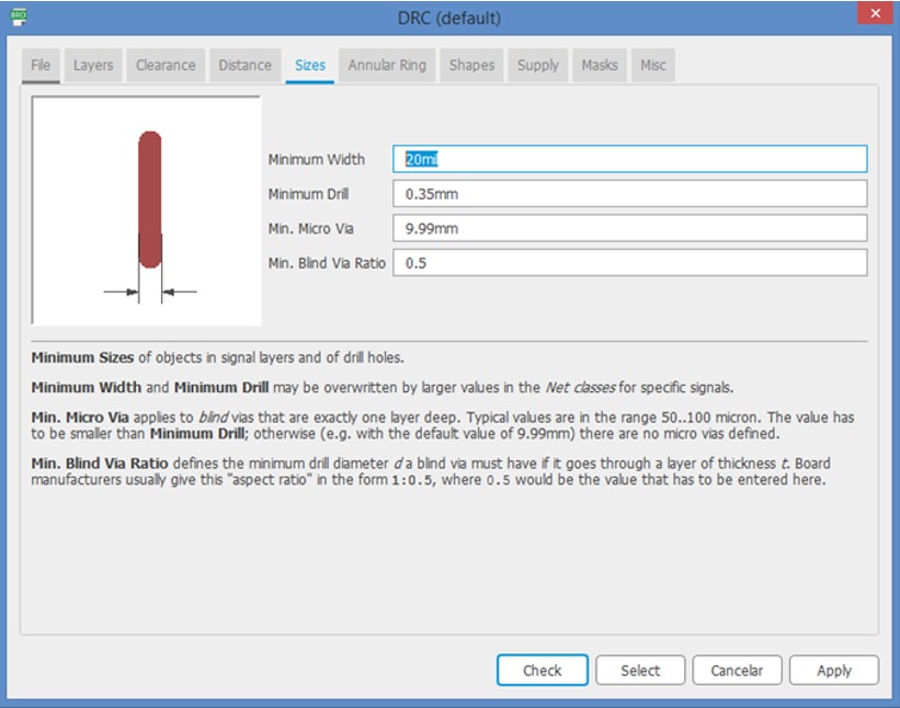
In order for the Tormach CNC to mill the tracks correctly, some track parameters have to be configured as shown below. To do this, go to “Tools” and then “DRC”.
The following window will appear and in the option “Sizes” you have to configure the option “Minimum Width” so that the tracks have a thickness of “20mil” and the milling machine does not have errors at the moment of carrying out the process.
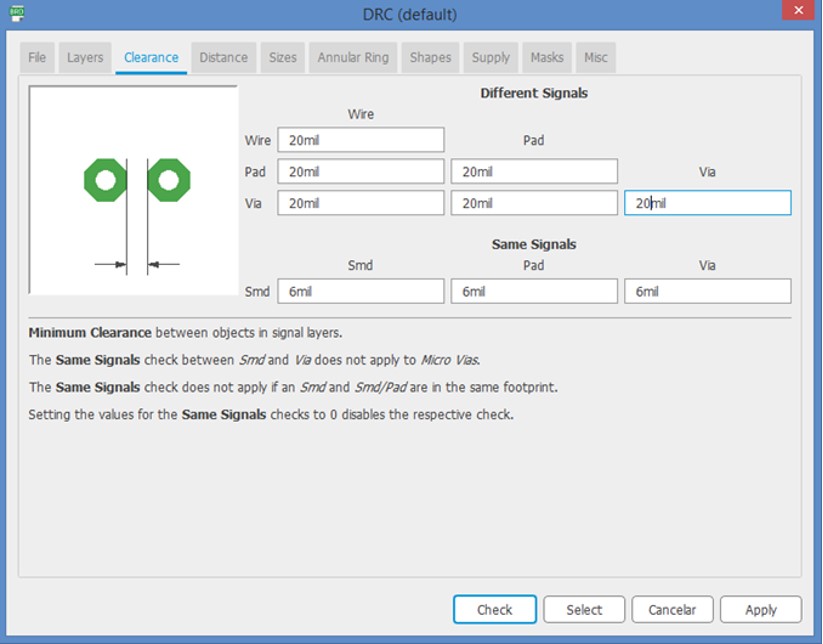
Then we go to the “Clearance” option and modify the following parameters as shown below. Then click on “Apply”.
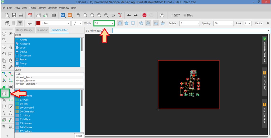
To make the rest of the board GND we create a “Polygon” and give it a thickness of 20 as shown below:
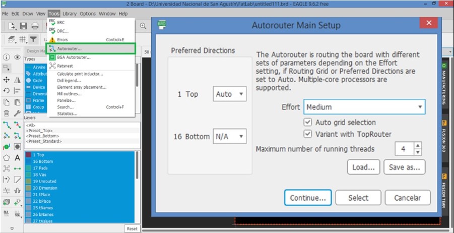
To generate the tracks you will use the “Autorouter” tool, this tool allows you to automatically generate the tracks of the board, this tool can also be found in the “Tools” option. In this window you can configure the type of effort that the programme makes to automatically generate the tracks, in this case you can set the effort to “Medium”. The “Top” option must be set to automatic, while the “Bottom” option must be set to N/A.
It is recommended to use the “Ratsnest” option so that the GND appears correctly on the board layout.
You can configure the tracks made automatically, i.e. you can change the position and thickness of these tracks to get a better finish of the board. As you can see some tracks were not made automatically, these tracks have to be made manually, as an option you can make use of bridges that also have to be configured using Eagle.
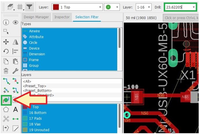
In order to make a bridge, the tool “Via” has to be used, in the option “Drill” the size of the bridge terminal can be selected.
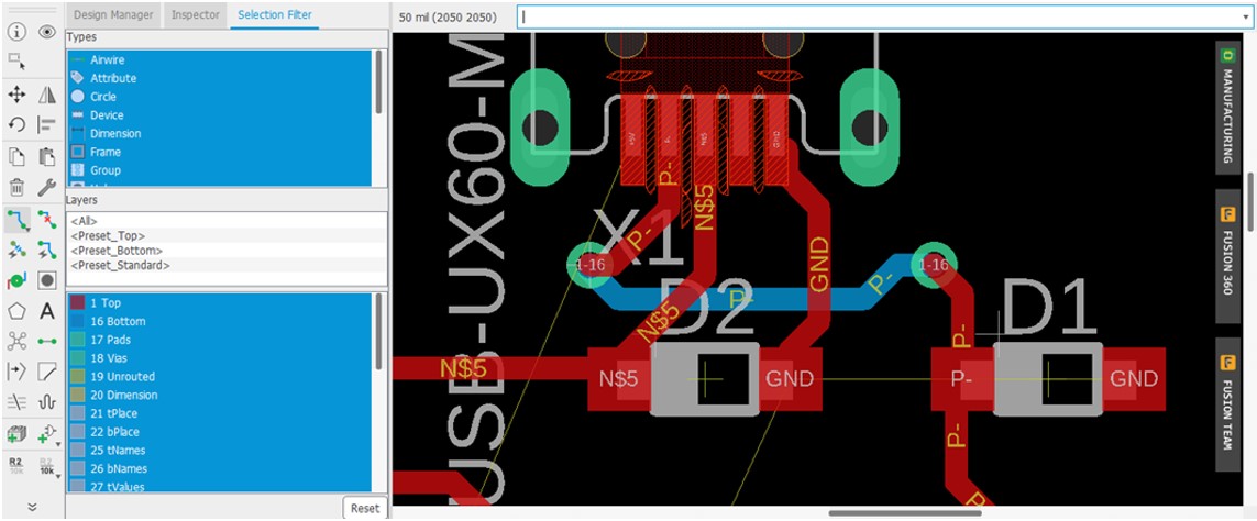
To make the bridge, select the “Route Airwire” option (this tool is used to make the tracks). Select where you want to make the bridge (this action must be done in the “Top” layer), then switch to the “Bottom” layer and the previously selected route appears automatically and the blue track is formed as shown below. To finish the bridge you have to go back to the “Top” layer and the track appears automatically to finish the bridge.
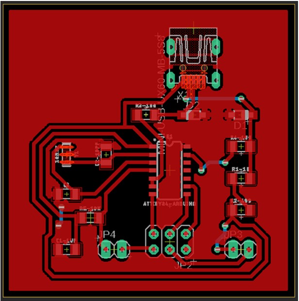
After having finished the bridges, the plate looks like this and can be exported as an image file.
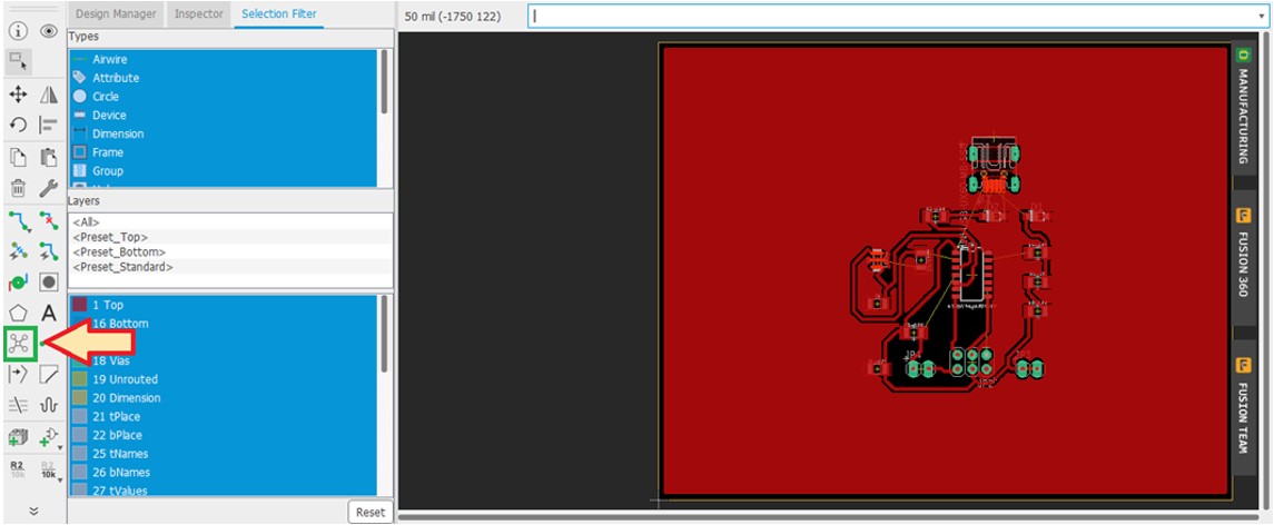
To export the file, only the layers “Top”, “Pads” and “Roads” have to be left visible.
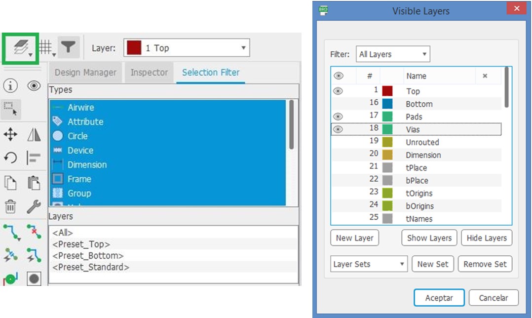
To export the file as an image, click on “File”, then on “Export” and finally on “Image”. In the pop-up window, choose the “Resolution” of 600 dpi and activate the option “Monochrome”.
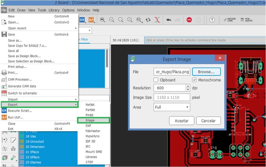
It is also necessary to be able to export a file of the plate outline, for this purpose only the “Dimension” layer is made visible and the procedure is repeated.
In order to convert the .png image to G-code, it was first necessary to use software that allows vectorising the images. For this purpose we used the free software “Inkscape” that we learned to use in the third task: Computer Aided Design.
Open the .png file and vectorise it by selecting the image and looking in the “path” menu for the option “vectorise bitmap”. Then choose on the right side the sub-option “cut by luminosity” and apply the action.
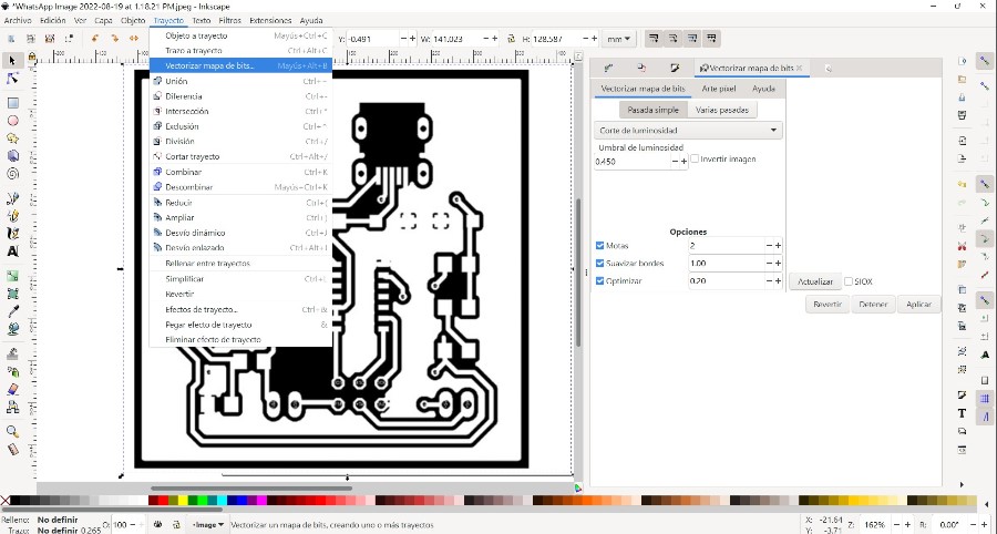 Move the image that is now superimposed with the vectors and delete it. Now you have vectors and not bits.
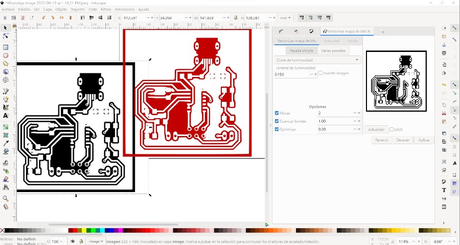 Then save it as an .svg file
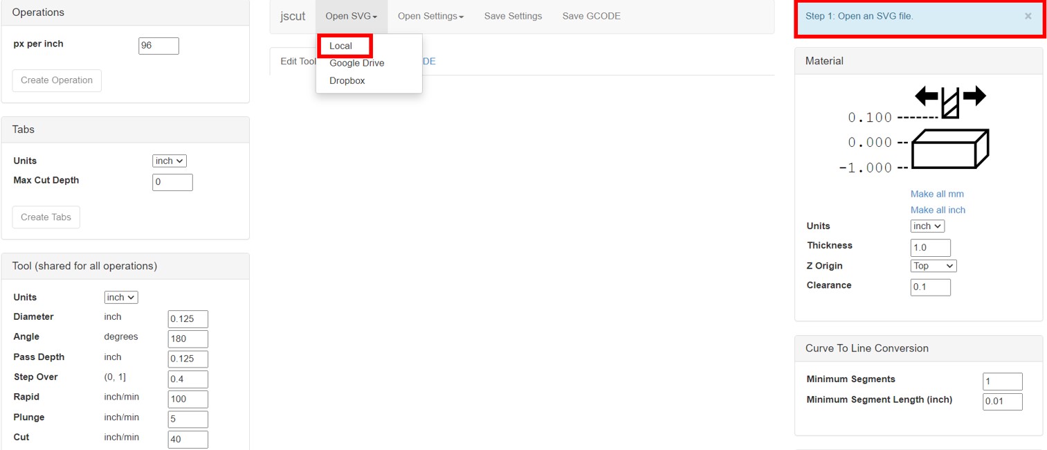
To convert this file into a G-code we chose to use a free software called jscut.Once the program is open, you have to execute 5 steps which are indicated in the upper right corner in light blue colour:
Step 1: Open a SVG file:
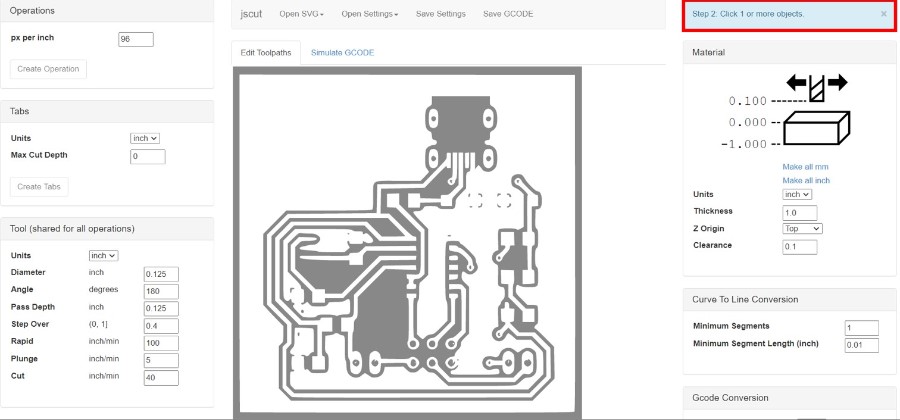
Step 2: Click 1 or more objects
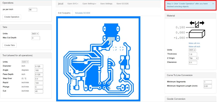
Step 3: Click “Create Operation” after you have finished selecting objects
Step 4: Click “Generate”.
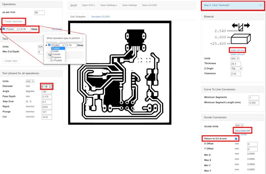 Before doing this step you need to configure:
- Make all mm
- Set the type of operation that you will develop which in our case is “pocket” with depth of 0.39
- The tool diameter: 0.39
- Zero lower left
- Return to 0.0 at end
- The other values are left as default
Step 5: You’re done! Look at the “Simulate GCODE” tab. Save your gcode.
Before doing this step you need to configure:
- Make all mm
- Set the type of operation that you will develop which in our case is “pocket” with depth of 0.39
- The tool diameter: 0.39
- Zero lower left
- Return to 0.0 at end
- The other values are left as default
Step 5: You’re done! Look at the “Simulate GCODE” tab. Save your gcode.
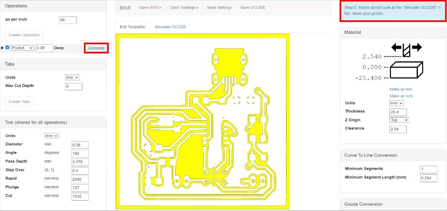 When the image turns yellow, we are done and all that remains is to see the 3D simulation and save the G-code to take it to the Tormach CNC.
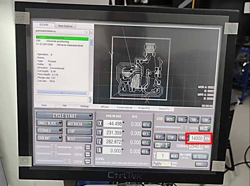
When you open the file on the Tormach CNC you only have to set the position of the coordinate origin manually and respect the RPM of 14000.
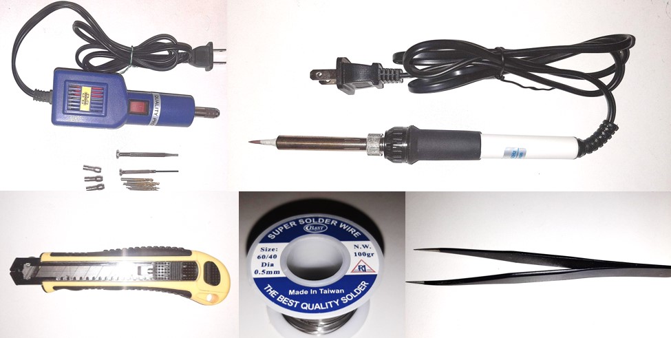
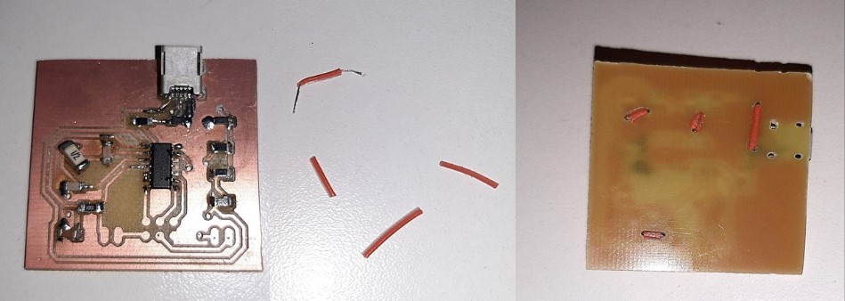
The tools used to solder the components on the board were: - PCB mini drill - Blade: - 0.5 mm tin wire - Soldering iron: - Tweezers:
The components held in the lab were as follows:
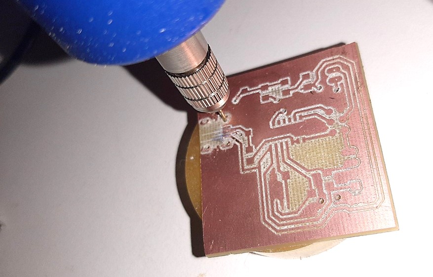
The process of soldering and finalising the board started by drilling the jumpers and the USB holes.
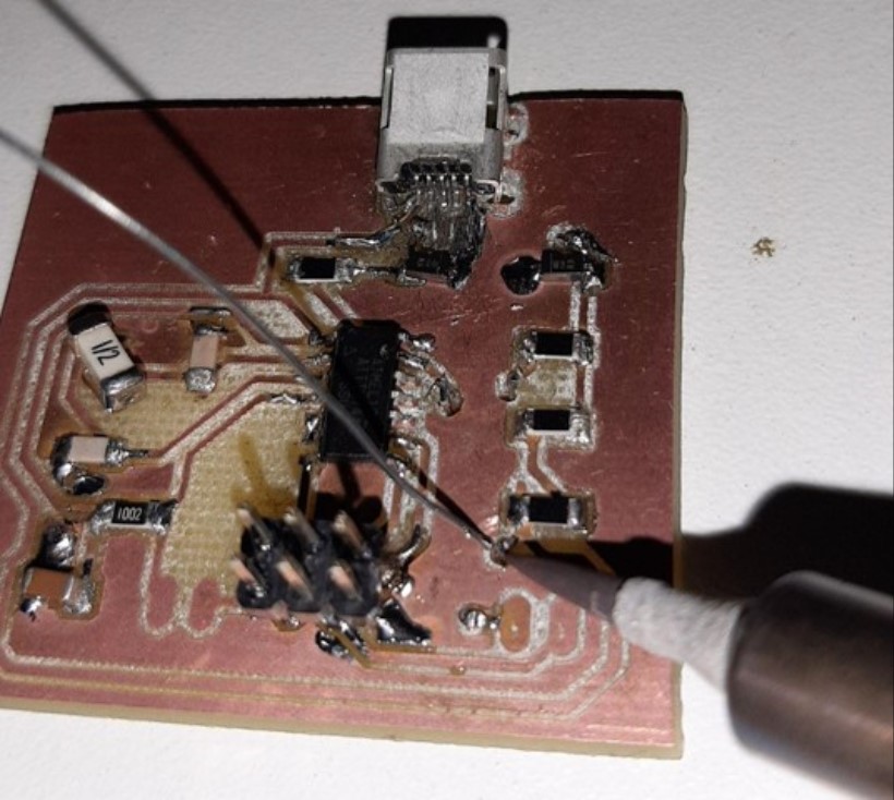
Then each component was placed in position with the help of the tweezers.
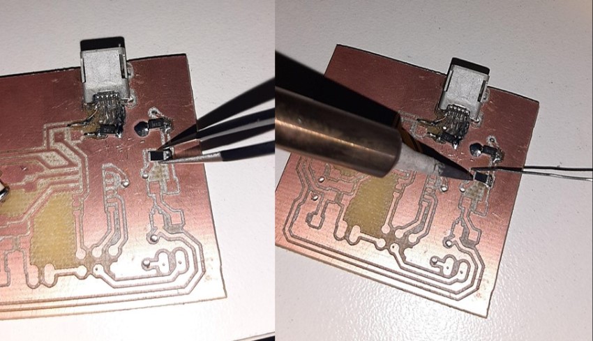 With the help of the soldering iron, the solder wire was melted at each end of the component.
After finishing adding all the components, small jumper wires were prepared for the jumpers to be added to the back of the board.
And the board was finished with the help of the soldering iron and more solder.
Test it to verify that it works
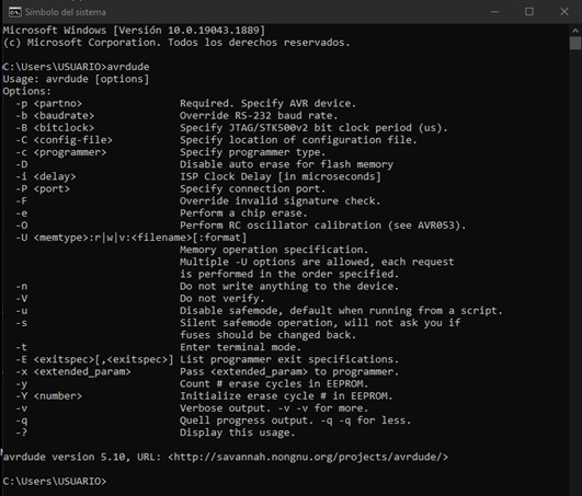
To verify that the board works we did the following test: - Downloaded WinAVR from http://winavr.sourceforge.net/download.html - Installed it by following the steps below http://www.ladyada.net/learn/avr/setup-win.html - Verify the installation by executing the avrdude command from the windows terminal.
- Install the USBTinyISP drivers from https://learn.adafruit.com/usbtinyisp/drivers
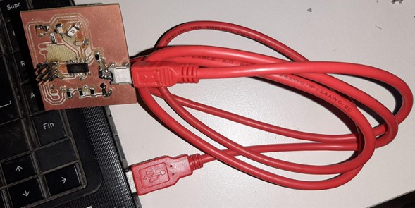
- Connect the designed board.
- Open the device manager in Windows and verify that USBtiny appears in our devices.
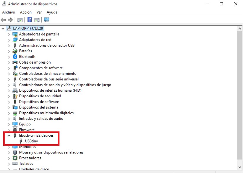
This verifies that it is working properly