7. Electronics Design
-
V = I x R
-
P = I^2 x R = I x V
Pre-work
-
SparkFun tutorials
-
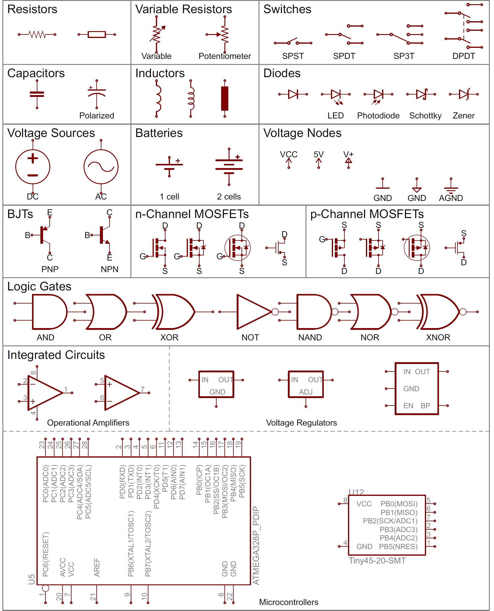
Symbols:
-
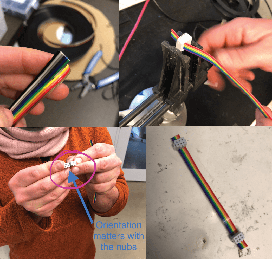
Making a ribbon jumper cable:
Eagle 101
-
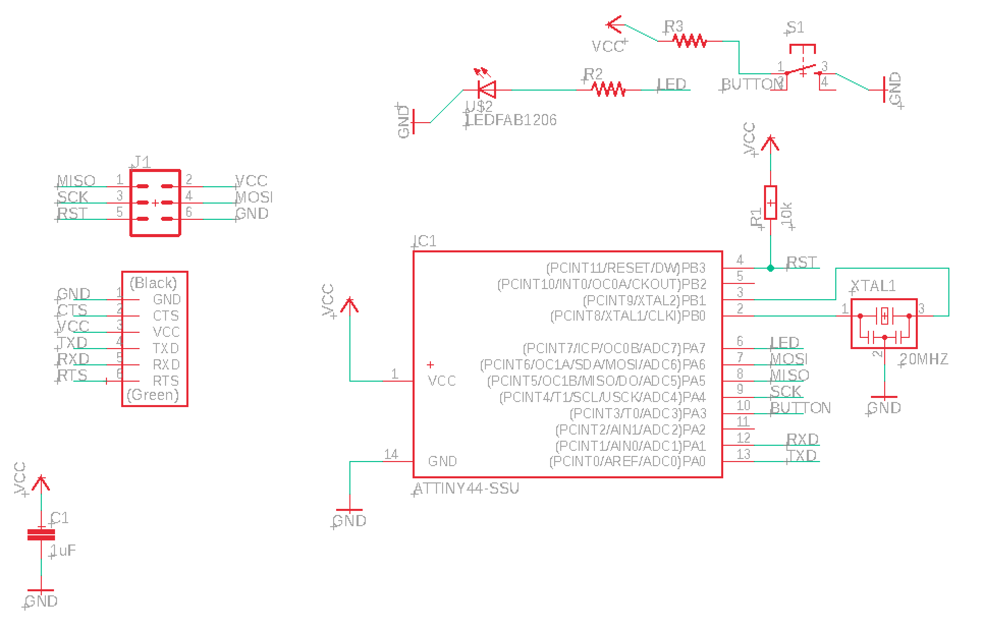
Here is my first schematic and board layout attempt at following the Fab Academy tutorial on Eagle. Un-ratsnesting the mess of lines (air wires) into traces (routed paths) was both fun and maddening, and I have low hope at this point that this board will be functional:
-
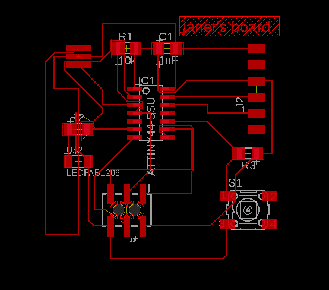
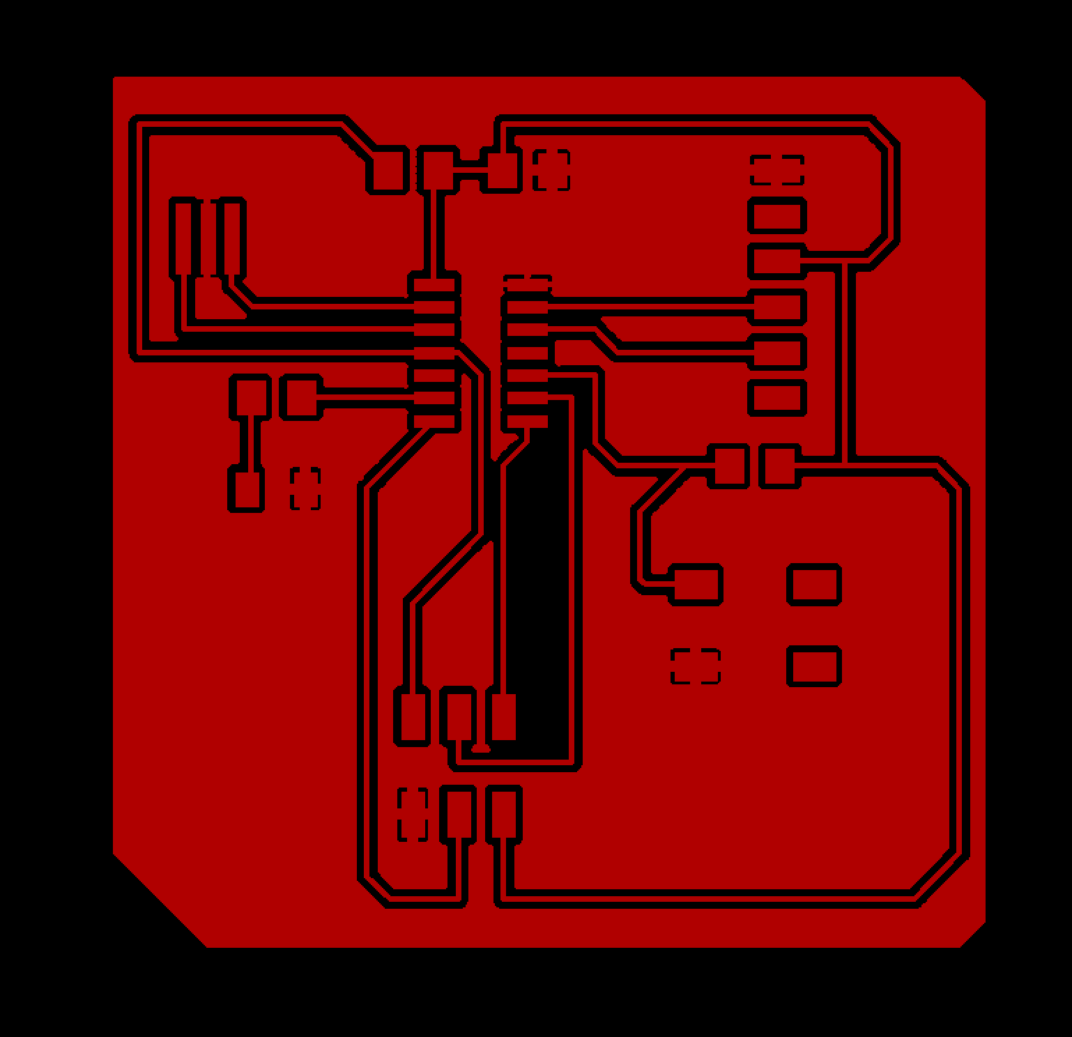
Take 2: after checking in with the Dessault crew I started over in Eagle and went with a re-design utilizing a GND copper ‘pour’ approach (see section below for thoughts and feels on the process).
-
I ran the fabmodule.dru Design Rules (DRC) linked on the Fab tutorial which analyzes clearances and such, and I was able to adjust a few minor things in my design to get the DRC to run without issue, so now we will cross fingers and pray to the pcb lords and lordesses that it actually works. (Note: only used the DRC check, not ERC-electrical rule check)
-
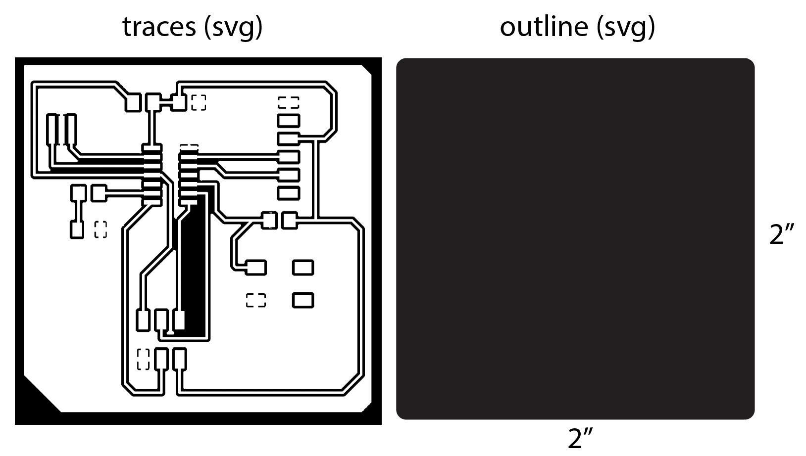
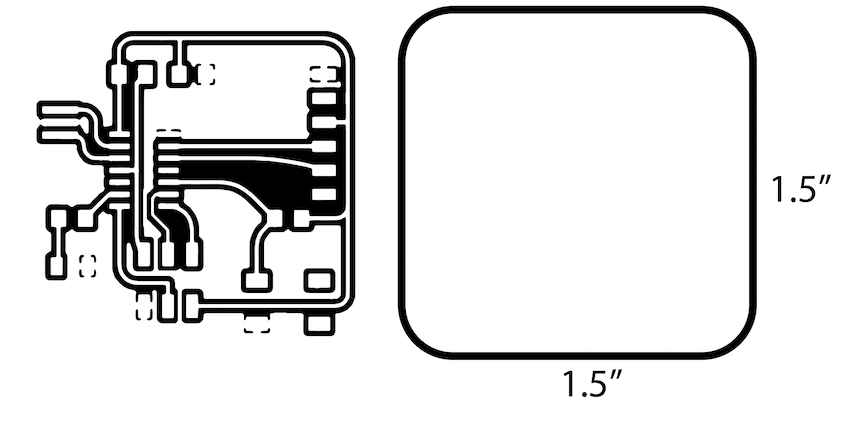
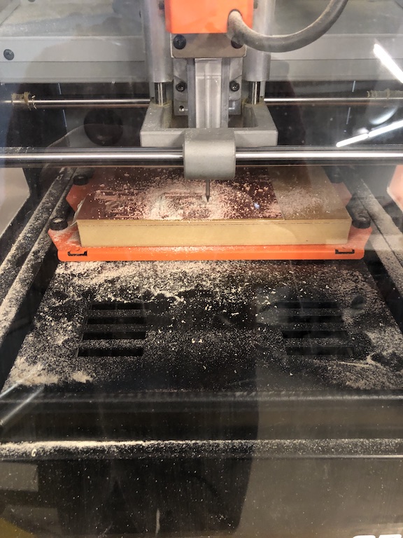
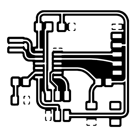
Then exported as an SVG, found that the scale was off (exported at 2x what it should have been). Compensated for this in Illustrator and resized the files and created an outline as shown below. These files are ready to test on the mill:
-
Well… we got some issues:
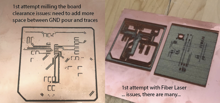
-
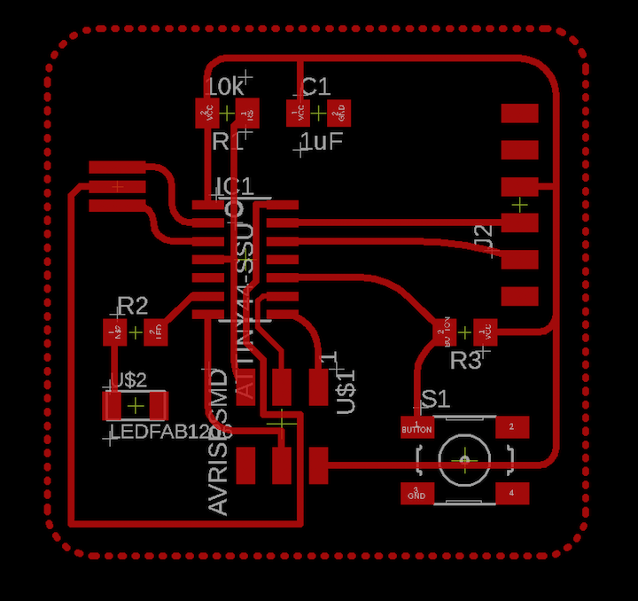
Back to Eagle to rework the board layout and trace offsets. The schematic ended up the same as the picture above– I wasn’t able to Move or Rotate components in the board view until I remade the entire project. Cliffnotes: frustrating, disheartening, sad; started from scratch, followed the board layout in the tutorial much closer, tried ground pour again with Isolate = 20 mil and Traces = 16, made a thing:
-
Used rounded traces for aesthetics; not sure if this is advisable, but it was an element that I was able to explore because it felt more organic, like drawing.
-
I did try Auto-Routing at one point but it was chaos (did not take a picture) so I went back to routing manually, which in reflection, probably had deeper learning outcomes because the second board I made (in the future from this post) went SO much smoother than this first one.
-
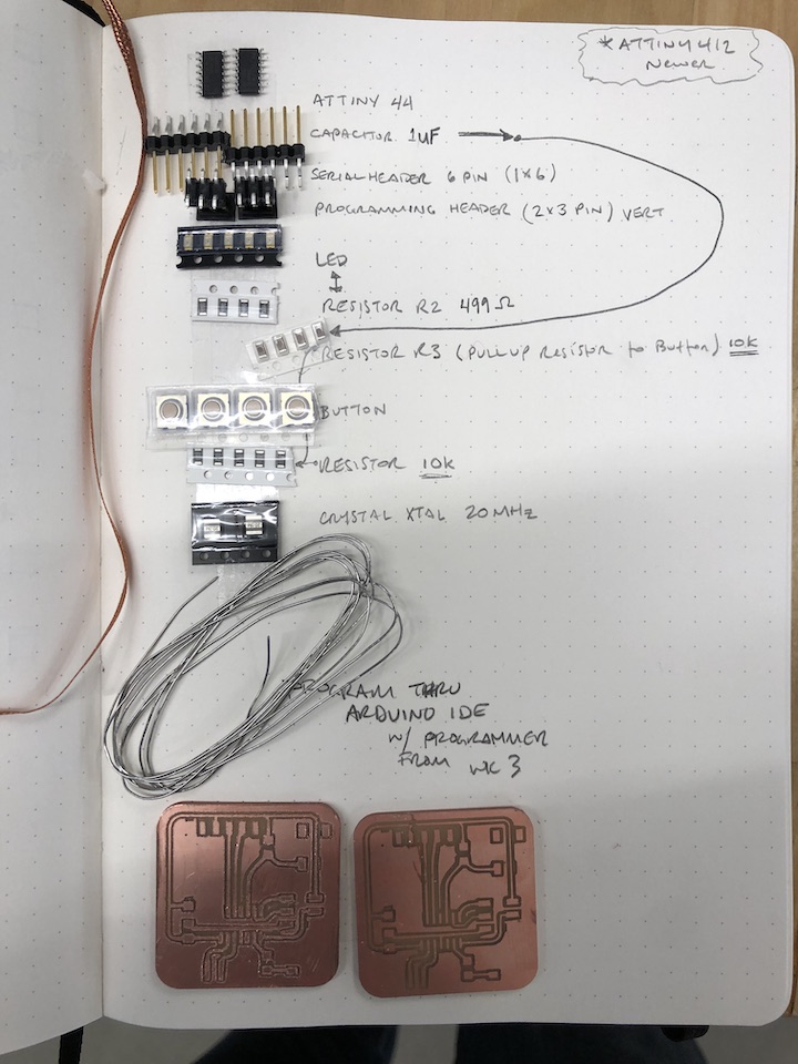
The build out! Remember: the banded side of the LED is the cathode side (negative) and goes to ground. Had some issues with the Crystal picking up the thin copper trace, this will be the first suspect if the board does not work.
Comments: choosing specific components: this was based entirely on the guide I was following linked above. I was very new to all things EE so leaned heavily on the tutorial; I will get into calculating resistor values later with more advanced boards. In general Eagle was very frustrating, many of the properties of components are not made available unless you know to click on a VERY specific location of the graphic.
- Putting it all together:
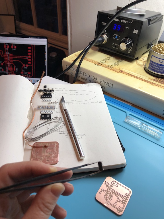
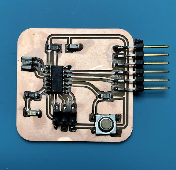
- Testing! (it worked!)
Feeling Feels:
I ran into some weird routing issues, so went with the strategy of routing VCC first and GND last- using the polygon fill option for GND. It was hard to adjust the spacing around the traces in Eagle; it is not easy or intuitive to adjust (ISOLATE is the setting to adjust this, not SPACING and you need to right click on the edge of the polygon to access those parameters, and units are mysterious and unmentioned, but I believe now, after inconclusive googling, that everything is in mils by default). If it weren’t for the awesome team at Dessault (shoutout Spencer and Nick) to assist with the troubleshooting and random mysteries of Eagle, this would have surely taken me a lifetime to figure out. #grateful #blessed
Useful links
Design Files
- Button LED Board Design Correctly Scaled in Illustrator
- Eagle Board Layout
- Eagle Schematic
- PNG Outlines *correct this file by making it a solid fill, not an outline
- Outlines RML from MODS
- PNG Traces
- Traces RML from MODS