4. Electronics Production
This week we were tasked with making and testing a Microcontroller Development board. In the new Fab Academy 2024 schedule, this is the first (of many) weeks dealing with electronics. This week’s assignment is all about the physical construction of electronics boards, meaning cutting out traces on a Copper Clad Board and attaching electronic SMD components. It doesn’t deal with the aspect of designing a board or programming a SOC (system on a chip). Those will come in later assignments.
Group Assignment
This week’s group assignment is to “Characterize the design rules for your in-house PCB production process”. And also “document the workflow for sending a PCB to a board house”.
I am a continuing Fab Academy student; me and my group all worked together on the group assignment last year, and the results are here: Electronics Production group assignment.
However 2023’s group assignment didn’t have the PCB board house component, so I documented it one the bottom of this page: Workflow for sending a PCB to a board house
Individual Assignment
“Make and test a microcontroller development board”.
Rewritten assignment
- I initially did this assignment in a previous cycle heavily documenting the production of the Quentorres RP2040 hello board design given to us.
- I had a lot of issues with the software used for generating the toolpathing for cutting my traces. I didn’t want to lose all that insight, since I thought they were a great learning experience and may be useful for other students who might encounter similar problems.
- I later made my own board that I designed in the electronics design week. Instead of removing the detailed explainations from when I initially wrote the assignment, I decided to instead just add in extra notes and pictures from my personally designed board.
Board Design
Development board
I won’t be designing the board myself. Instead I made the Fab Academy’s recommended board, the Quentorres RP2040 hello board, a development board based on the XIAO RP2040 microcontroller. I won’t be making the Quentorresaurus board just yet. The purpose of a development board is to be able to easily connect “things” to your microcontroller to try programs on it. The “naked” SEEED rp2040 board would be difficult to use without building a larger board around it since its connection points are small and very close to one another. Making a development board helps alleviate this problem.
Here are the original files given for this test board:
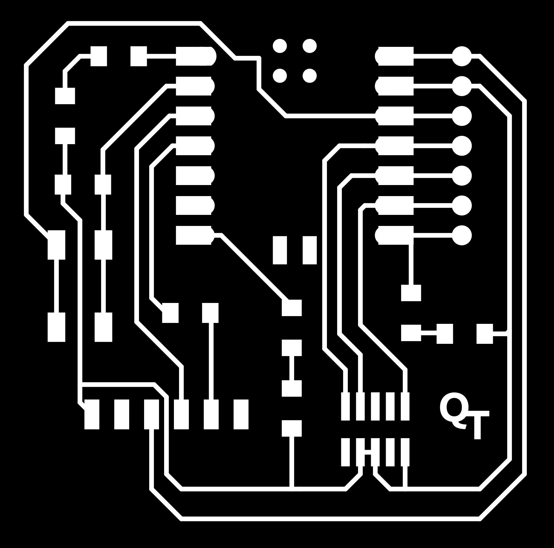 Quentorres Hello board traces
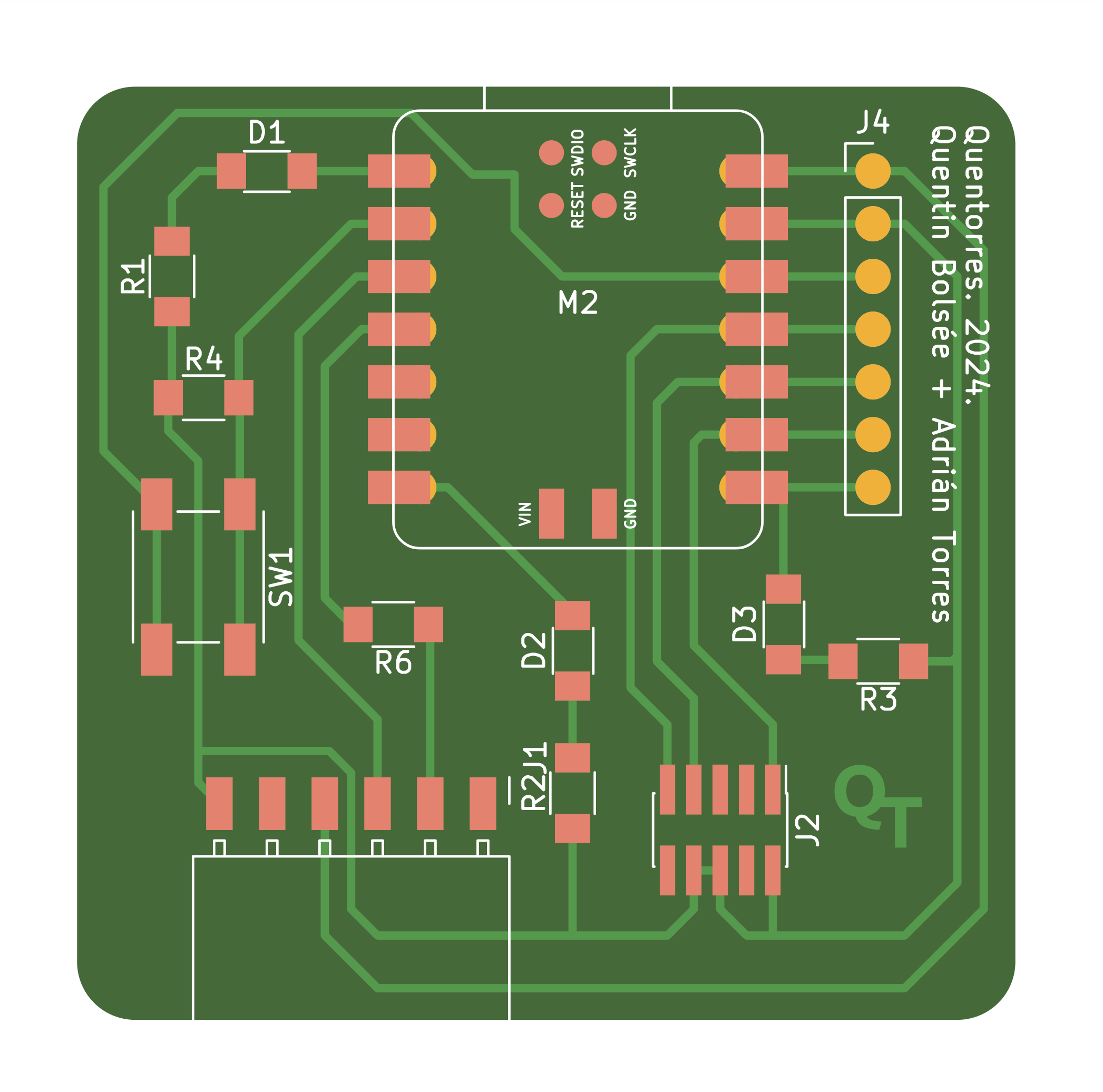 Quentorres Hello baord Gerber Layout
 Quentorres Hello baord drill holes
 Quentorres Hello interior- board cuttout border
My Design (Update)
My Board Design was developed in electronics design week, so you can see the details there. The final design file that I needed for producing my board was the SVG file.
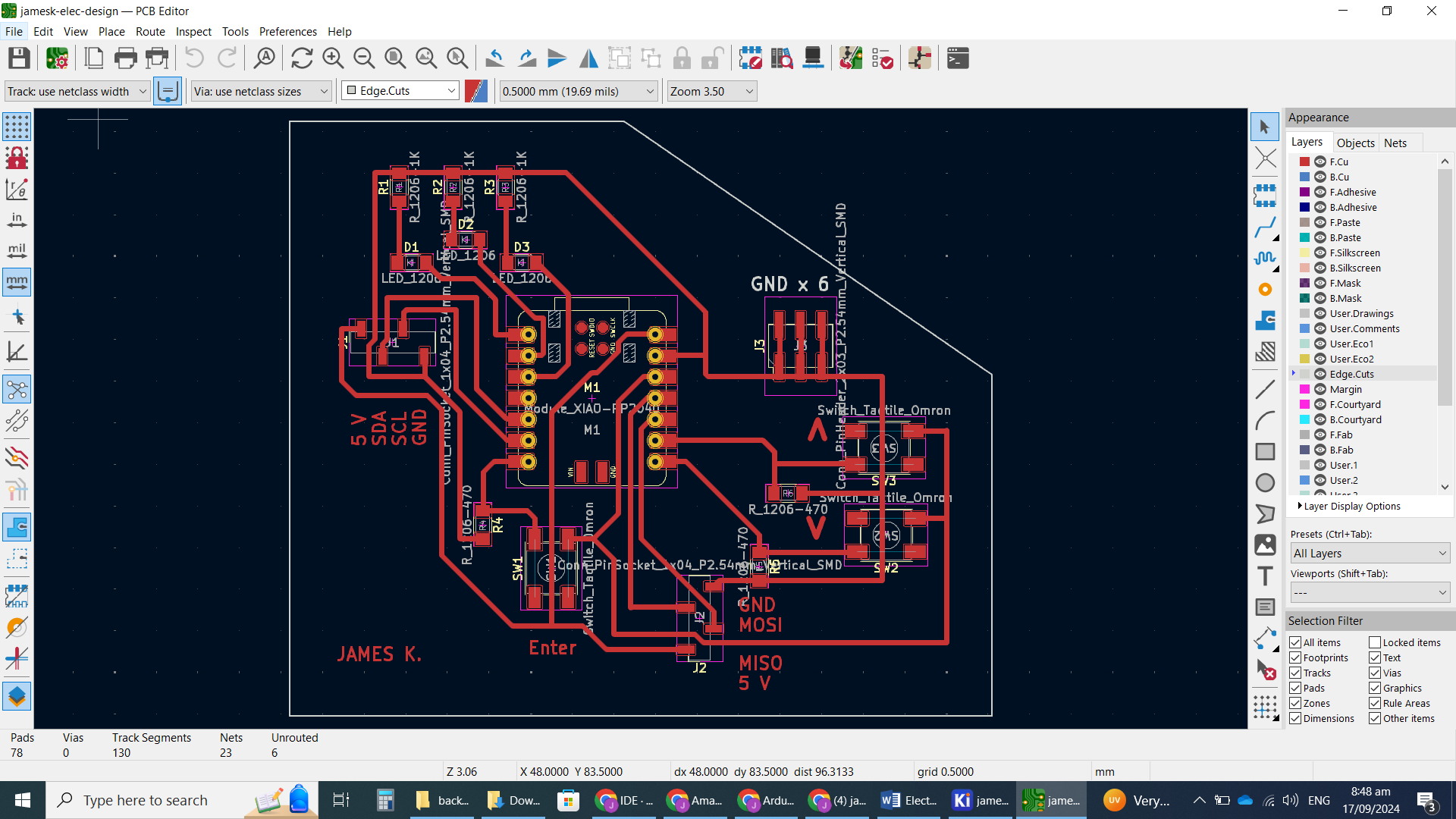
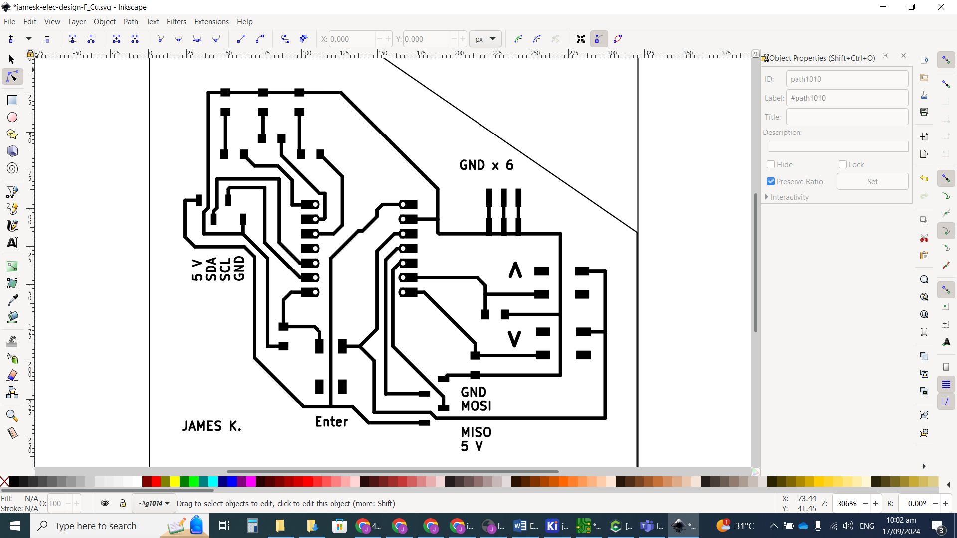
generating toolpath
Development board
I had a lot of problems developing the toolpath for milling the board. It should have been a fairly straightforward process since we were given the design. I will try to articulate my issues here: problems with toolpath.
I used Carbide Create to generate my toolpath. Our precision desktop CNC mill is the Carbide3D Nomad 3. Carbide 3D are also the makers of Carbide Create, so it was the recommended software for generating the toolpath.
I began by dragging the main traces file into the workspace. I then clicked on the “Trace image” button to extract the traces from the image.

The 2nd thing was to set up the job by clicking on “Job Setup” under “setup” in the top left panel. I measured the dimensions of my blank FR4 copper clad, using a ruler for width and height, and a Vernier caliper for thickness. I probably should have done this as the first step before importing the traces.

I then selected all the traces and clicked on resize to get them to the intended size. NOTE: I didn’t particularly like the fact that importing the PNG seemed not to keep dimensions, so there could be a potential for problems if resized incorrectly.

- I wanted to make my board with only the desired traces left behind, that means cutting away all the unwanted copper instead of just tracing the boarders of traces. I wanted to do this because I am not very good at soldering, and doing this type of “pocket” milling means that there’s less chance of me accidentally creating shorts with poorly done solder connections.
I clicked on the “Toolpaths” tab, and clicked on “pocket”. I then selected the desired bit. I wanted to cut my board using endmill bits rather than a V-bit. From my research, endmill bits tend to give better results than V-bits. This is because using endmills meant we didn’t have to worry about cut depth the way we would with a V-bit. We also didn’t have to worry as much about any slight unevenness in the copper board.
The Carbide create software has a number of preset bits that are sold by them as well. Out of all the main endmill bits that we bought with our Nomad 3, the # 122 carbide 3D endmill has the smallest tip diameter (1/32 “), so I chose this.

When I completed the modeling of the pocket cut, I got this:

I highlighted a couple problems.
-
The biggest issue was that for some reason the toolpath seems to be completely cutting away some of my traces (red circles); I discussed how I dealt with this in the problems with toolpath below.
-
The other issue was that some of the details of the traces were not being cut (green circles). This was to be expected because the #122 endmill cutting diameter wasn’t small enough for the thinned cuts. I solved this by adding a contour cut on all the traces with missing detail using a finer bit.
After “fixing” the toolpath problems for the deleted traces, I was got here:
 My solution for the deleted traces was a bit inelegant, but it got the job done. (I didn’t bother fixing the removed J J in my initials in the corner since it wasn’t needed)
To do the contour toolpath I had to use a smaller tip endmill. We have a 1/64” carbide depot endmill on hand.
I needed to add this to the bit list in carbide create.
Under the “select tool” menu, I scrolled down to the bottom and selected “add tool”.

from there I looked up the recommended settings for the bit and entered those values.

I then selected all the traces with the missing detail in order to do a contour cut around them.


The final step was to select the outer border line of the circuit and set it up as another contour toolpath, this time again with the #122 endmill. But this was set to cut the entire depth of the copper board so that it could cut it out.
I then saved the completed toolpath file to load into the software to do the milling.
My board (Update)
-
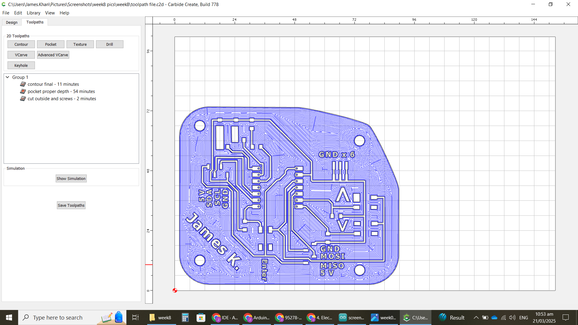
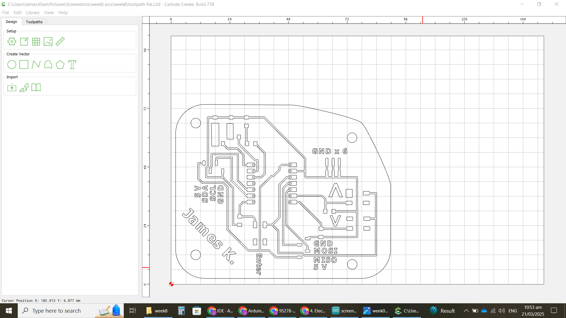
I did the same procedure for generating my personal board’s toolpath as I did for the development board above. And the end results were the same.
-
I made some minor changes to the board in the Carbide Create software itself. Most of them were not related to the circuit’s traces, instead they were things like labels on the board and cutouts for screw holes.
-
I did make some changes to the actual circuit traces and these are discussed in the [Problems with pocket toolpath] section.
-
My board took longer to cut than the development board (as expected), because it was a bigger board with more details.
-
I encountered the same types of problems generating the toolpaths for my personally designed board as I did for the development board, and had to make some similar alterations.
Heres the Carbide Create File for my board.
Problems with pocket toolpath
Development Board
I had allot of problems with the pocket toolpath cutting away 2 sections traces and pads that it shouldn’t. (highlighted in red)

I spent hours trying to fix the problem. I tried - editing the original png. - shifting the location of the traces on the material. - smoothing out the traces curves. - redrawing the traces. - redrawing and altering the outer boarder. - and a bunch of other things and combinations of the above steps.
However the problem kept repeating. I was going to give up and resolve to just use contour toolpaths only, but I really wanted to know what I was doing wrong so I could become better with the software.
Eventually I decided to update the carbide create software itself. When I found the update web page I found the changes list for each of the release builds. There were a number of fixes relating to pocket problems. I updated my software but still got my problem. I am pretty sure that the problem resides in a bug in the pocket toolpath code rather than an error I made.
In playing around with fixes, I did realize that if I made the “missing” traces big enough, they eventually were being detected properly. It was faster to do these changes within the carbide create software itself, rather than going back and forth with design files or image editors.
Of course I couldn’t just make the traces or pads arbitrarily big and still fit the components properly. Eventually I settled on expanding the deleted traces into large rectangles that would act both as big pads where 2 components can both be soldered onto. You can see below how the two drawings differ, with the original on the left.


Hopefully they can fix this error in the software in the future.
My board (Update)
-
I encountered the same types of problems generating the toolpaths for my personally designed board as I did for the Development board.
-
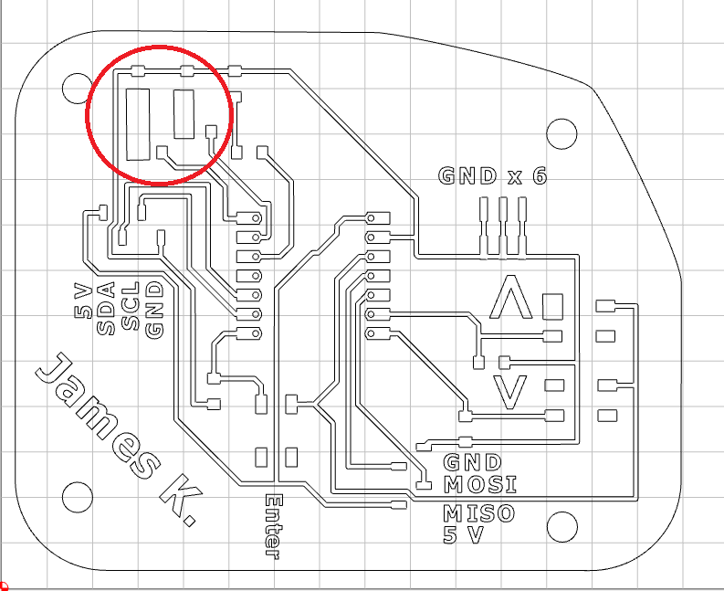
The solutions also ended up being the same. Small alterations to some pads and traces that were being erased.
-
Seeing what ended up working was a bit of trial and error, just like before. The area circled in red below is the area where I was forced to make design alterations to account for the toolpathing errors in Carbide Create.
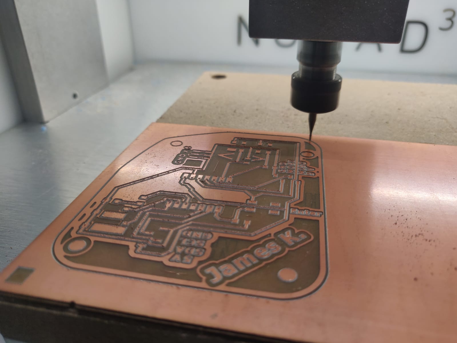
milling the board
Development Board
Milling the board was relatively simple.
Setting up the material:
-
I put a few strips of double sided tape onto the bottom of my bland copper clad board.

-
I then stuck it down to the wasteboard of the NOMAD 3.

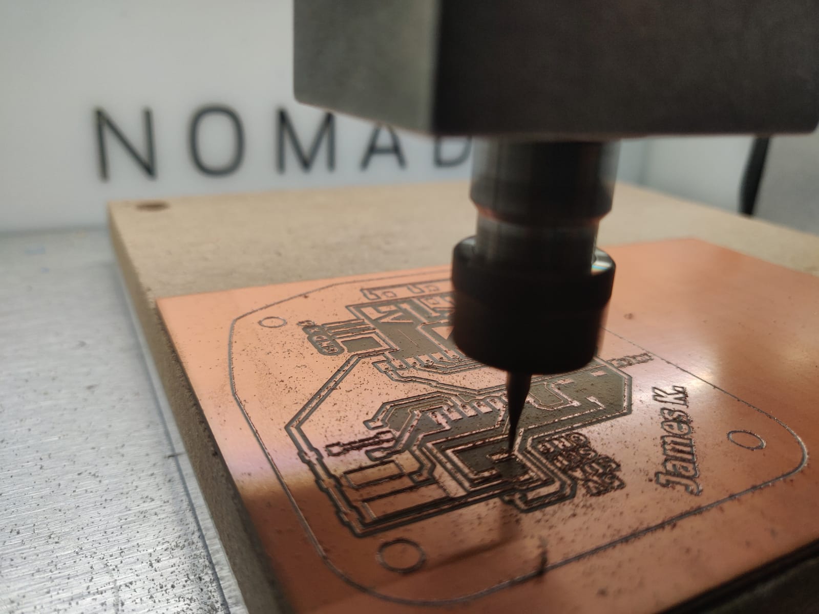
I used carbide motion software to control the CNC mill.
Steps:
-
Connect the Nomad 3 to the computer by USB and turn it on.
-
Click connect to cutter in the software.
-
Install the endmill bit into the collet.

-
Connect the zero probe to the machine.
-
Select jog from the top right in the software, then use the buttons to manually bring the bit into the circle of the zero probe. Then click probe.

-
Load the toolpath file we saved in carbide create.
-
Select “run”.
-
The software asks you to verify that correct bit is installed and then begins cutting. It began with inside contour cuts using the 1/64” endmill.
-
Once this was complete, it stopped the spindle and asked for the bit to be changed to the #122 1/32” endmill. I then clicked continue.
-
It performed the pocket cut, and then cut out the board’s outer perimeter.
youtube video:
same video local copy (lower quality):
Finished cut board (before removing)

The completed board was then pried off the wasteboard. Then it was washed with a mild soap and lightly scrubbed with a mildly abrasive pad to remove lose material from the milling process.
My Board (Update)
The procedure for milling my board was the same as the developmet board. It was just a bigger finished product and took a little longer to mill.
adding components to board
Development Board
For a couple of the components we didn’t have all the exact models indicated in the instructions, however we had alternatives:
-
LEDs. I swapped out the 3 LED BLUE CLEAR 1206 SMD for LED BLUE CLEAR CHIP SMD BOT ENT
-
6pos connection header. We didn’t have the CONN HEADER SMD R/A 6POS 2.54MM so instead I used CONN RCPT 8POS 0.1 GOLD SMD R/A. I simply left the first 2 contacts on the 8pos unsoldered.
First I put the board under a microscope with a screen to more closely examine it.

The board looked pretty good except for one error I missed in the toolpath. There was a pad still joining a trace that was not separated. This was because I didn’t realize that the pocket toolpath had missed it, so I didn’t include that trace in the contour toolpath.

I simply fixed it by using a hobby knife to removing the joining copper.

I placed a piece of tape on the back of the main board for the chip. This was to prevent the contacts on the back of the chip from accidentally shorting out on a trace on our board. This wasn’t really necessary, since I used a pocket mill, but I still did it.

Then I soldered all the component onto the board:
-
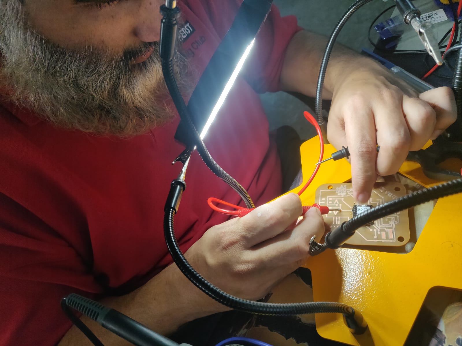
I used a magnified third hands with build in light to help hold the components together and magnify what I was working with.
-
I used a Hakko soldering station and lead free solder.

-
I am not great at soldering, but I was able to get it done.
-
I then used a multimeter on the continuity setting to test traces and pads that were next to each other on the board to ensure that I didn’t accidentally bridge anything that wasn’t supposed to be while soldering. Luckily I didn’t make any errors soldering.
You can see the finished board in action in the youtube video below while testing the board.
My Board (Update)
-
The procedure for soldering components to my circuit board were the same as for the development board.
-
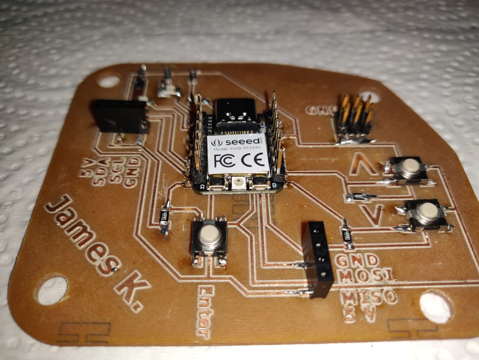
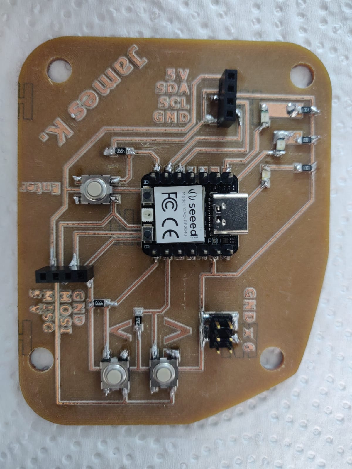
The components I had to mount onto my board were:
- 1 microcontroller SEEED rp2040
- 3 LEDs LED RED CLEAR 1206 SMD
- 3 Buttons B3SN-3112P
- 3 Resistors 1 KiloOhm (RES SMD 1K OHM 1% 1/4W 1206)
- 3 Resistors 470 Ohm (RES 470 OHM 1% 1/4W 1206)
- 2 female 4-pin connectors female CONN HDR 4POS 0.1 TIN SMD
- 1 male 6-pin connector male CONN HEADER SMD 6POS 2.54MM
Testing the board.
- I connected my development board to my laptop using a USB-C to USB-A cable. The red Power LED and User green LED near the USB connector lit up so I knew I was getting power.
- I followed the instructions on the Quentores Xiao RP2040 project page to set up the Arduino IDE software and select the proper board.
-
To test that my development board was working properly, I wanted to run the “Blink” test program. This can be found in the software under “Files - Examples - 01.Basics - Blink”

-
The blink program didn’t work right away because the PIN that the output signal was being sent to didn’t coincide with the output pins that the external LEDs were connected to on my board. My LEDs with wired to pins D0, D6 and D7, which correspond to port 26, 0 and 1 in the ARDUINO GPIO.

-
I altered the program so that it turned on all 3 LEDs in sequence then turned them all off in sequence.

Here is the program code (minus the introduction comments):
// the setup function runs once when you press reset or power the board
void setup() {
  // initialize digital pins 26, 0, and 1 as an output.
  pinMode(26, OUTPUT);
  pinMode(0, OUTPUT);
  pinMode(1, OUTPUT);
}

// the loop function runs over and over again forever
void loop() {
  digitalWrite(26, HIGH);  // turn the LED 1 on (HIGH is the voltage level)
  delay(500);                      // wait for half second
  digitalWrite(0, HIGH);  // turn the LED 2 on (HIGH is the voltage level)
  delay(500);                      // wait for half a second
  digitalWrite(1, HIGH);  // turn the LED 3 on (HIGH is the voltage level)
  delay(500);                      // wait for half second

  digitalWrite(26, LOW);   // turn the LED 1 off by making the voltage LOW
  delay(500);                      // wait for a half second
  digitalWrite(0, LOW);   // turn the LED 2 off by making the voltage LOW
  delay(500);                      // wait for a half second
  digitalWrite(1, LOW);   // turn the LED 3 off by making the voltage LOW
  delay(500);                      // wait for a half second
}
my edited blink program (download)
Here is a video of the blink program running on my board: BLink program working (youtube)
Lessons learned and future plans
- The default trace lines given in most design programs are often thinner than needed, and sometimes closer than needed. This can lead to:
- broken traces when milling, because the traces are so delicate and/or your fine endmill is a little dull.
- Areas not being milled. This because they are so close that the endmill can’t cut the space between two traces without cutting the traces themselves, so they just don’t cut at all.
-
When using the design software in future weeks’ assignments, I intend to increase the trace sizes wherever viable, and increase the gap between traces if I can. If this can’t be done automatically in settings, I will have to do manual edits.
-
Although I didn’t design the board used this week, I should have edited the trace schematic when I saw certain issues pop up:
- 1 gap didn’t get cut. This was the gap between the pad for PIN 1 of the Xiao 2040 board (top left) and the diagonal trace above it. In making the board I left this uncut by the machine, and instead cut it manually with a hobby knife afterwards. In retrospect, it would have been easy to move the diagonal trace to the right and give more space so that the endmill could have cut it.
- There was a bigger issue with the milling software deciding to mill over 2 sections that were not supposed to be cleared out. I spent a day and a half trying to figure out why, but to no avail. We run our Fab Lab here, so if we intend to teach this topic I wanted to be able to solve this problem rather than use a workaround (which is what I had to end up doing). I ultimately couldn’t find out what went wrong without spending even more time on it, and I had to resign to using a workaround by drastically changing the shape of the problem traces, while still being functionally the same. I still never figured out why Carbide Create pocket toolpath wasn’t detecting a few zones of the design properly, because contour and texture toolpaths detected them fine.
-
Use bigger pads and contour toolpath instead of pocket toolpath. Initially I chose pocket toolpath because I don’t have much faith in my fine soldering skills. Pocket toolpaths are more forgiving for poor soldering, because if you spill over, you are likely spilling into empty non-conductive space; with contour toolpath, if you spill over you are likely making contact with conducting copper and creating a short circuit. The problem with pocket toolpaths is that they take allot longer to cut (plus I was having pocket toolpath issues in Carbide Create as indicated above), wearing down the expensive precision endmills (1/64 inch tip and smaller). The compromise here is use contour toolpaths with larger solder sites, so the board is still more forgiving for mediocre soldering skills, while not overusing the expensive endmills.
-
Use a “roughing” toolpath. For my board, I used a 1/32 endmill for a pocket toolpath, then a 1/64 bit for a contour toolpath. This worked well, however there were long sections of certain traces that the 1/32 bit did well, but doing the 1/64 contour was superfluous. My plan for the future though is to refine this method. I don’t need to do pocket toolpaths if my main endmill is 1/32, since this gives me enough clearance for my mediocre soldering. Once the software plots the 1/32 toolpath, it SHOULD be easy to edit the vector sections for the trace layout to be able to specify only the areas that the 1/32 pass missed (or that are good enough). Then I just need to contour those sections alone with the 1/64 bit to get my final layout. I just need to be careful not to cut across existing trace lines when doing my finishing pass.
-
Hopefully use a solder paste stencil in the future. As I keep saying, I am worried about my solder skills. I know that solder paste stencils are a great solution. After a fair amount of trying, me and the rest of the students here at our lab have not had success getting solder paste to work (there is a chance that the problem is with the paste we have on hand itself). I hope to be able to solve this and use a solder paste stencil for my future projects.
Sending to a Board House
In the real world, you are very unlikely to mass produce your designed circuit boards in a Fab Lab, or even if you are a small company, in-house. Fab Labs are great for prototyping and design, but when it comes to mass production not so much. For many product types you need to create a specialized manufacturing system or assembly line in order to produce your item at scale and with consistent quality. For circuit boards the cost of creating an assembly line are so high that in order to mass produce the only financially viable option is to outsource the board production to PCB board houses.
The process of sending to a Board House is as follows:
-
Design your board 232pm test
-
The first step in mass production of a circuit board it to design the board itself. You need to pick the components you would need and design your trace layout in software like KiCAD or Fusion360. Usually your first working design is more powerful and complicated than it needs to be. eg:
-
You pick a SoC that is way more powerful than you need and has more input/output ports than you need.
-
You have connectors for programming that are only needed once, or ports you don’t need.
-
You have extra ports and connections dedicated to troubleshooting.
-
Your design is likely too big for the space required for the project as a whole.
-
-
Finalize your board
-
Once you have your first working design, you need to “trim the fat”. All those extra components, connectors and traces from your initially design that aren’t strictly needed for your production model should be removed.
-
Finalizing your board is an iterative process, where you would produce multiple versions, each trying to hone in on the cheapest reliable design that still works as intended. Common things to change:
-
Downgrading your chips. For troubleshooting convenience we often design our circuits using components that are way more powerful than needed. Downgrading these chips to the lowest power that doesn’t affect final performance means much cheaper production costs.
-
Removing unnecessary ports and connectors. This includes the connectors we used to program the onboard chips during design. In your final product you won’t need to reprogram your chips, so it’s easier to program them before soldering them to the board. Fewer ports (both chip pins and as external connectors) means saving money.
-
changing the shape of your board to fit the cavity or space it will be occupying in our final product.
-
-
IP Protection. If your board design is novel enough and you think that people stealing your design can significantly hurt your business, you may want to file for a patent, however this is an expensive and lengthy process. Getting copyright protection for your design is much simpler and cheaper but offers allot less protection against “bootleggers”.
-
-
Find a Board House
-
The next step is to find a board house that you can hire. There are quite a few reputable ones out there like:
-
Which one to pick is personal choice for your business. You may have factors that limit your choice such as:
-
Not wanting your boards made in certain countries. Perhaps for moral or legislative/tariff reasons.
-
The reputation of the supplier for reliability and quality.
-
The turnaround to get your product.
-
The capabilities of the company especially if you have a particularly complex board.
-
-
Usually once you find a PCB house that can meet all your needs, the deciding factor is usually the price that they can produce and ship your circuit board for. But again, there can be allot of factors in picking the right PCB house for you.
-
-
Send your Design to your chosen board house
-
Once you have selected your Board House, you need to send them your design files for them to analyze and certify that they can make it.
-
Most Board Houses can accept multiple design file types, but all should accept Gerber Files.
-
There are design choices that you must stipulate that won’t be included in your Gerber files like: board thickness, strength, colour, and substrate material.
-
-
Finalize your order
-
Once the Board House verifies your design and selected options its time to finalize the order.
-
The board house will likely give you a quotation with different options. The cost per unit made will be lower the bigger your order is, so bigger orders work out cheaper than multiple small batches.
-
You will likely get options for priority with rushed orders costing more. As well as different options for shipping.
-
After selecting these final details for your order, there will likely be fine print on the contract that you may want to look over. These are things like quality control, how delays are dealt with, responsibility for customs and duties etc.
-
Once you are happy with all the details, you can agree to the sales terms and arrange payment to the Board House.
-