-
01. Principles and practices
-
02. Project management
-
03. Computer-Aided design
-
04. Computer controlled cutting
-
05. Electronics production
-
06. 3D Scanning and printing
-
07. Electronics design
-
Assignment
-
How to use KiCad
-
Individual Assignment
1. Make an ATtiny1614 board
- Issue 1. Missing symbol
- Issue 2. Wrong milling settings
- Issue 3. Bad PCB design
- Issue 4. Traces too close
2. Program the board
3. Communicate with the board
- Issue 5. No echo coming back
- Issue 6. Weird behavior
4. Control an LED
- Issue 7. Wrong pin number
5. Make a UPDI
6. Summary
-
Group assignment
-
Attachments
-
-
08. Computer controlled machining
-
09. Embedded programming
-
10. Input devices
-
11. Applications and implications
-
12. Output devices
-
13. Interface and application programming
-
14. Invention, intellectual property and income
-
15. Networking and communications
-
16. Molding and casting
-
17. Wildcard week
-
18. Machine design
-
19. Project development
-
Glossary
Week 7. Electronics design
March 10, 2020
Assignment
Group assignment
- Use the test equipment in your lab to observe the operation of a microcontroller circuit board
Individual assignment
- Redraw an echo hello-world board
- Add (at least) a button and LED (with current-limiting resistor)
- Check the design rules, make it, and test it
- Extra credit: simulate its operation
How to use KiCad
Last Thursday, Henk gave us a brief lecture about how to use KiCad. The tool was pretty straightforward to use in general, but there were some parts that made me frustrated. Let's see the general workflow first.
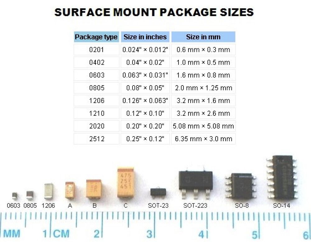
The size we used for the board was 1206
Workflow
First, download KiCad from this link
Once the download is done, open KiCad
Before starting, you can add symbol and footprint libraries. I downloaded Fab Academy ones, and added a fab.lib file to the symbol library and a fab.mod file to the footprint library (download link)
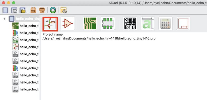
Create a new project from File > New > Project and name your new project
Click the Schematic Layout Editor button
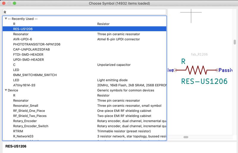
Click the Place symbol button to add a new component to your sketch. You can search components you need and select them from the library to want to use
After selecting a component, you can add it to the sketch by clicking the location you want to place it in
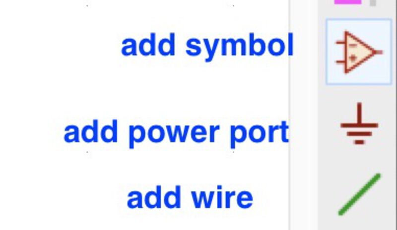
Add wires and power ports as you need
Now that the drawing is done, it's time to annotate the components. Click the button right next to the red bug button and when the popup comes up, click Annotate. This will add a number to each component
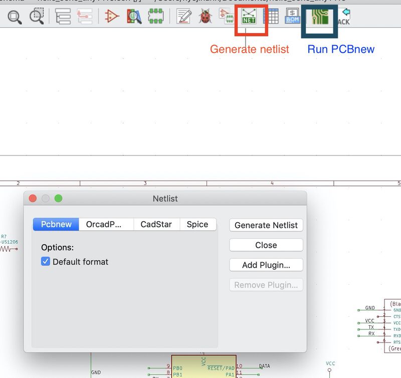
Click the Generate Netlist icon and then click the Generate Netlist button in the popup window to save it.
Once the netlist is created, click the Run PCBnew button and it will open a PCBnew window
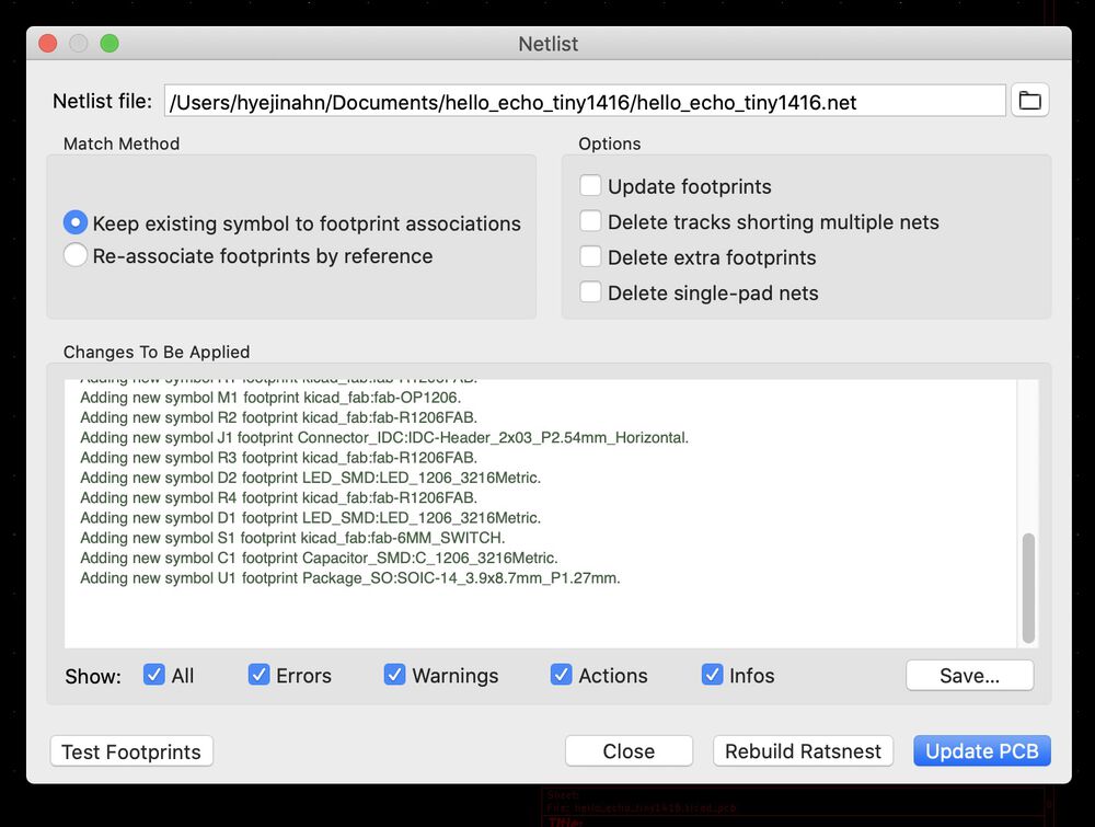
In the PCBnew window, click Tools > Load Netlist and load the netlist file you just created. And click Update PCB. If you want to update your schema, you can go back to the Schematic Layout Editor and make a change. After updating the schema, you can come back to the PCBnew window and click Tools > Update PCB from Schematic and click Update PCB
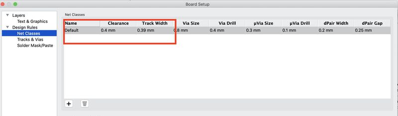
I always forget this step, but it's important. Go to File > Board setup > Design Rules > Net classes. I only changed the clearance value to 0.4mm and the track width value to 0.39mm
Then, you will see something like the photo below. From here, you need to move components around to place them in the right location. You have to think about the best location for each component so that later you can connect them all without overlapping paths
After relocating the components, draw tracks. I struggled a little while drawing tracks, because the last one or two tracks always couldn't get connected no matter what I tried. I think it was because I didn't place the components well in the previous step
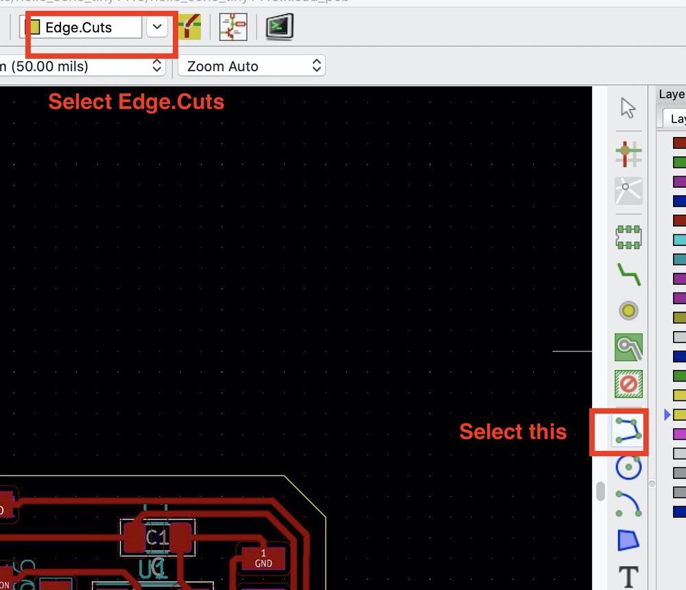
After all connections are linked, draw an outline. Select the drawing tool from the right side, and change the draw line to Edge.Cuts
And click the point where you want to start the outline and draw it one line at a time
Once it's done, go to File > Export > SVG and export the trace and the outline files. You can set the directory where the files are saved by changing the Output Directory
All done! Go to a milling machine and mill the files

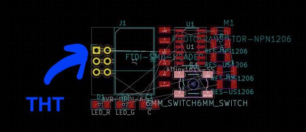
I was supposed to use an SMD component but I used an THT component accidentally in this design.
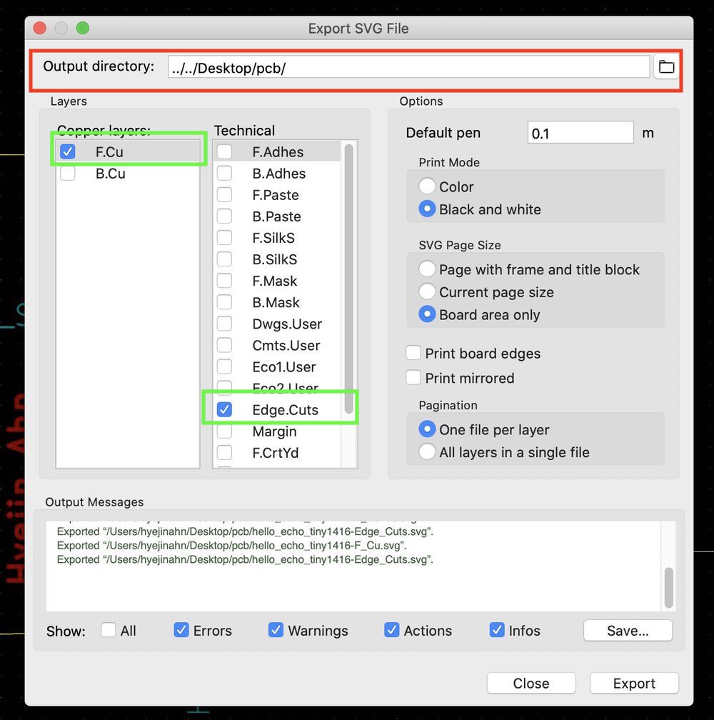
For exporting trace and outline
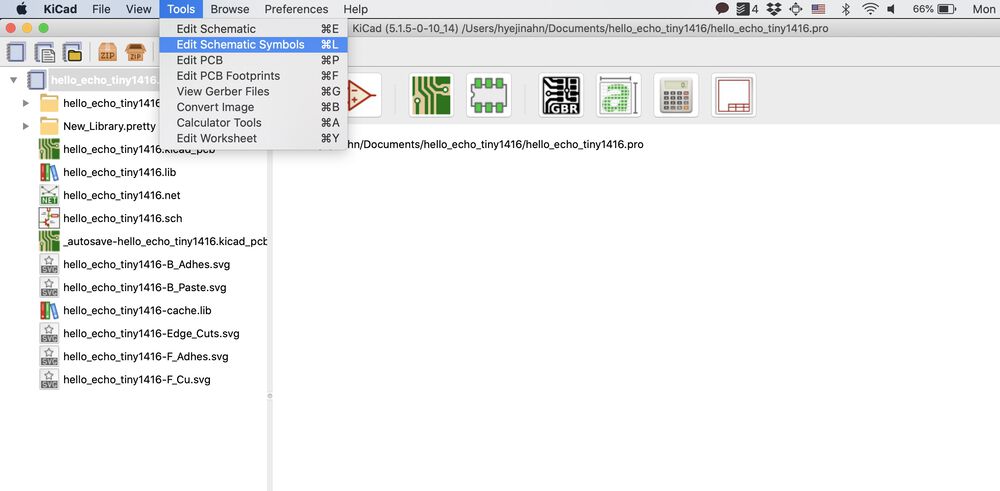
How to create a schematic symbol
First, create a project if you don't have one open (File > New > Project)
Go to Tools > Edit Schematic Symbols. This will open a Symbol Editor window
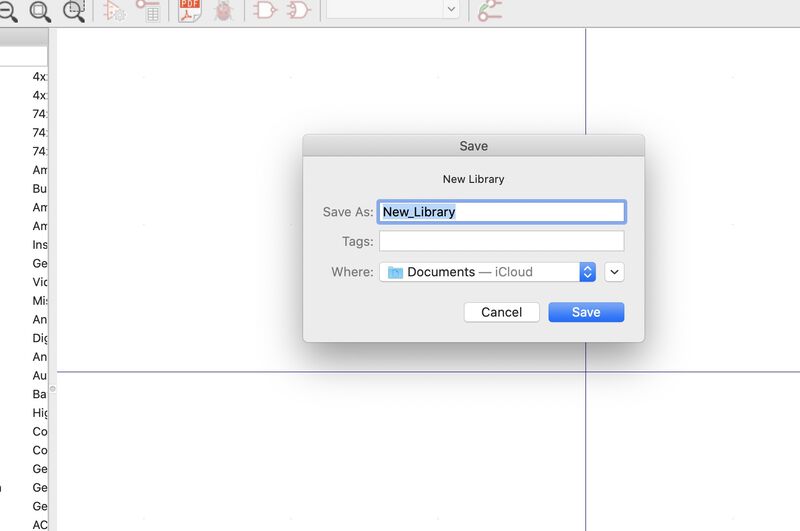
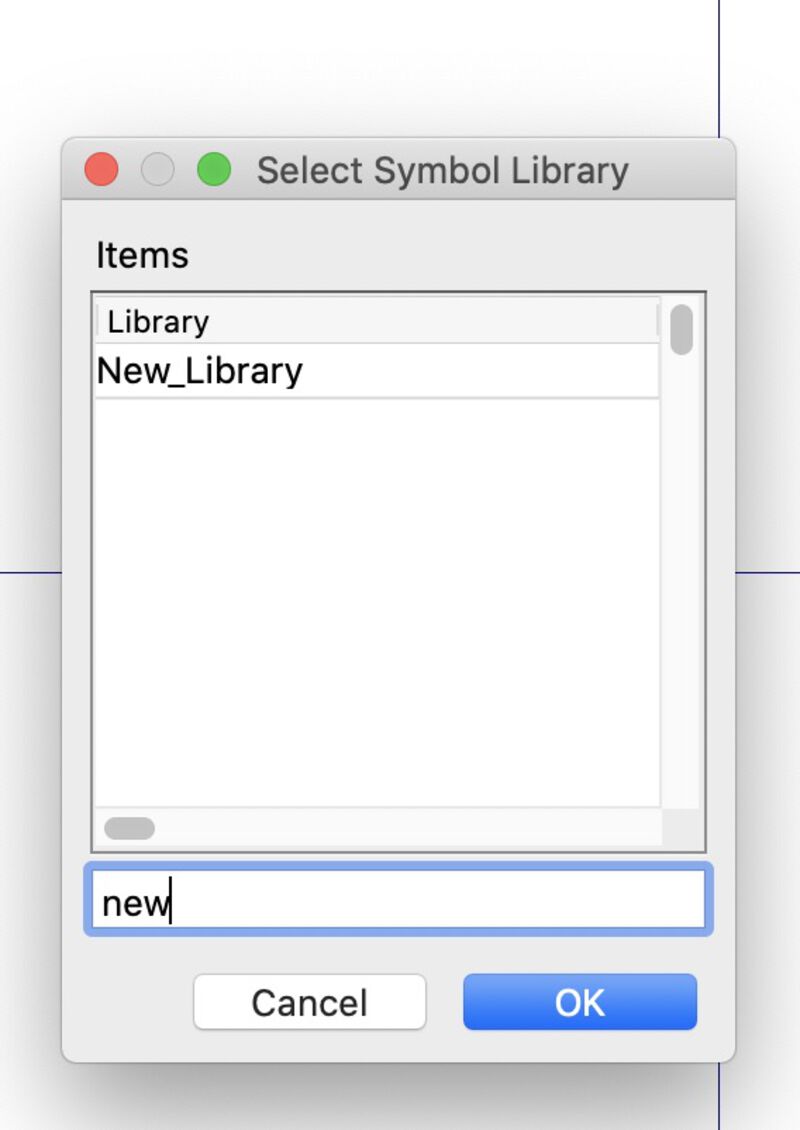
Go to File > New Library and name your library and save it. Don't add a new symbol to the existing library that you download from GitHub, because it might cause a problem syncing with the original library later
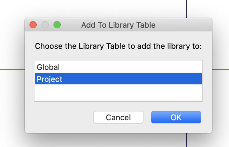
Then, select either Global or Project. I selected Project because I wanted to add this to only the project I was working on
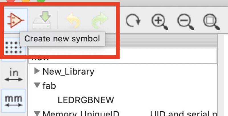
Click the create new symbol button on the top left. Search for the name of the library you just created and select it
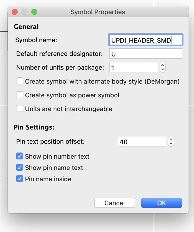
Give a name to the component (I left the other fields as is)
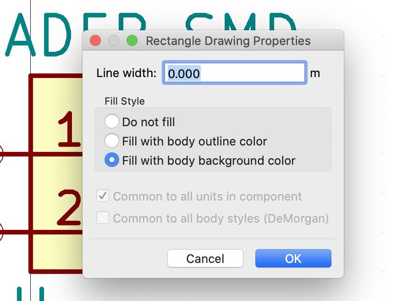
Draw a component. You can also add a background color to a component by clicking Edit Rectangle Options
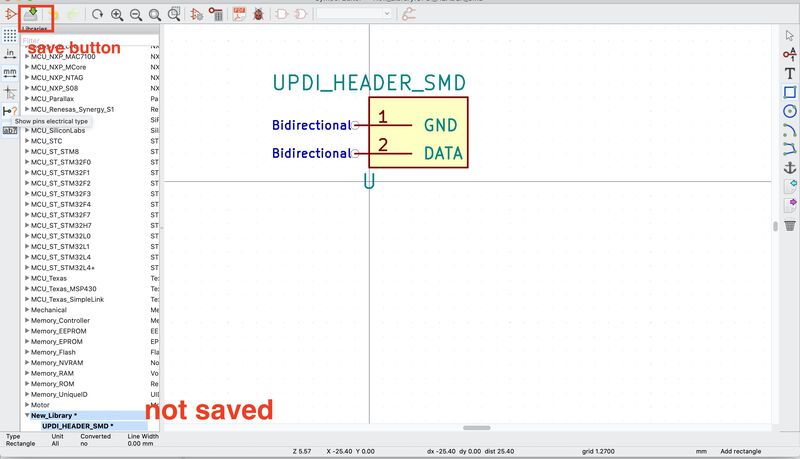
The asterisk marks next to the name of the library and symbol mean that they are unsaved. Save them by clicking the Save all changes button on the top left
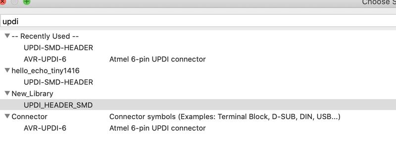
If you go back to the schematic window and search for the new component name, you will see that it's there
Once adding a symbol is done successfully, you have to add a footprint
How to create a footprint
Go back to the KiCad main window
Go to Tools > Edit PCB Footprints. This will open a Footprint Editor window
Then, go to File > New Library and give the same name as the name of the library you created for the symbol. (I think you can skip this step. But it makes finding a footprint easier later if you do it this way.) Like before, don't add the footprint to the existing library that you download from GitHub, because it might cause a problem syncing with the original library later
Select either Global or Project depending on your situation
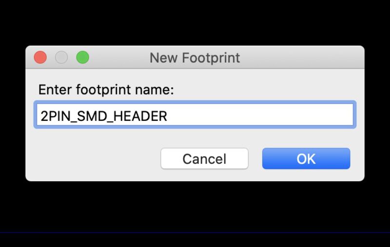
Go to File > New footprint and give a name to the footprint
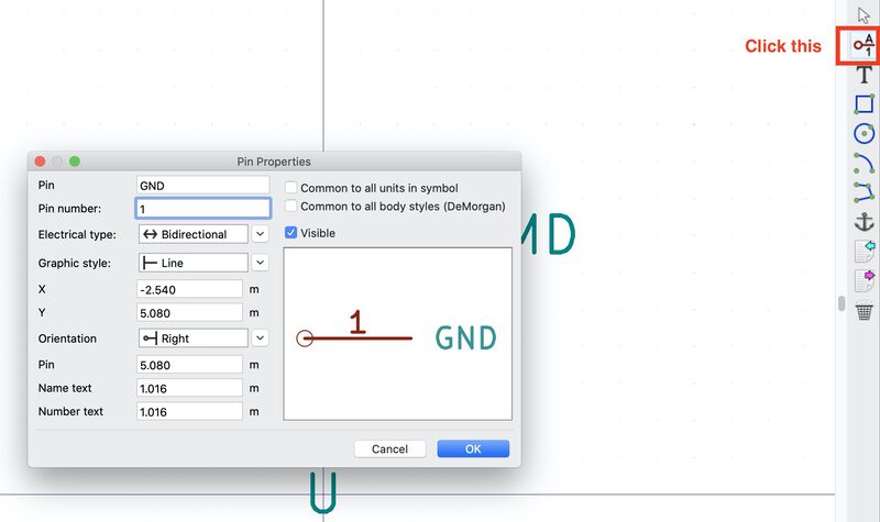
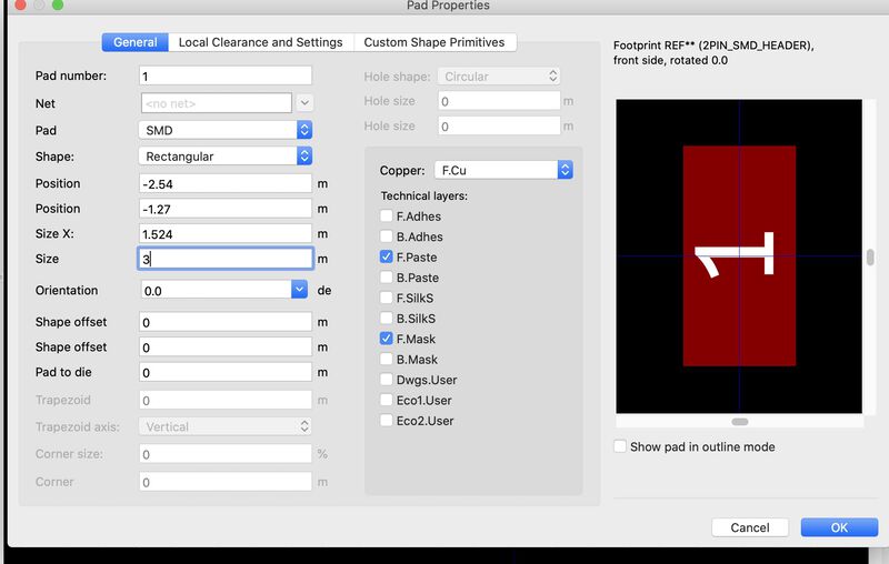
Then, add a component the footprint needs. In my case, I added pads for the pins from Place > Pad
Right click the component and click Properties. I set the pin to SMD type, shape to Rectangular and size to 3mm
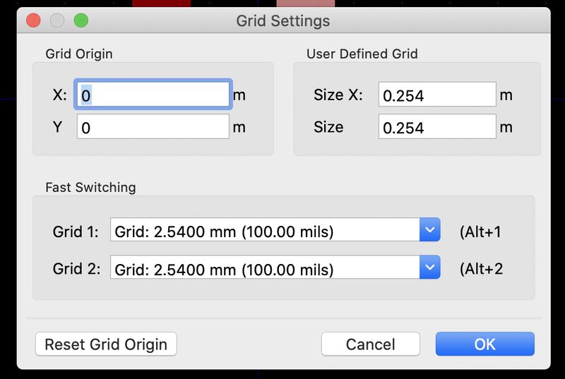
One thing I forgot was to set the distance between pins. The 2-pin header I used has a distance of 2.54mm. You can change it from Grid settings. Go to View > Grid Settings and choose the grid option
Save the file when it's done
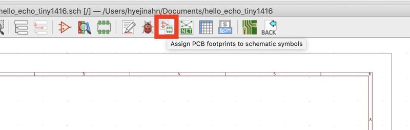
Go back to the Eeschema window and add the symbol you created
Click the Assign PCB footprints button
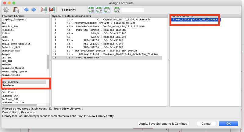
Click Annotate when the annotate popup shows up. There, you will see the list of footprints. Select the symbol you want to assign a footprint to, and select the library you created from the left panel. Then, you will see the footprint you created.
Individual Assignment
1. Make an ATtiny1614 board
This week, I made a lot of mistakes along the way to making a hello echo board with ATtiny1614. Sometimes I was frustrated by the problems I ran into, but eventually I learned a lot from them.
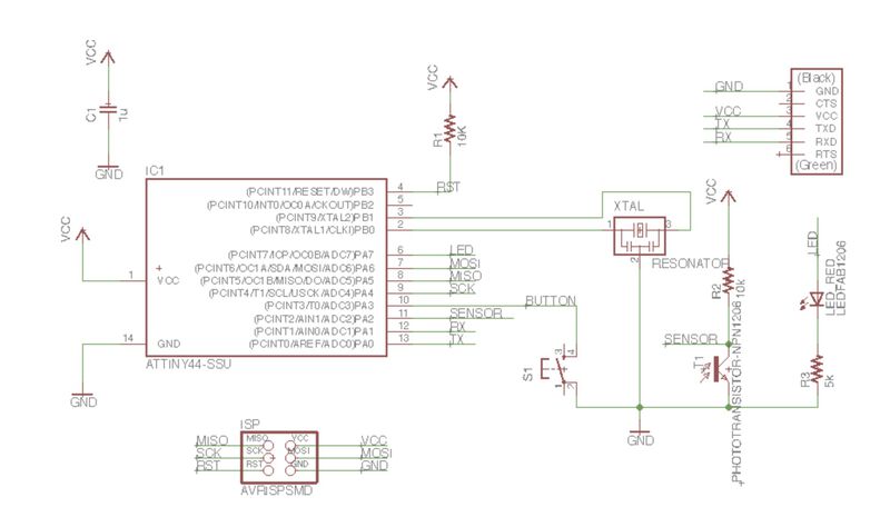
ATtiny 44 schema
Henk sent me a similar schema that was made with the ATtiny44, which helped me to grasp where to start. However, there were some changes I needed to make. For example, there was an external resonator in the ATtiny44 schema, but I didn't have to add it since ATtiny1614 has a reliable clock inside. Also, the ATtiny44 board had an ISP header but I needed to add a UPDI header in my case.
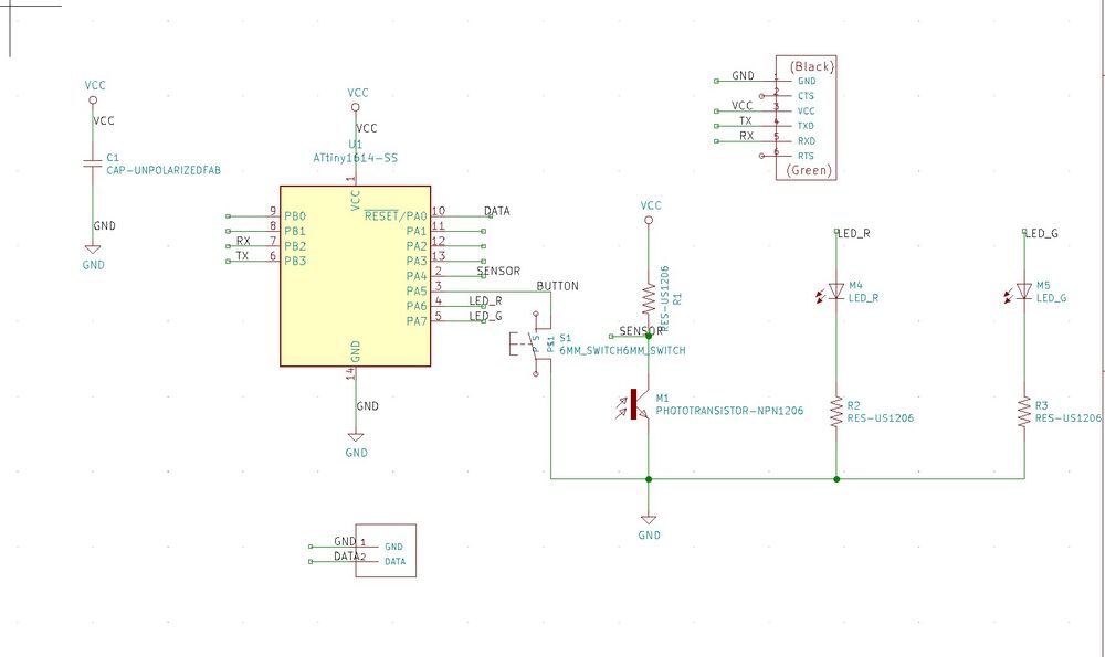
ATtiny1614 schema I drew
One thing that really confused me was how to connect the RX, TX cable. I remembered that I had to connect the RX port of the ATtiny1614 board to the TX of the FTDI board and vice versa. First, I checked the board to see which one was RX and TX.
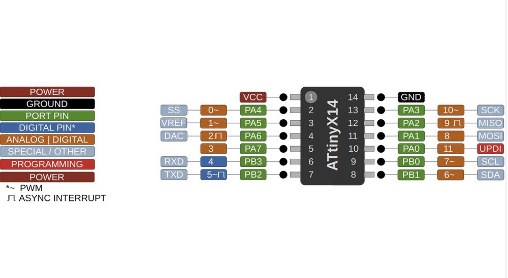
The PB3 on the ATtiny1614 was RX and PB2 was TX. So I connected the PB3 to the TX port of the FTDI, and PB2 to the RX port.
Issue 1. Couldn't find the 2-pin UPDI headers
When I draw a schema, I searched UPDI and found this symbol. But the UPDI headers I needed were supposed to have 2 pins, and mine had 6 pins. I used this since I didn't have any other symbol in my library and I thought it's going to be okay. But this turned out to be not working for two reasons.
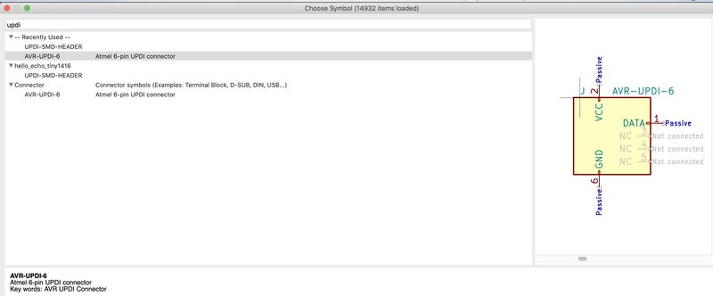
Reason 1. I needed a 2-pin header, not a 6-pin one
Reason 2. I needed a SMD component, not a THT one
I asked Henk and he said I need to create a symbol and footprint for the 2-pin if it didn't exist in the library. I googled how to do it and found these YouTube videos that helped a lot. But the videos were a little bit outdated so I had to figure out some of the steps by myself.
| YouTube | How I did | |
|---|---|---|
| schematic symbol | Create a symbol | How I created a schematic symbol |
| footprint | Create a footprint | How I created a footprint |
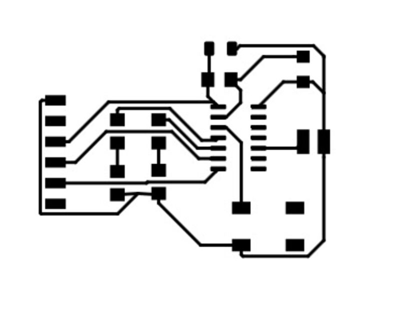
After adding a new symbol and footprint, I was able to do the rest of the workflow. These are the trace and the outline files.

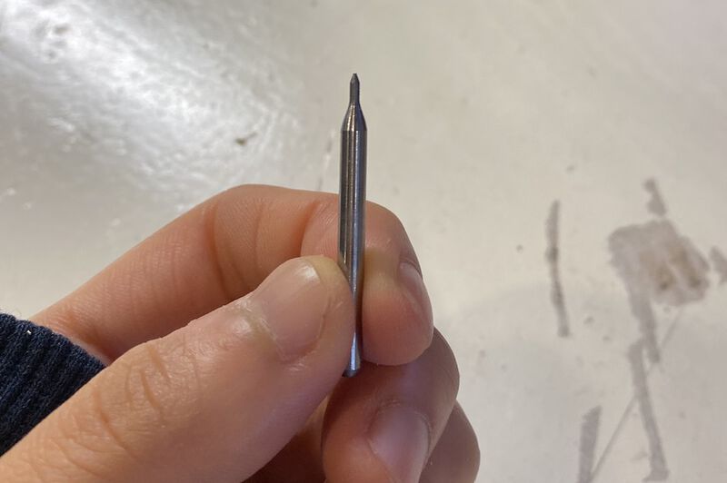
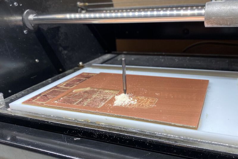
Issue 2. Mistakes during the milling process
First, I imported the trace SVG file into the mods and clicked the invert button.
But I forgot to change the flow control settings to RTSCTS and started the machine. The milling machine acted weirdly and the drillbit broke. I asked Henk about it and it turned out that I set the flow control to the wrong settings.
I fixed the settings and the trace file was milled perfectly.
Issue 3. Bad PCB design
After milling the trace, I imported the outline file and started the milling process. And the third problem occured.
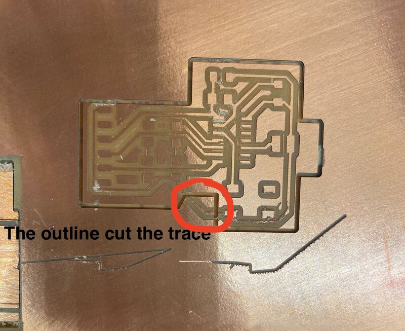
The outline cut across the trace. I probably made a mistake while I was drawing the outline in KiCad. I was going to mill another board, but Henk suggested me to use a wire to connect the disconnected parts. So I cut a wire and used it to bridge them. I thought that's the only problem but there was another unforseen problem.
When I placed the 2-pin UPDI header, I didn't think about the direction of the component and I placed it vertically. And when I tried to solder it, I realized that I should've placed it horizontally. I couldn't solder the way I designed, because the switch was blocking part of the way where the header part should be. I had to rotate a bit to place the header and it looked weird.
Issue 4. Traces too close
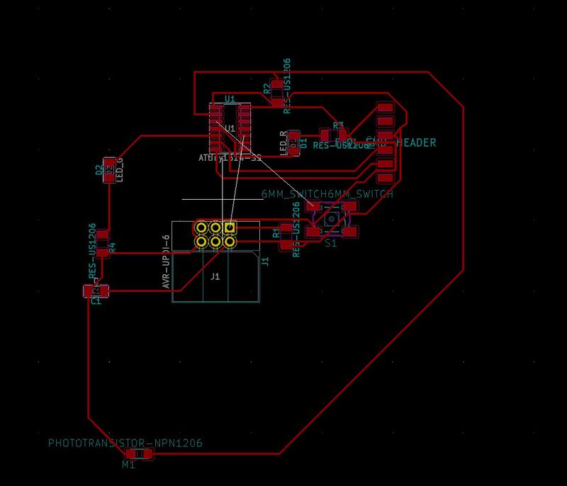
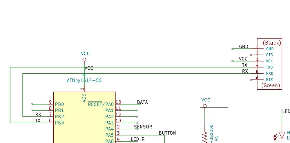
This is the second design of the ATtiny1614 board.
After milling and soldering it, I found that the small part of the two traces on the right side were connected. I tried to disconnect them with a cutter but I ended up destroying the trace around it. There are two lessons I learned. The first one is not to put traces too close together, and the second one is not to place traces under the pin connector.
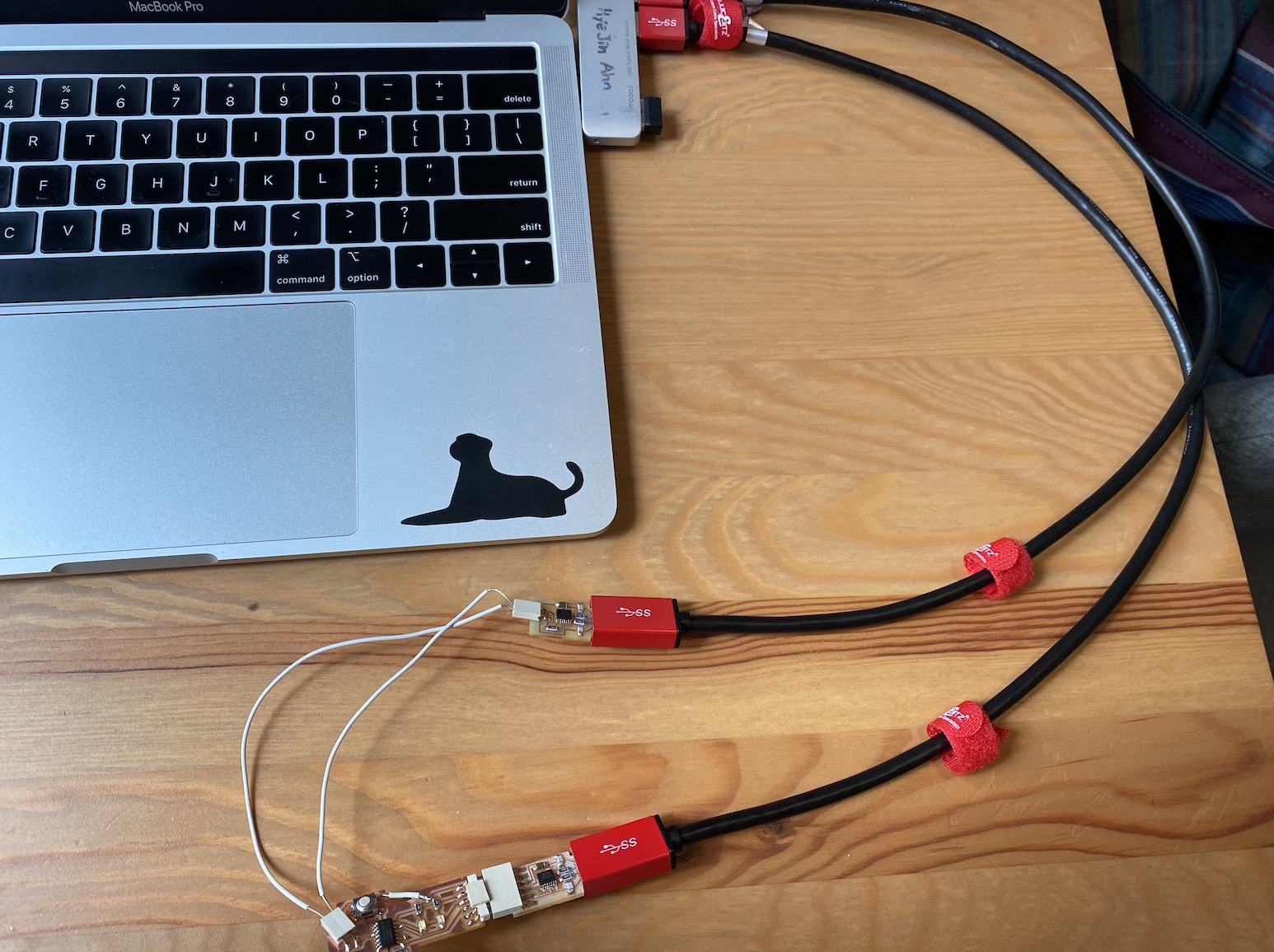
2. Program the board through a UPDI cable
To program the ATtiny1614 board, I needed a UPDI and FTDI board. I had an FTDI board that I made two weeks ago, and I borrowed Henk's FTDI board to test it.
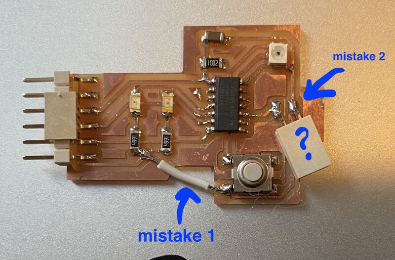
I connected them to my computer like in the photo below. I soldered a 2-pin connector on my board, instead of a 2-pin header, so I couldn't connect it with the UPDI board. I had to use 2 wires to connect 2 connectors.
I was worried that it might not work. Fortunately, the green LED turned on as soon as I connected the UPDI board with it. That was a big relief.
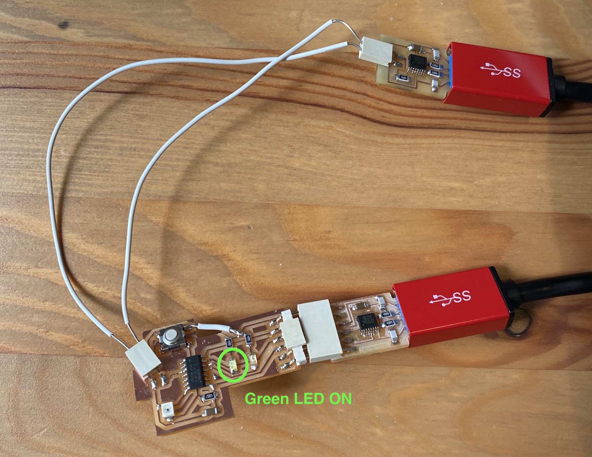
But after a long while, I realized that the green light wasn't supposed to light up. This was because of the connection between two paths that weren't supposed to be connected.
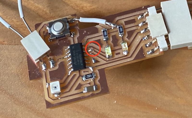
I couldn't notice it with my bare eyes. But I used a multimeter to figure out why the green LED was on, and I found that those two paths were slightly connected because of the solder. I scraped it with a cutter and the light turned off.
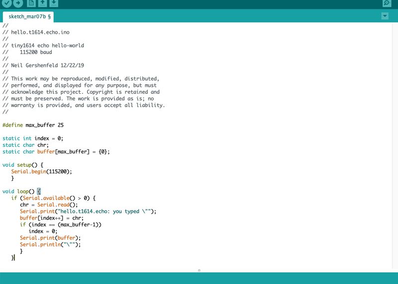
Then, I went to this link and downloaded the hello eco Arduino code. I copied and pasted the code into the Arduino IDE.
I tried to follow this video instruction, but I couldn't find the ATtiny1614 board.
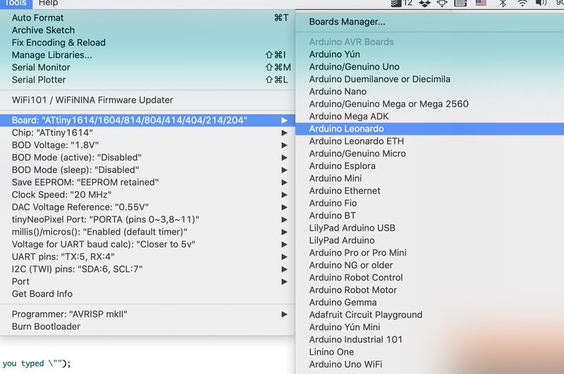
I once again googled and found how to add a board library to Arduino IDE.
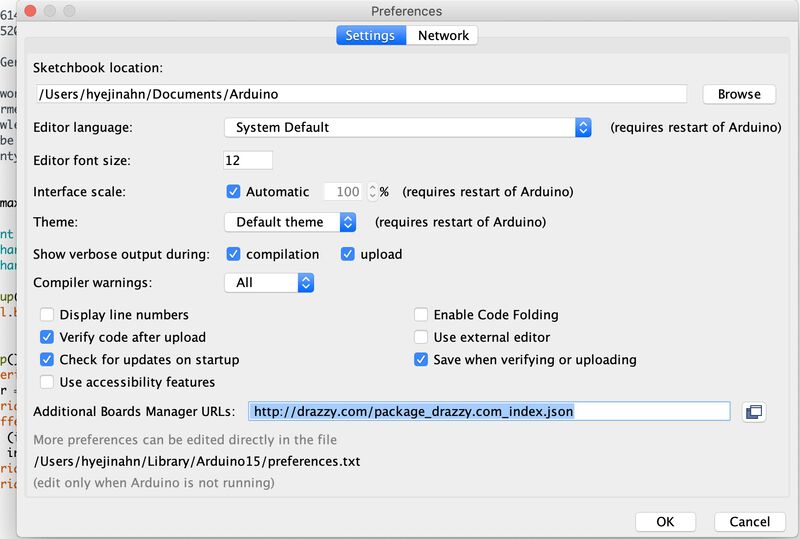
First, I went to File > Preferences and added this url (http://drazzy.com/package_drazzy.com_index.json) to the Additional Board Manager URLs field.
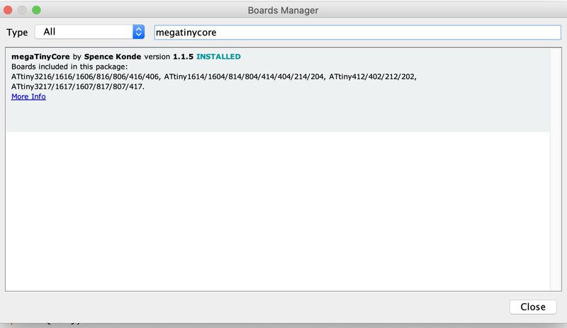
Then, I went to Tools > Board > Boards Manager. In the popup, I searched for megatinycore and installed this package.
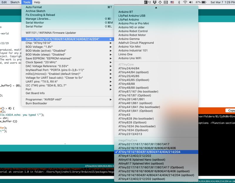
After doing all these, I was able to find the ATtiny1614 option from the list. And I set the other settings like the video tutorial.
I clicked the verify button on the top left, and it created a lot of files including a hex file.
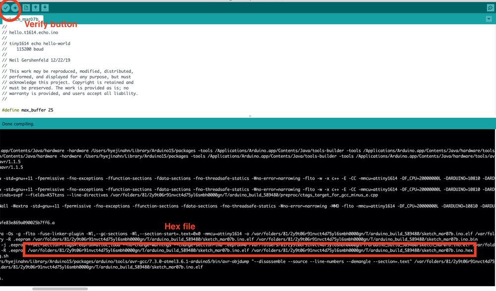
Updated: This was how I got the hex file, but our global evaluator Yuichi told me a better way.
I copied the path of the hex file and went to the terminal. Before programming the board, I needed to install some programs.
pip install https://github.com/mraardvark/pyupdi/archive/master.zip # to install Python UPDI driver for programming (https://github.com/mraardvark/pyupdi)
pip3 install intelhex pylint pyserial
Then, I needed to find the USB port that the UPDI was connected to.
ls /dev/*usb*
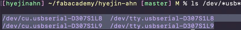
I found two ports but I wasn't sure which one was UPID and FTDI. So I just ran the code twice to see if either of them worked. I edited this example code (python3 pyupdi.py -d your_processor -c your_port -b your_baud_rate -f your_hex -v).
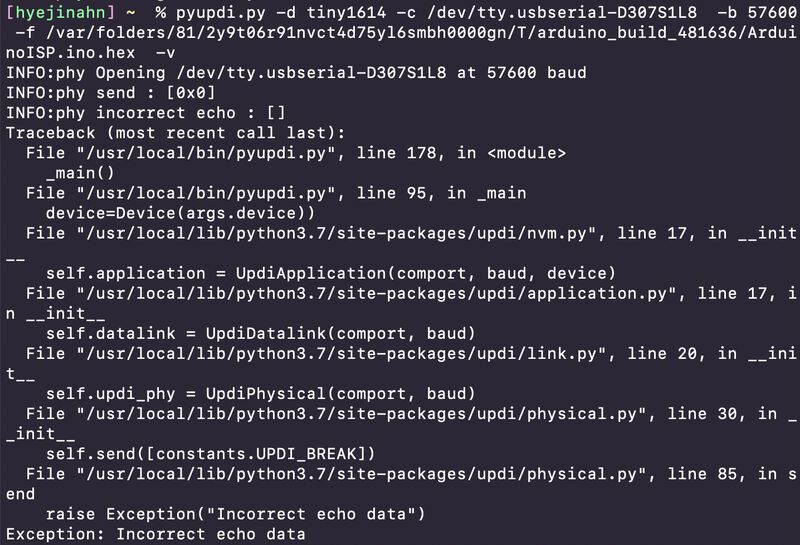
pyupdi.py -d tiny1614 -c /dev/tty.usbserial-D307S1L8 -b 57600 -f /var/folders/81/2y9t06r91nvct4d75yl6smbh0000gn/T/arduino_build_481636/ArduinoISP.ino.hex -v # with tty.usbserial-D307S1L8


pyupdi.py -d tiny1614 -c /dev/tty.usbserial-D307S1L9 -b 57600 -f /var/folders/81/2y9t06r91nvct4d75yl6smbh0000gn/T/arduino_build_481636/ArduinoISP.ino.hex -v # with tty.usbserial-D307S1L9
Both didn't work. (frustrated)
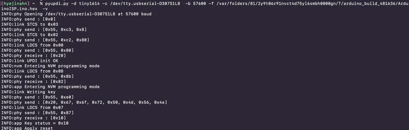
Henk told me to swap the wires between the UPDI and the board. I swapped them and ran the code again. Then, it worked! It spat out many lines of error. It turned out the UPDI cable was connected to tty.usbserial-D307S1L8 and the FTDI was connected to tty.usbserial-D307S1L9.
raise Exception("Failed to chip erase using key")
Sometimes I got this error message. In my case, it could be fixed simply by plugging off the USB hub from my computer and plugging back on.
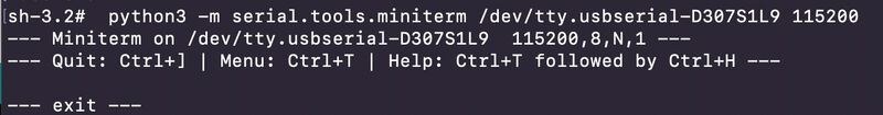
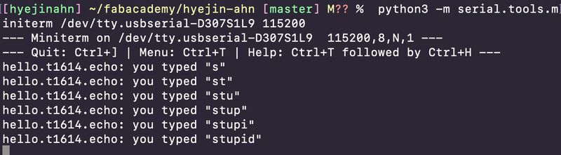
3. Communicate with the board through an FTDI cable
After downloading the program, I tried to communicate with the board using the FTDI cable. I used the tty.usbserial-D307S1L9 port when I ran the code below.
python3 -m serial.tools.list_ports # shows the list connected serial
python3 -m serial.tools.miniterm /dev/tty.usbserial-D307S1L9 115200 # communicate with the FTDI port
Issue 5. No echo coming back
When I ran the code and typed something, nothing showed up. I couldn't type anything on the terminal. Henk said RX and TX in my board might need to be swapped. Before I swapped the RX and TX, I tried to debug it.
I couldn't see anything that was going on and I found that I could add a flag to print debugging information.
python3 -m serial.tools.miniterm -f debug /dev/tty.usbserial-D307S1L9 115200 # add debug filter (https://pyserial.readthedocs.io/en/latest/tools.html)
This just showed me what I typed (or sent), but I couldn't see any response from the board.

What I tried
I thought it might be because of wrong RX, TX connection. So I swapped the TX and RX connection and tried running the echo hello world code - FAILED
I updated the code to light up the red LED - FAILED
I swapped the RX, TX connection back and tried to run another code (Light up the red LED) - FAILED
But nothing worked. Then, I got an idea: The problem might be the way my board and the FTDI are connected.
This was right. I checked the FTDI board and I found that the way it was connected to my board was wrong. That was the reason why I couldn't communicate with my board. After I flipped my board and connected it with the FTDI cable, the code worked like a charm.
When it first worked, I was a little bit frustrated. Because I spent 2 days fixing this, and it turned out to be a very simple reason. (maybe it looked simple now)

But eventually, I was so happy that I figured it out. Also if something like this happens again, now I know where to check first.
Issue 6. Weird behavior
The next morning, when I tried to download the echo hello world program into my board again, I started getting this error.
Traceback (most recent call last):
  File "/usr/local/bin/pyupdi.py", line 178, in
    _main()
  File "/usr/local/bin/pyupdi.py", line 105, in _main
    if not _process(nvm, args):
  File "/usr/local/bin/pyupdi.py", line 130, in _process
    return _flash_file(nvm, args.flash)
  File "/usr/local/bin/pyupdi.py", line 143, in _flash_file
    nvm.write_flash(start_address, data)
  File "/usr/local/lib/python3.7/site-packages/updi/nvm.py", line 106, in write_flash
    self.application.write_nvm(address, page)
  File "/usr/local/lib/python3.7/site-packages/updi/application.py", line 269, in write_nvm
    self.write_data_words(address, data)
  File "/usr/local/lib/python3.7/site-packages/updi/application.py", line 222, in write_data_words
    return self.datalink.st_ptr_inc16(data)
  File "/usr/local/lib/python3.7/site-packages/updi/link.py", line 187, in st_ptr_inc16
    self.updi_phy.send(data) # No response expected.
  File "/usr/local/lib/python3.7/site-packages/updi/physical.py", line 85, in send
    raise Exception("Incorrect echo data")
Exception: Incorrect echo data
INFO:phy Closing /dev/tty.usbserial-D307S1L8
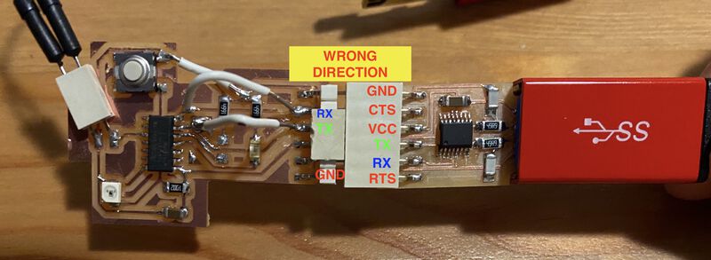
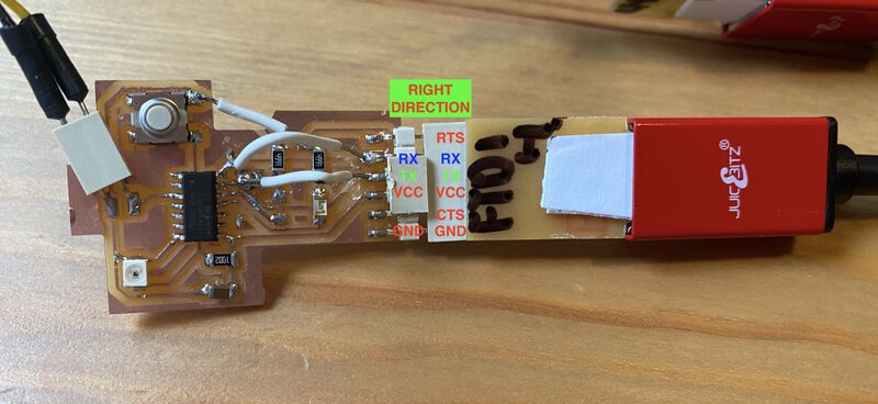
I panicked because it worked last night and it wasn't working anymore. The connection between FTDI cable and my board was like this.
I flipped it over as it used to be and downloaded the program just in case. And it worked! But I had to flip it over to the right direction to communicate with the board again.
Basically, I had to connect in the so-called wrong direction to download the program to the board, and the right direction to communicate with the board. I found it so weird and I tried to find the reason but I couldn't find it.
Update: This problem was fixed on the new board. It was probably because of a wrong connection on the board.
4. Control an LED
I also wanted to play with an LED and a button on the board. I initially had two LEDs, one red and one green. But I burned the green one. So I tested with the red one, and a new issue showed up.
Issue 7. Wrong pin number
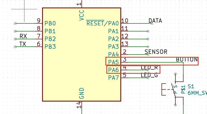
As you can see in the photo above, the red LED was connected to pin 4, and the button was connected to pin 3.
int ledPin = 4;
int buttonPin = 3;
int buttonState = 0;
I first wrote a code like this but it didn't work. The led light didn't turn on and the switch didn't seem like it was responding. So I looked at the Arduino ATtiny board library source code and found this part where all the pins were initialized.
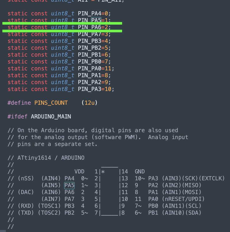
/Users/hyejinahn/Library/Arduino15/packages/megaTinyCore/hardware/megaavr/1.1.5/variants/txy4/pins_arduino.h
Updated: You can also find these pin numbers from the megatinycore library.
I was using the wrong pin numbers. The pin numbers I used were the ones for the ATtiny1614 board. Instead, I had to look at the code and see how those numbers were initialized in the library. For example, the red LED was connected to PA6 which was defined as 2 in the library. And the button was connected to PA5 which was defined as 1. I updated the variables like below, and it worked.
int ledPin = 2;  // This is the pin of the ATtiny1614 connected to the REDled
int buttonPin = 1; // This is the pin of the ATtiny1614 connected to the button
int buttonState = 0;


void setup() {
  pinMode(ledPin, OUTPUT);
  pinMode(buttonPin, INPUT_PULLUP);
  Serial.begin(115200);
}

void loop() {
  buttonState = digitalRead(buttonPin);
  if (buttonState == LOW) {
    Serial.print("BUTTON ON"); // Since it's a pull up botton, the LED is on when the buttonState is LOW
    Serial.println("\"");
    digitalWrite(ledPin, HIGH);
    delay (50);
    digitalWrite(ledPin, LOW);
    delay (50);
  }
  else {
    Serial.print("BUTTON OFF");
    Serial.println("\"");
    digitalWrite(ledPin, LOW); // If the button is not pressed the RED light is off.

  }
}
Other than the issues above, I made more small mistakes. I almost broke another drillbit while milling the outline and torn the copper trace while trying to detach the headers.
A drill bit got stuck on the board
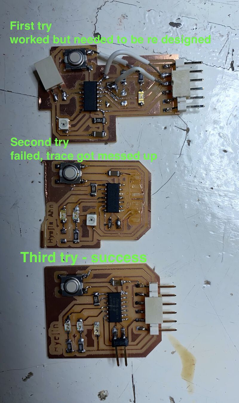
I ended up making three ATtiny1614 board, and finally the last one worked.
Henk said if I didn't make a mistake, I wouldn't learn anything. I guess I learned A LOT this week.
5. Make a UPDI
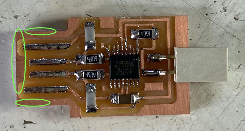
To update programs onto the ATtiny1614 board, I needed a UPDI board. So far, I've been using Henk's UPDI board. Since I had some time left this week, I decided to make a UPDI board as well.
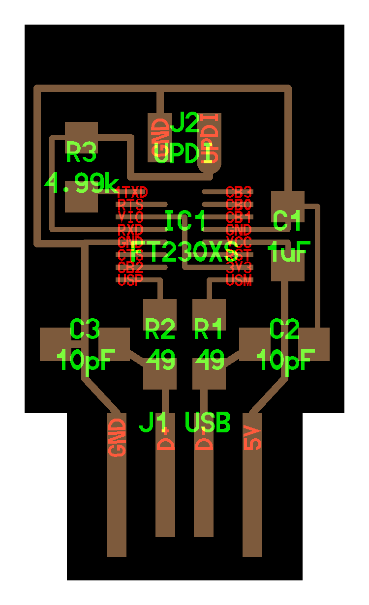
After milling and soldering, I connected my ATtiny1614 board, but my computer gave me this message and refused to connect with it.
I didn't know what the problem was at first. Henk told me that it might be because of a short on the circuit.
I should’ve removed the copper layers around the USB connector but I forgot. That caused a short in the board and my computer refused to connect to it because of that. After scraping that part out, which was a lot of work, the board was connected successfully and was able to program the ATtiny1614 board.
6. Summary
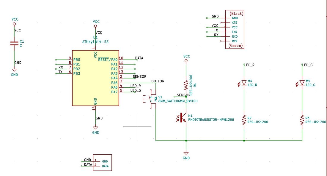
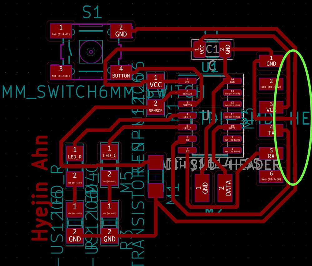
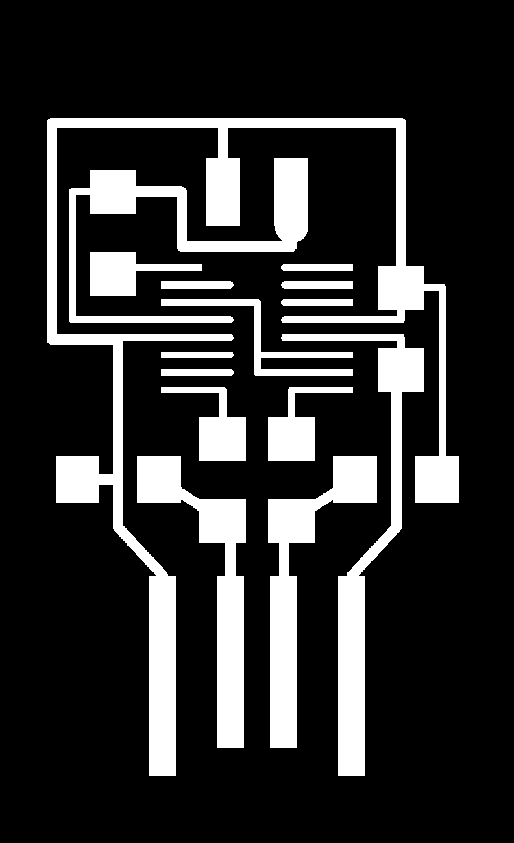
Final schema
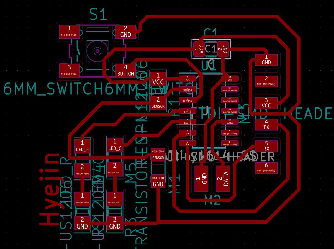
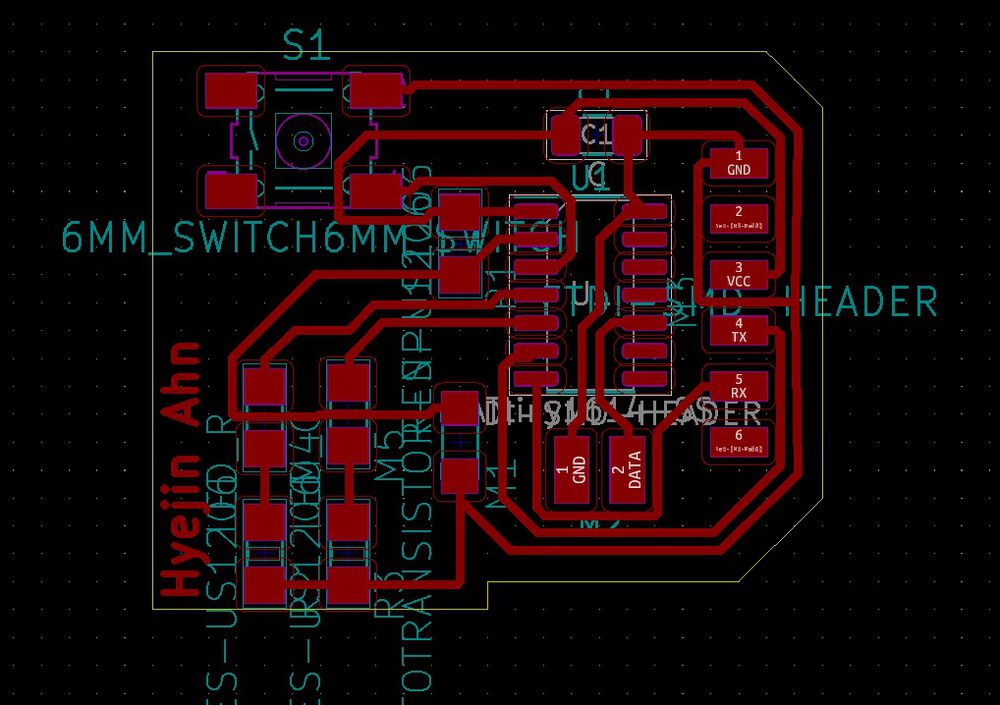
Final PCB route
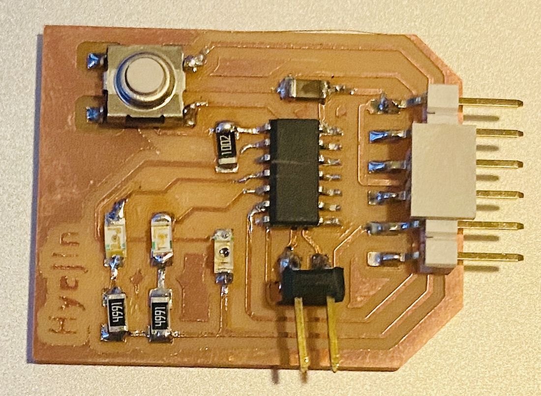
Final board
This is the video of running the blink code I wrote. When I click the button, BUTTON ON message shows up and the LED starts blinking. By the way, I thought I put a red LED but it turned out to be a green :P
Group assignment
This week's group assignment(group assignment documentation) was to test equipment in our lab to observe the operation of a microcontroller circuit board.
First, Henk showed us how to use a logic analyzer. The one Henk used was Saleae Logic 16. With this tool, we could see the 8 bits of zeros and ones for each input. I was impressed that we could really read the digital input and output this way.
After Henk showed us more how to use an oscilloscope and a power supply, our group tested it out on our own. We powered an ATtiny board with the power supply and tested it with the oscilloscope. We clicked the button on the board and checked the voltage between the VCC and an LED. The details are written on the group assignment.
I still haven't really figured out how to use the oscilloscope or how I could utilize it. But the logic analyzer seemed really useful, especially when debugging a board.