About Week 6
My Electronics Design Exercise...
This week assignment was about Electronics Design, in particular starting from the echo hello-world board:
- 1. add a button and LED to the echo hello-world board,
- 2. check the design rules,
- 3. make it.
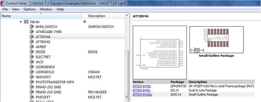
The first step was design the board. To do this we used Eagle. EAGLE (Easily Applicable Graphical Layout Editor) is a flexible and expandable EDA schematic capture, PCB layout, autorouter and CAM program. EAGLE is popular among hobbyists because of its freeware license and rich availability of component libraries on the web. The main feature of Eagle is that you can design from two perspectives: the schematic view, that is a drawing representing a circuit by using symbols to represent real-world electronic components, and the board layout that shows how the electrical componets and traces will be laid out on the board.
First of all I downloaded the Eagle installer , I've installed the freeware version and downloaded the eagle project of helloEcho example
Before starting I followed suggestions from Fab Academy Eagle Tutorial
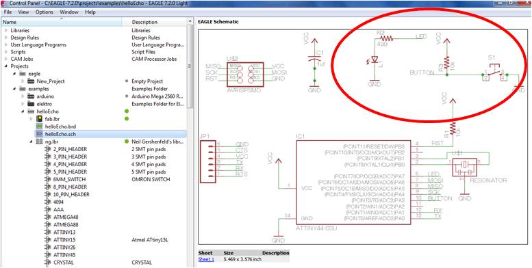
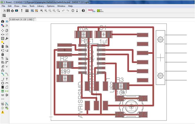
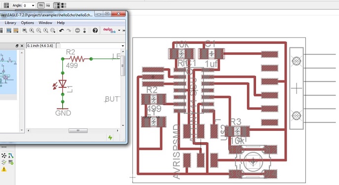
Once imported the HelloEcho I started to add the need components not yet inserted into the schematic
The Led, the button and related resistors were connected to ATTINY44, to pin 6 and 10 respectively. I calculated the current limiting resistor by using the web tool http://led.linear1.org/1led.wiz
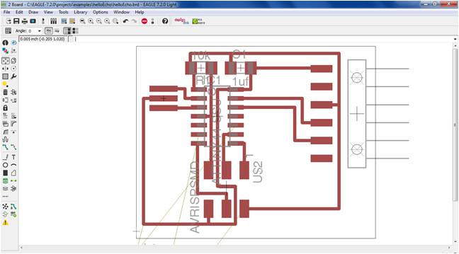
After this I switched to the board view and the inserted component were located down on the left and their traces not displayed. I reduced the zoom an I tried to allocate them by using the autoroute function, but without success. After several temptatives, I realized that the problem was that starting from the example many of the components are just displaced reducing a lot the available space. So I decided to manualy arrange the components and the traces.
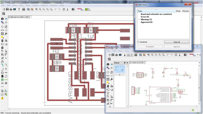
I've checked for errors, but only warnings.
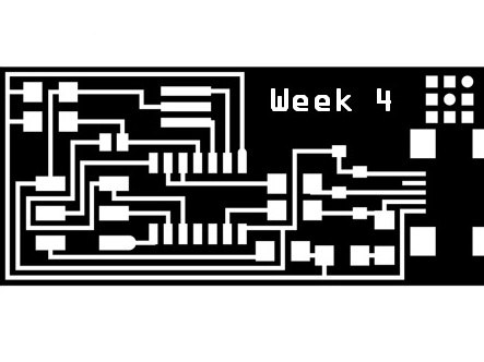
The next step was to prepare the board for printing. I've deselected some levels, changed the backgroundand exported as monochrome image with 1000 dpi of resolution
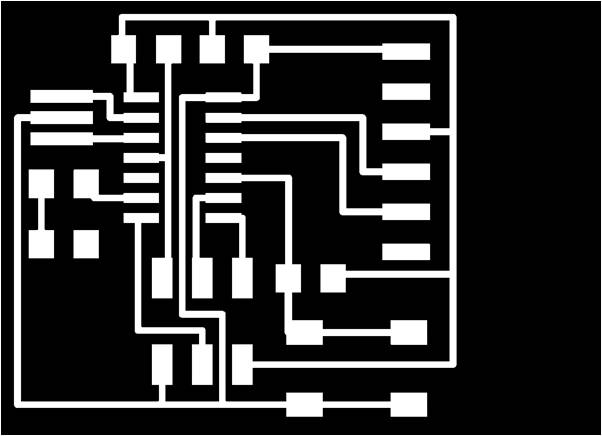
As done for my FabISP, I've imported the .png file into Inkscape, I vectorized it and I added text and a red square
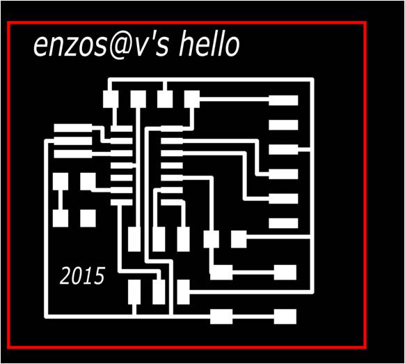
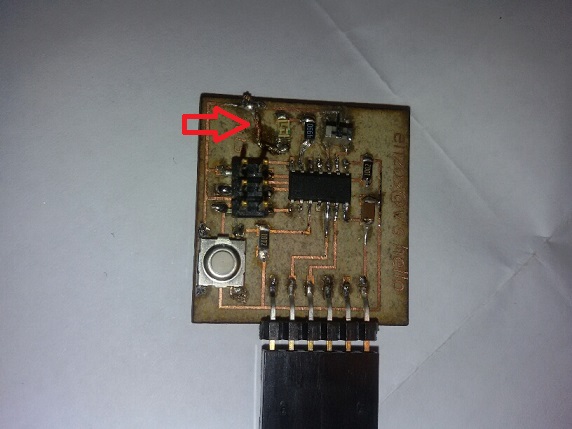
ready for engraving and cutting. Unfortunately after the engraving I found an error in my board:
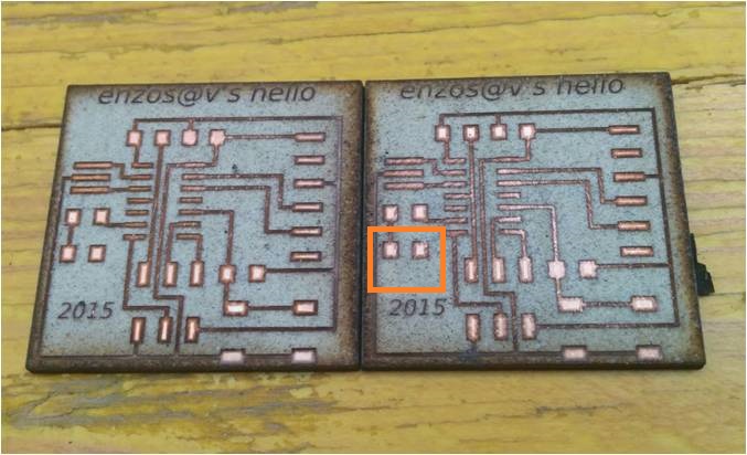
The path from the led cathode and GND was missing, and I did not notice this during the export and check of board design. In order to check the error and solve it in eagle files I noticed that maybe the error was the missing junction between led and ground in schematic. I corrected it and saved the project.
Download the Eagle Project file
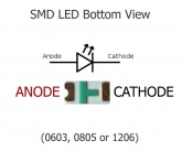
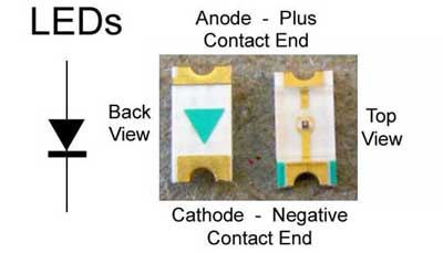
So I started to solder the components. About Led in order to identify anode and cathode I checked the symbols:
About the board I decide to solve the problem during the components soldering by making an emergency junction. For the
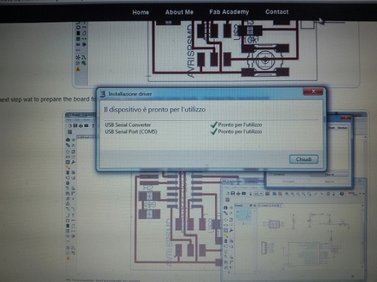
Once finished, with crossed fingers, I connected the FTDI cable with my PC and my helloboard for a smoke test: seems all OK! In the next week exercise I will check if the board is able to be programmed.