Caution! José Figueroa at FabAcademy 2013
Weekly report of my work at FabLab Barcelona
This is week 6, which means we have done roughly a third of what the FabAcademy is about. Amazing how time passes by. We were introduced to a lot of topics in only one hour and a half. Ohm's law, Kirchorff's laws, schematics, design of PCBs. A lot of things I had to learn in many semesters, my classmates got a glimpse of in one class. For me it was a brilliant example of an "introductory" class. And I always manage to learn something new, which in this case is the usage of Eagle CAD to design electrical schematics and PCBs.
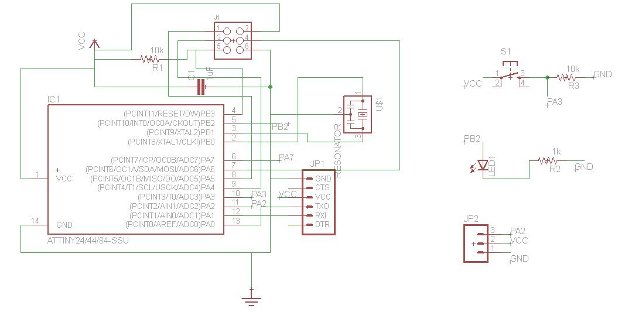
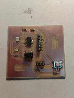
This week's asignment was to take a board already made and to modify it by adding an LED and a button. I did so using Eagle CAD. Each component needs to have a resistance for different purpose. An LED needs a resistor to limit the current flowing through it. A button needs a pull-up or pull-down resistor. In my case I use a pull-down resistor in order to make reference to ground voltage level whenever the button is in the off position. Besides these components, I also added a jumper with three terminals in order to have access to another pin of the microcontroller if needed. One terminal goes to the pin, another one is connected to the voltage source, and the other one is connected to ground. You can see below my schematic.
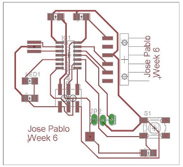
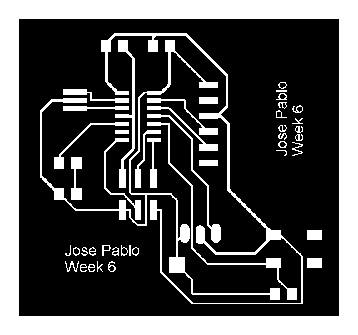
After doing the schematic, I proceeded to work on the PCB design. Eagle has a nice autorouting feature that, if it doesn't do the whole PCB routing, it does almost all of it. From there I got a nice start, and had only to work my way around a few traces. I did a first design which I intended to be the first of many iterations, but due to lack of time, it ended up being the final design. It's not as elegant as I intended, but it is functional.
