
This work is licensed under a Creative Commons Attribution-NonCommercial-ShareAlike 4.0 International License
Week 11: Input Devices
Apr 8, 2021Summary
This week's assignments
- Group assignment:
- Probe an input device(s)'s analog and digital signals ✔
- Document your work (in a group or individually) ✔
- Individual assignment:
- Measure something: add a sensor to a microcontroller board that you have designed and read it:
- Document what you learned from interfacing an input device(s) to microcontroller and how the physical property relates to the measured results ✔
- Document your design and fabrication process or link to previous examples ✔
- Explain the programming process/es you used ✔
- Explain problems and how you fixed them ✔
- Include original design files and source code ✔
- Include a ‘hero shot/video’ of your board ✔
Resources Used
- Software: KiCad, Adobe Illustrator, Arduino IDE
- Hardware: Roland SRM-20, Trotec Speedy 400 Flexx
Skills Gained
- KiCad, Basic Arduino programming, Accelerometer Usage, Reflow Soldering
My Weekly Schedule
The second half of the Fab Academy programme is designed to build on the previous weeks. You will be synthesising information and implementing skills that you were introduced to in the first half of the programme and encouraged to integrate these into your final project proposal.
Input Devices For My Final Project
Research: Acceleration, Orientation, Rotation
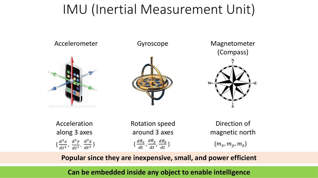
During the Global Lecture on Wednesday, Neil introduced to us various input devices that we could use for our final projects. Since my final project was about a posture assistive device, I knew that I would need to make an IMU input sensor to start woring towards the acceleration, orientation, and rotation measurement.
IMU stands for inertial measurement unit and was typically used for detecting the linear acceleration through the accelerometer(s) and rotational rate through the gyroscope(s). Some also included a magnetometer to measure the direction, strength, or relative change of a magnetic field at a particular location. Usually the data returned by iMUs are "fused" together and interpreted as roll, pitch, and yaw of the platform.
Research: ADXL343
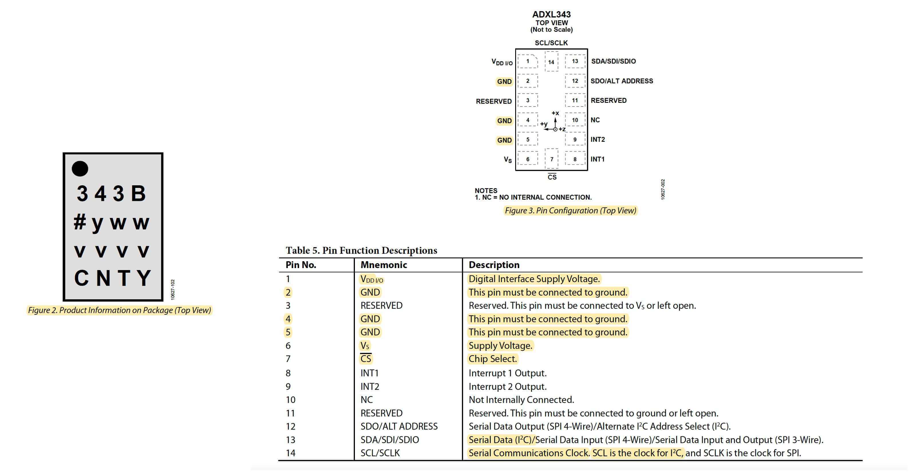
As our lab does not have a gyroscope at the moment, I started by doing some research on the ADXL343BCCZ accelerometer, and one important information is about the I2C communication portal.
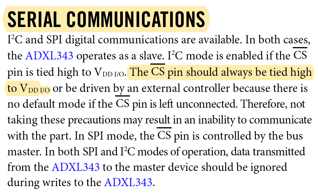
According to this arduino tutorial, the I2C involves two lines to send and receive data: a serial clock pin (SCL) and a a serial data pin (SDA). Because the I2C is for serial communication, the data is transferred bit by bit along a single wire (the SDA line). The Sparkfun resource also stated that the I2C bus drivers are "open drain", meaning that they can pull the corresponding signal line low, but cannot drive it high...Each signal line has a pull-up resistor on it, to restore the signal to high when no device is asserting it low. The resource suggested to start with 4.7kΩ resistor and adjust down if necessary. I have seen that Neil used three 10KΩ resistors on his board so I would follow his process.
Here is another information that I thought would be useful for PCB design (Source: ADXL343 datasheet).
PCB Design
Part 1: Creating the Schematic
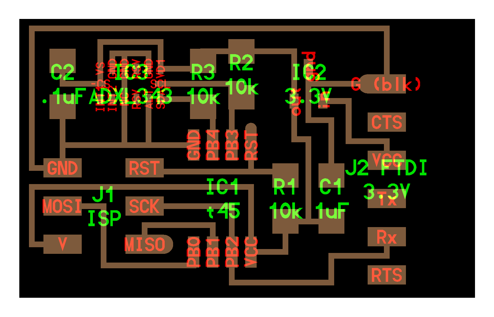
Apr 8, 2021For my final project, I would like to use the ADXL343 accelerometer as the input device, so I started by studying what components were included on Neil's board:
- Microcontroller: ATtiny45 - 1X
- Accelerometer: ADXL343 - 1X
- FTDI: 1x6 header - 1X
- ISP: 2x3 header - 1X
- Regulator - 1X (for 3.3V)
- Resistors - 3X 10KΩ
- Capacitors - 1X 0.1uF, and 1X 1uF
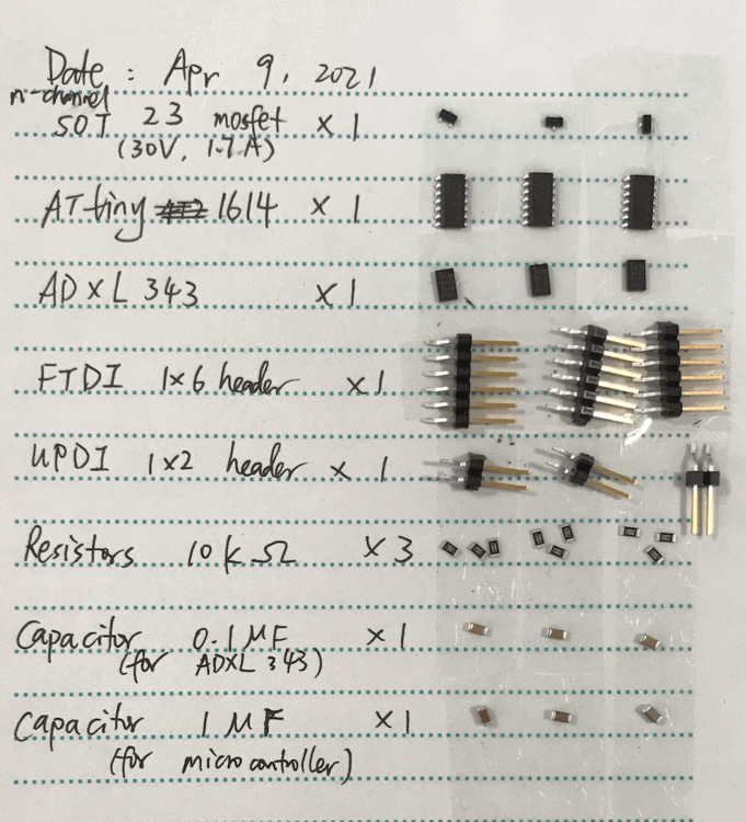
Since ATtiny45 doesn't work on the newer computers, I replaced the ATtiny45 with the ATtiny412, I also made sure to replace the ISP with the UPDI for that. Thus, the components that I needed for my board are as follows:
- Microcontroller: ATtiny412 (datasheet) (use "fab tiny" in search) - 1X
- Accelerometer: ADXL343 (datasheet) (use "fab acc" in search) - 1X
- FTDI: 1x6 header (use "fab ftdi" in search) - 1X
- UPDI: 1x2 header (use "fab updi" in search) - 1X
- Regulator: n-channel SOT23 MOSFET (datasheet) (use "fab reg" in search) - 1X (for 3.3V)
- Resistors (use "fab r" in search) - 3X 10KΩ
- Capacitors (use "fab c" in search) - 1X 0.1uF, and 1X 1uF
Although there were limited resources available on the routing for ATtiny412 and ADXL343, I still found these former students' sites helpful because they helped me to better understand the routing on Neil's board (1, 2, and 3).
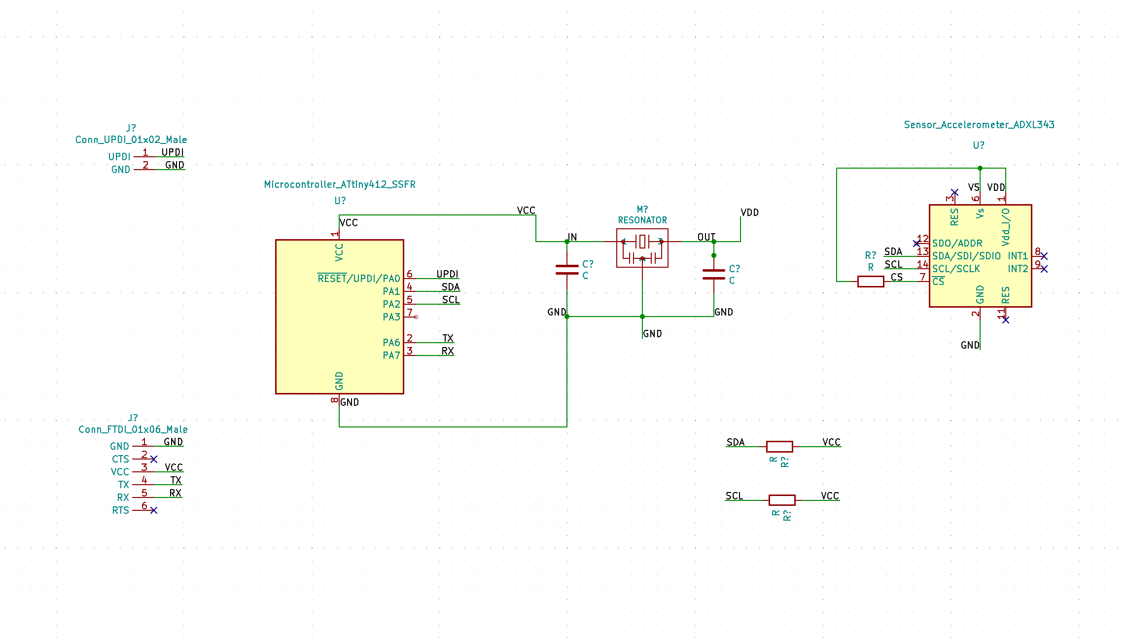
I decided to place my components in a similar fashion that I did for the hello.t412.echo board during the Electronics Design week (Image 1) to see if I can find any similarities or differences between the two. First, I connected the ATtiny412 with a capacitor to filter out the noise, I also placed the FTDI and UPDI to the left of the microcontroller (Image 2). After that, I saw what components were left and I figured that they would be important to the routing of the accelerometer (Image 3) - I found this trick extremely helpful for the later steps!
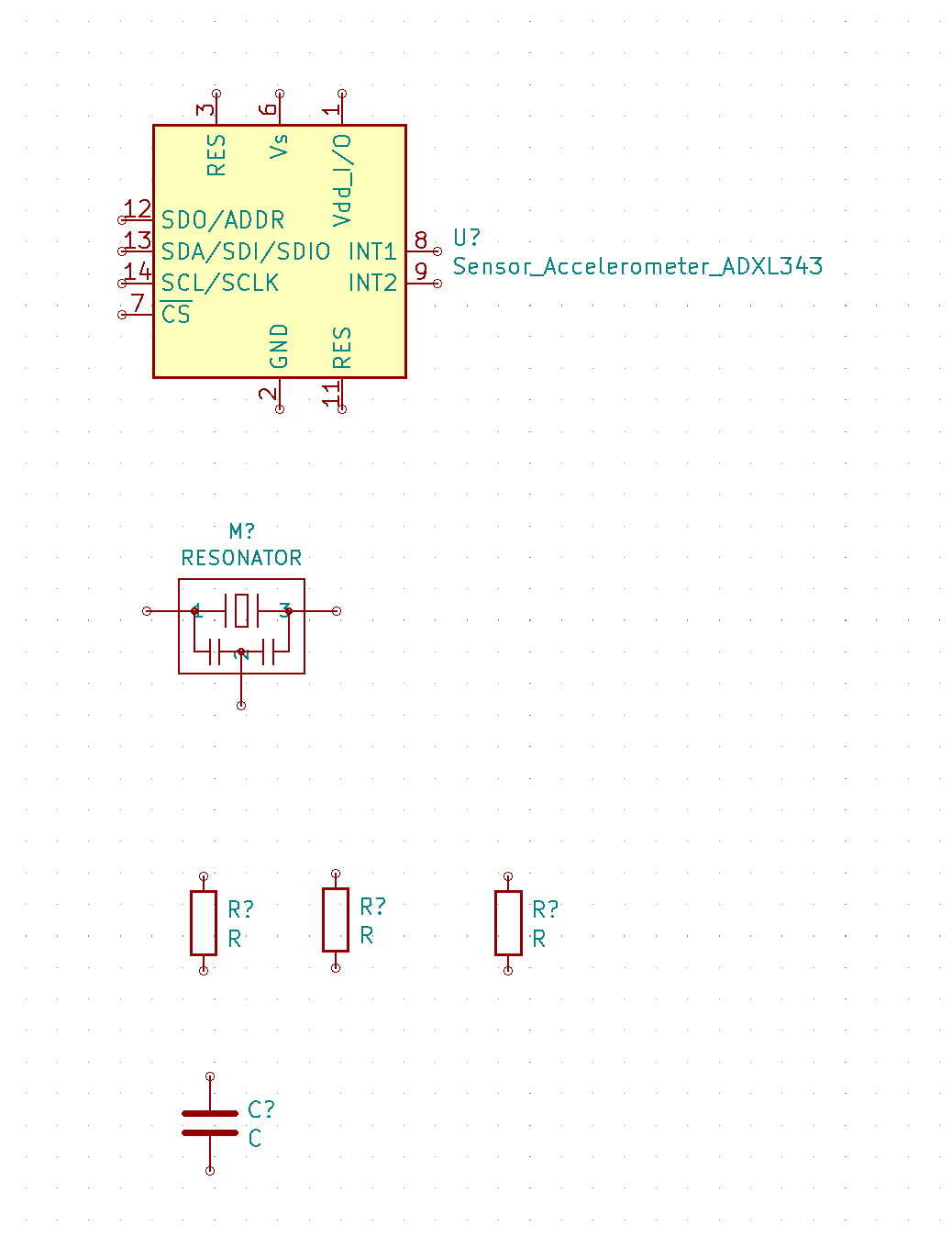
Reading from the ADXL343 datasheet, I knew that I wanted to use the I2C instead of the SPI for my board, so I referred to the pinout of the ADXL343 to cross out (use no connect in KiCad) the pins that I was not using first (i.e. crossing out the SDO pin). I saw that Neil didn't use the RES or the INT pins, so I crossed out mine also 😁!
Then I used the pinout for ATtiny412 to identify the digital pins. As shown in the image below, the UPDI, GND, and VCC pins were pre-determined, as I was not 100% certain about the usage of PA3, I decided to pick from the other options, which were PA1, PA2, PA6, and PA7. Since I wanted to use the default pins for TX (PA6) and RX (PA7), I set to use PA1 and PA2 of ATtiny412 (microcontroller) to connect the SDA and SCL pins of the ADXL343 (accelerometer), respectively.
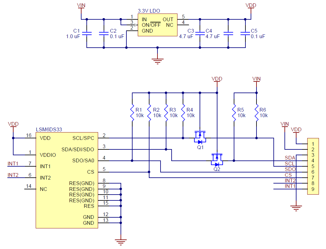
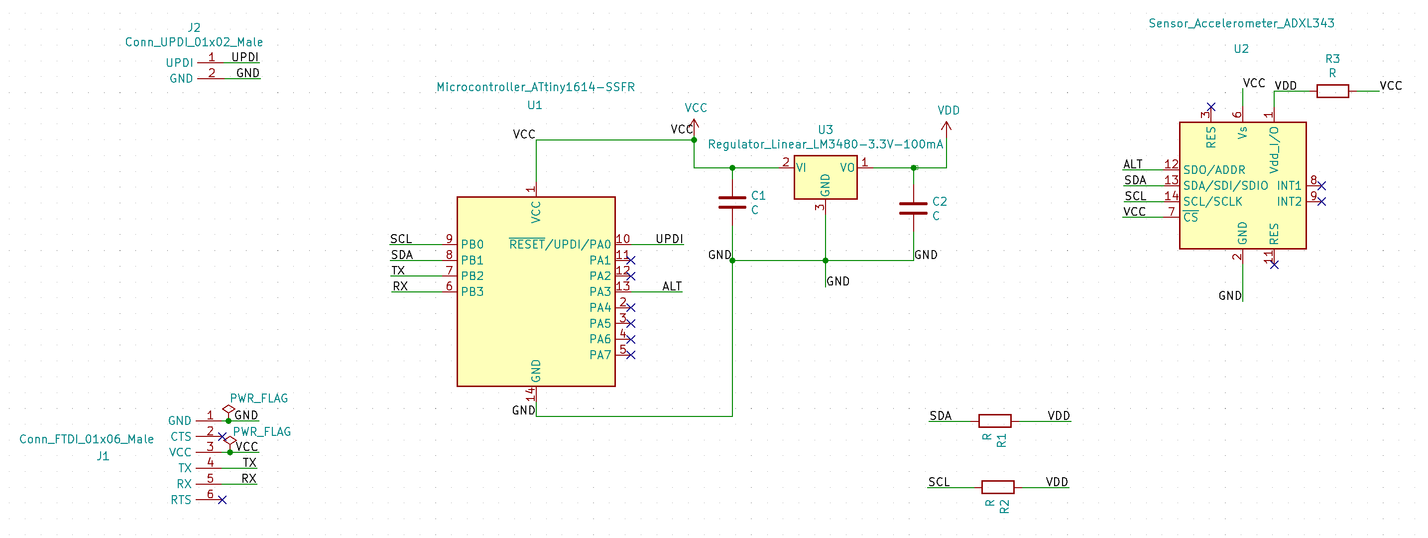
I then learned the basic wiring rule for the ADXL343 based on the schematic for the SM6DS33 breakout board. This was the IMU breakout board that Neil introduced during the Global Lecture on Wednesday, so I thought it could be a good starting point for me. From the schematic, I learned that I would need to connect the resistors to the CS, SDA and SCL pins. I also learned I should use the capcitors to filter out the noises in the regulator.
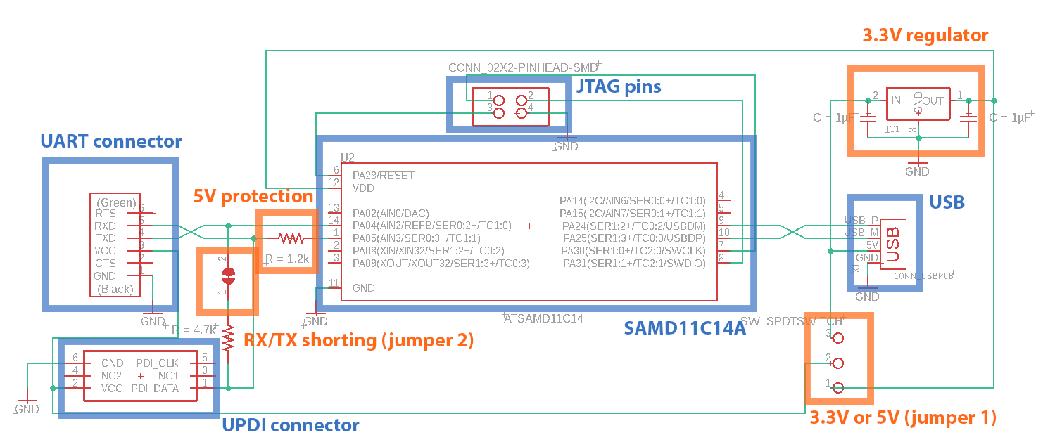
I recalled that I had seen a similar routing for the regulator from Quentin's SAMD11C schematic. There, he connected the same capacitor to the SAMD microcontroller and the regulator, so I decided to do the same for my ATtiny412_ADXL343 board.
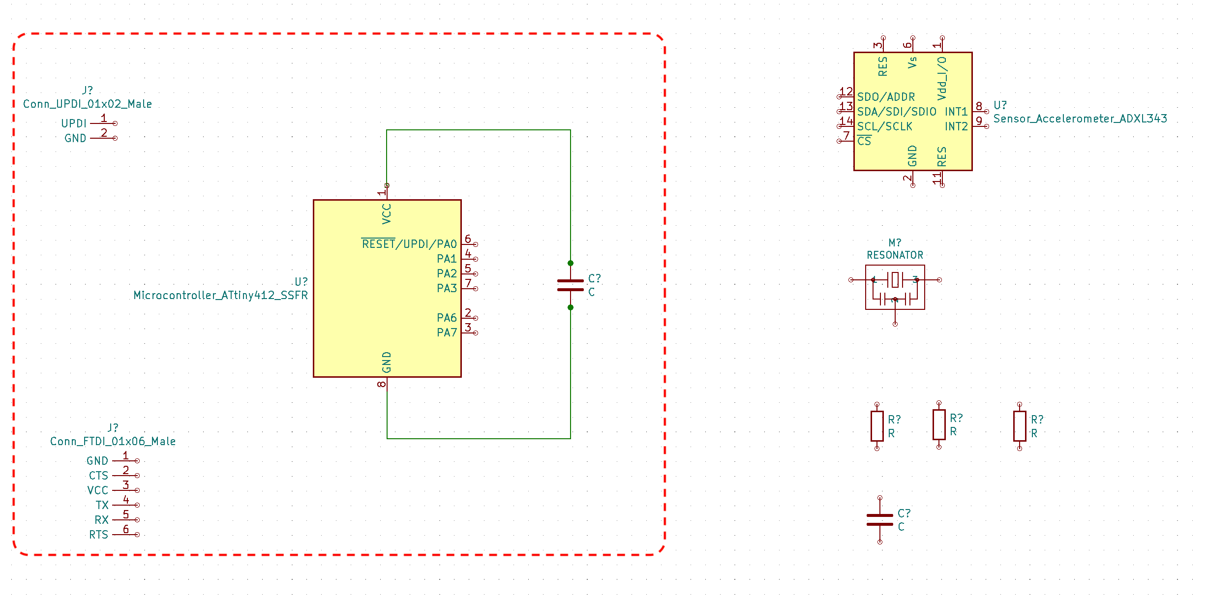
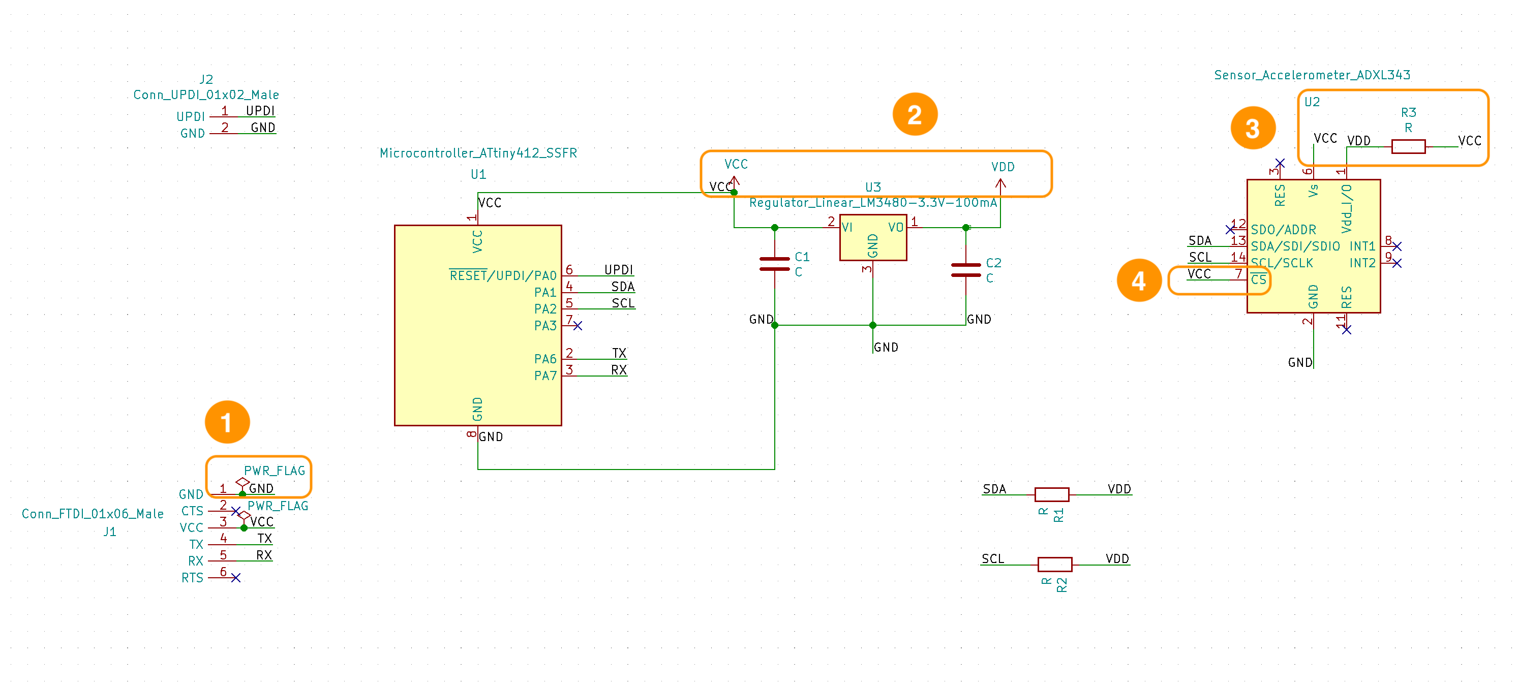
This is how the schematic for my ATtiny412_ADXL343 board looked before the annotation:
This is how my schematic looked after annotation (click Annotate schematic symbols):
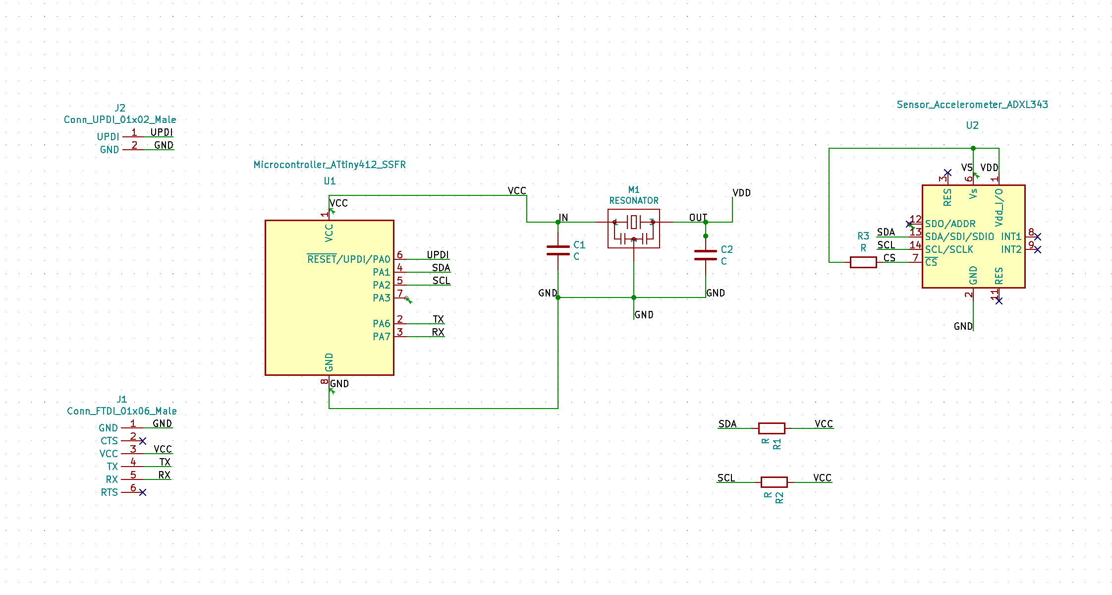
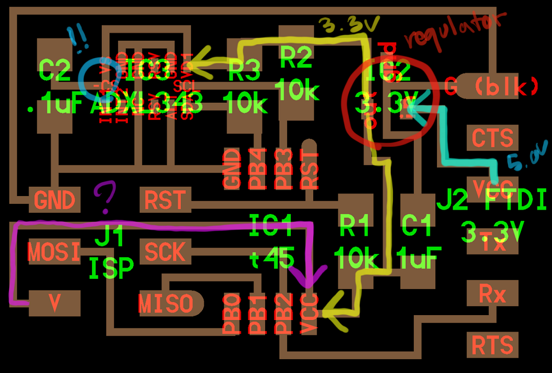
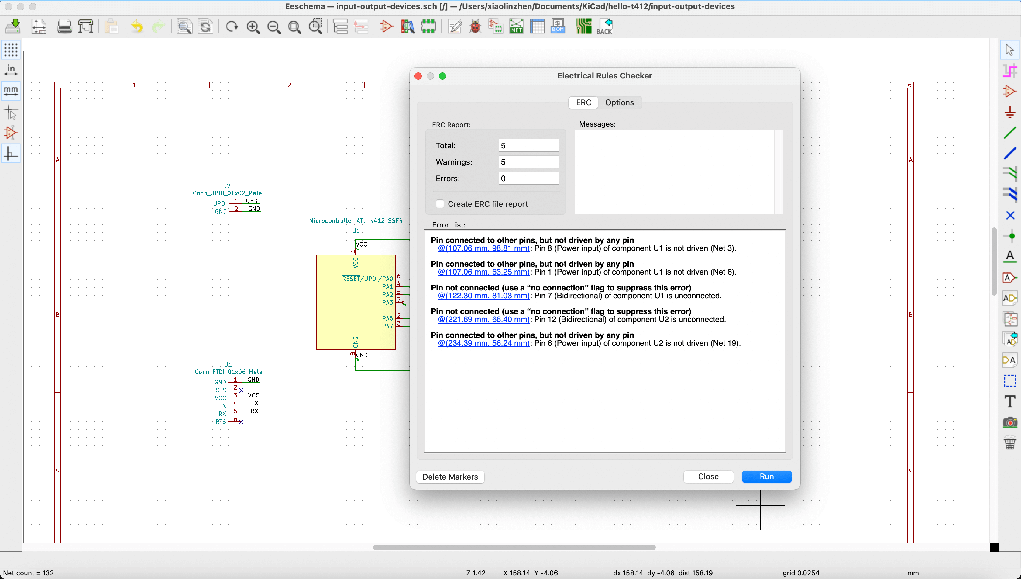
When I ran the electrical rules check, I received the error of "Pin connected to other pins, but not driven by any pin". This was becasue I had not placed the "power flag" (type "pwr" in search) on the GND and VCC of the FTDI. I also realized that I had not cross out the PA3 on the ATtiny412, and had labeled pin7 of the accelerometer ADXL343 (VS) incorrectly from the list of errors.
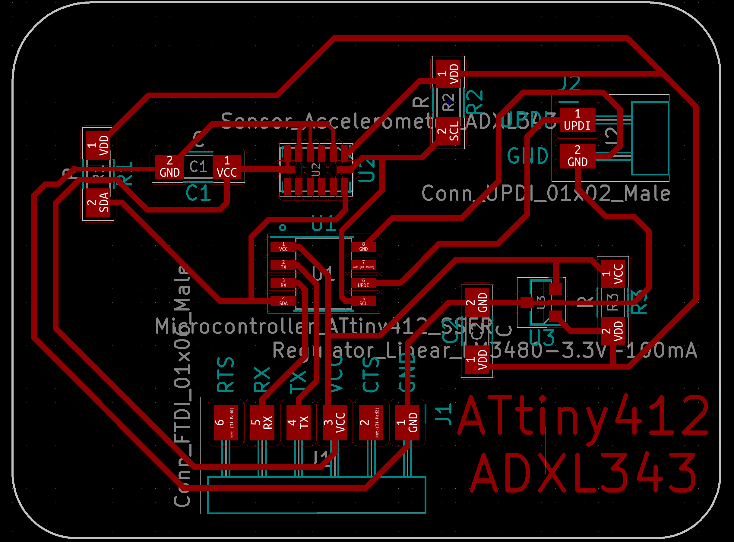
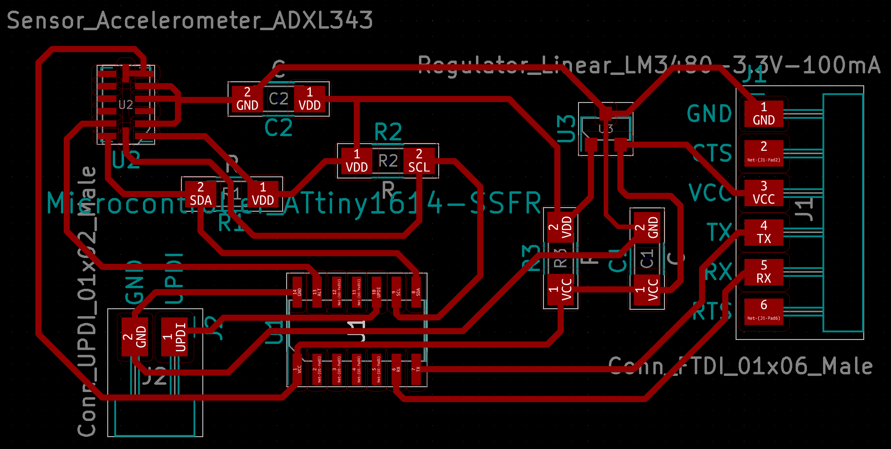
I examined the error for the VS pin, and saw the same error of "Pin connected to other pins, but not driven by any pin", and I knew that it was telling me I should either connect the pin to VCC or GND. I then looked at Neil's ADXL343 board, and learned that I should connect it to GND via the VDD pin, so I changed the label. After fixing my mistakes, I performed the electrical rules check again, this time there was no error and I was ready for the PCB layout step. Here is the final shcematic of my board:
I followed the steps that I did during the Electronics Design week to assign footprints and generate netlist. Next I loaded the netlist file (.net) to realize the PCB layout. Here is how it looked before decluterring and routing:
Part 2: PCB Schematic Issues and Troubleshooting
Apr 8, 2021Issue #1: Upon routing my board, I realized that I had placed a wrong symbol for the regulator in my schematic step. I was able to find out my mistake thanks to the 3D viewer in KiCad! The one that I used in the previous images was a resonator ("fab res"), and the correct one should be a 3.3V regulator ("fab reg"). I went back to the schematic and fixed the mistake. I then ran the electrical rules check and saw this error:
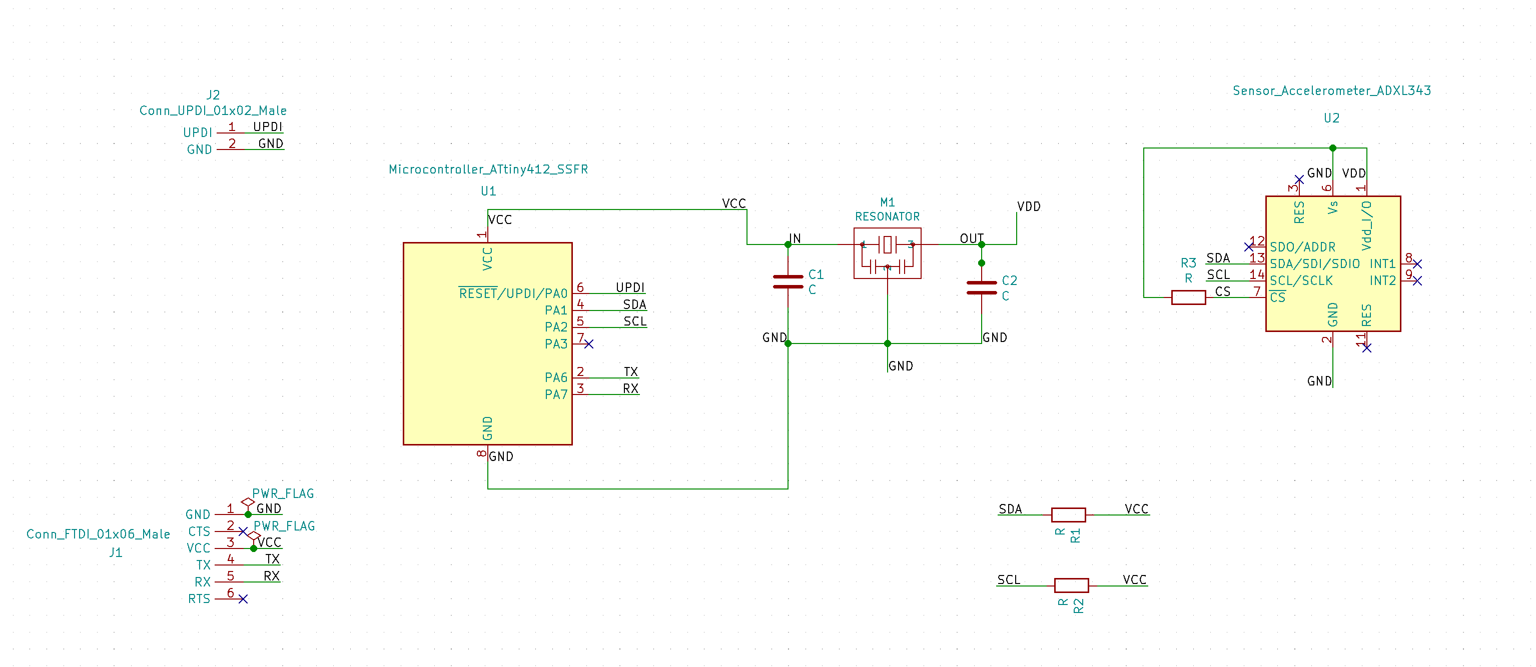
I then removed the power flag from the the GND pin of the FTDI and performed the electrical rules check, this time, there was no error. Here is how the FTDI looked:
Here is the updated schematic and unwired footprint for my board:
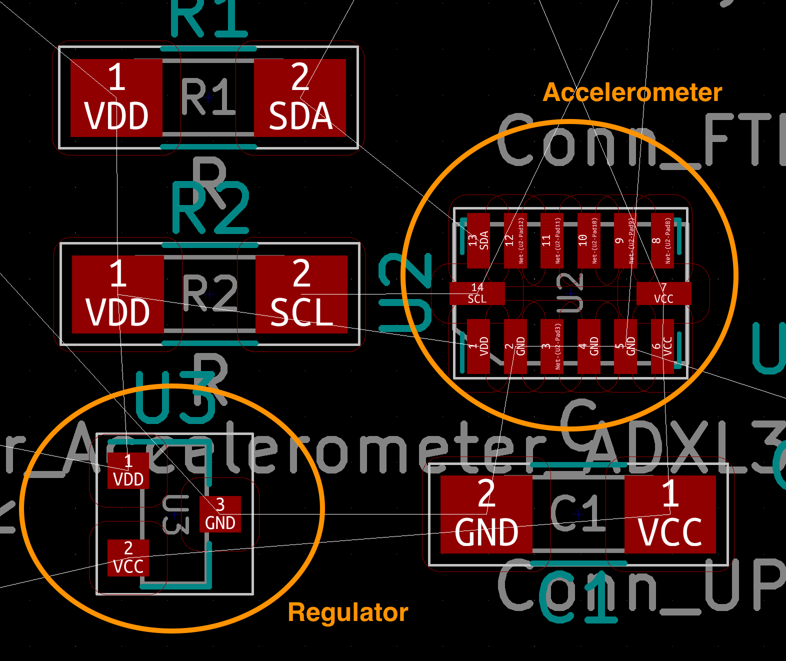
Issue #2: Then, I noticed another problem in my PCB layout: there were quite a few "GND" pins on my components! Once again, I referred to Neil's board, and I saw that in his board, the VDD, VCC, and VS were labeled as they should, so I knew that I must have made another mistake in my schematic step.
The mistake was actually coming from the routing for the VS, CS, and VDD pins on my schematic for the accelerometer. As shown in the image above, these pins all ended up with routing to the GND, and that was incorrect. I was fortunate to find Sophia's documentation on the routing on these components and fixed my mistake, here is the updated schematic for my board, highlighting the changes that I have made.
Part 3: Creating the PCB Layout
Apr 9, 2021I moved and rotated the components so that the white "rats nest" (air wires) were not tangling to each other. I also followed the steps I took in the Electronics Design week to set the clearance and track width as 0.4mm. However, I encountered my first challenge when routing the board with this track widith on the two small components: the ADXL343 accelerometer, and the GND pin for the 3.3V regulator.
The default design rule (0.4 mm) didn't allow me to place a wire on them. To work around this, I added a smaller track width in the design rule and used that on these pins. The largest width that I could use was 0.3 mm, and this was how it looked (for now) with two different track widths on these two components:
Another challenge that I encountered from the small component was that, I was not able to use the add filled zones tool to route the GND pins all at once like I did for the hello.t412.echo board, so I must routed my GND pins manually. In the end, I was able to connect all the components and this is how it looked:
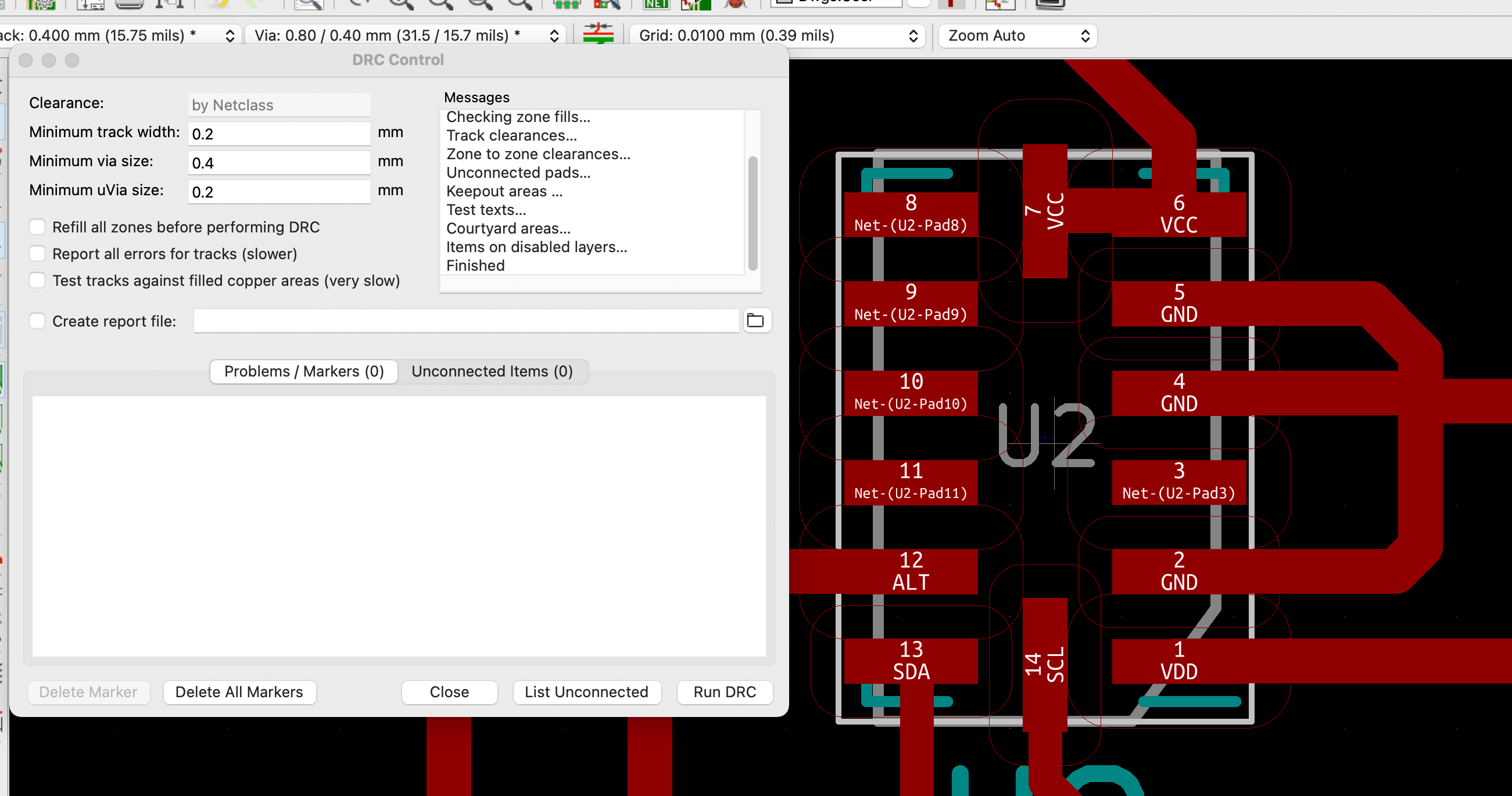
I then ran the electrical rules check in the PCB layout, and received an error of "Pad too close to pad for the accelerometer.
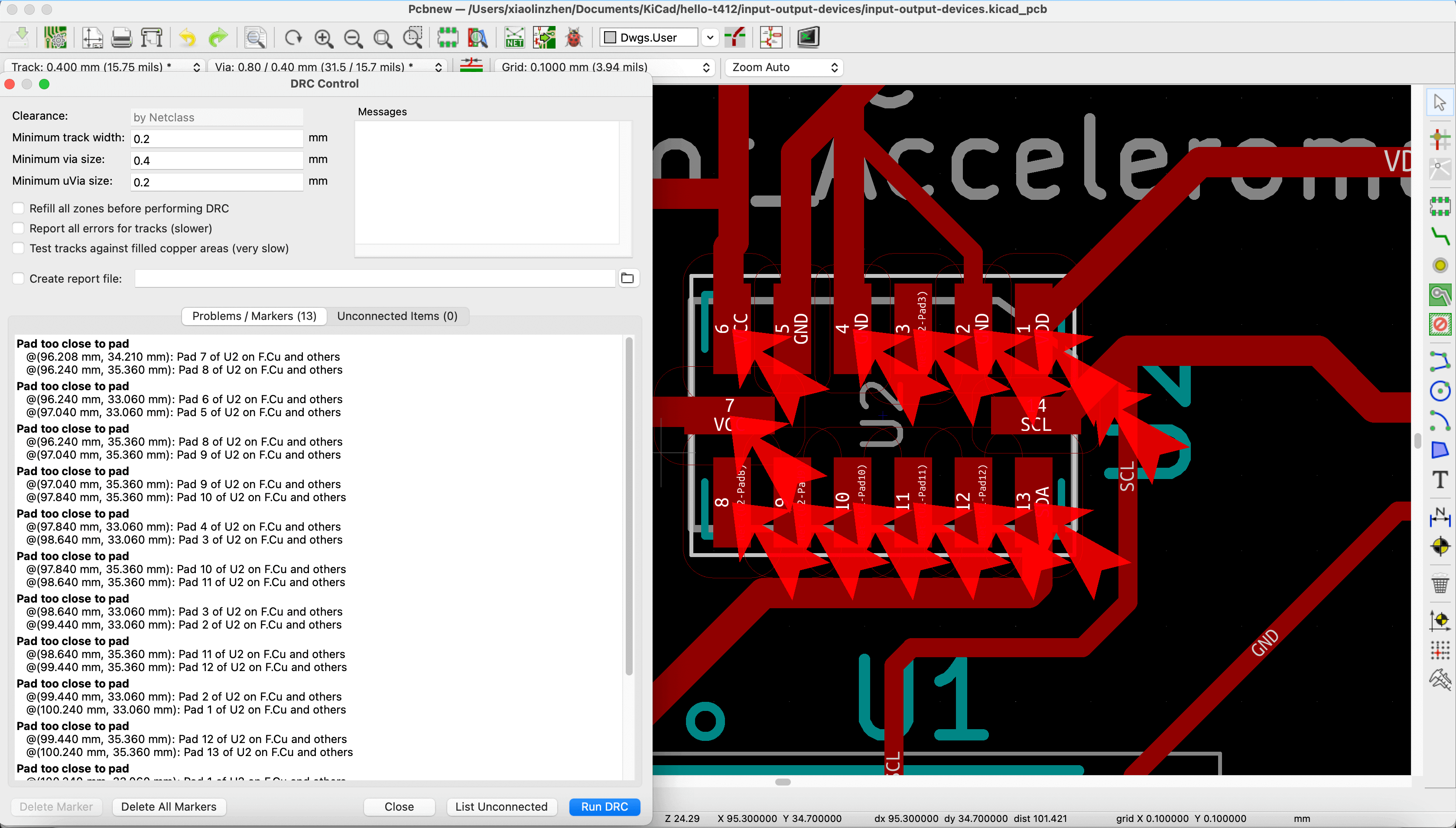
Once again, Rico's documentation helped. In his documentation, he addressed that we could modify the footprint of the component. He had used EAGLE for PCB design, so I then looked up online for the solution in KiCad on this, and this was the tutorial that I found helpful for editing the footprint in PCB without altering the library from which it came.
The component for the ADXL343 accelerometer in KiCad was the LGA-14_3x5mm under the fab library.
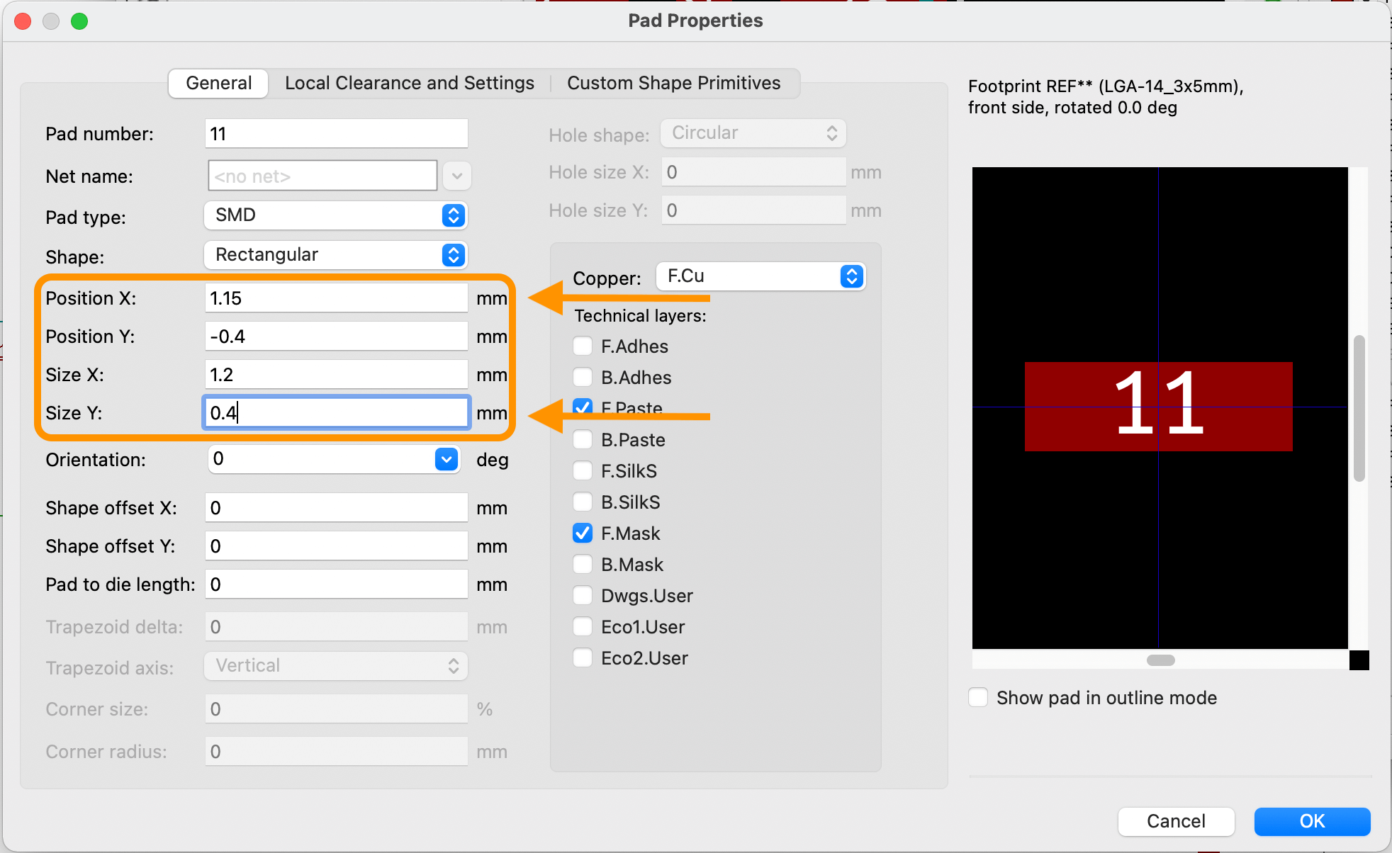
To modify the footprint for the accelerometer, I used the Edit a footprint tool in KiCad and adjust the sizes of each padto allow for 0.4mm clearance between each pad of the component. For each pad, I reduced its width from 0.5 mm to 0.4 mm ("Size Y" for horizontal pads, or "Size X" for the two vertical pads), I have also set "Position X" 0.05 mm further away from its original setting (i.e. changed 1.15mm to 1.2 mm).
As a side note, I still had to use 0.3mm for the track width running from the GND pin of the regulator.
Once that was done, I ran the electrical rule checker. This time, there was no error.
Part 4: Fixing Mistakes and Upgrading the board with ATtiny1614
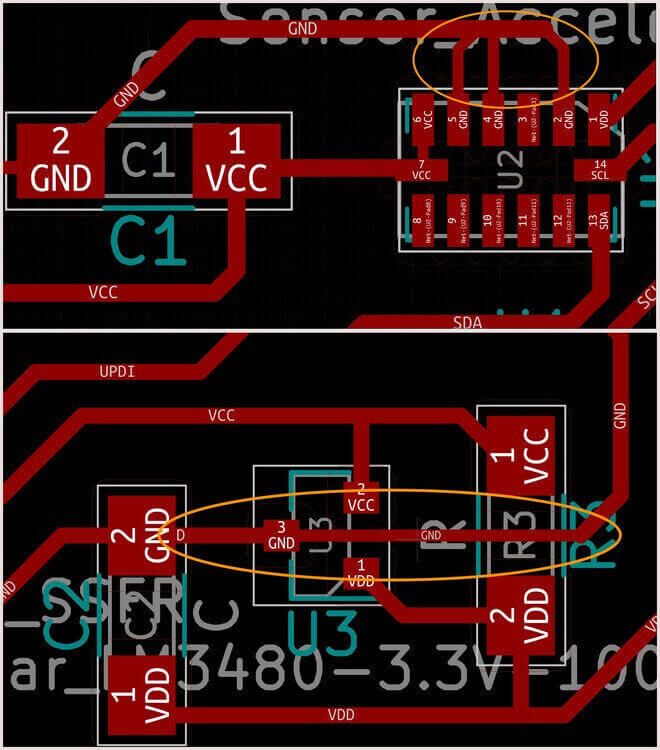
Apr 10, 2021While double checking my final ATtiny412_ADXL343 board, I noticed that I had made a major mistake: I had connect the voltage resource directly to the accelerometer, instead of bypassing the 3.3V regulator. As shown in the image below, the last stop for the VCC was the regulator in my case, and this was a very critcal mistake because the role of the regulator was to output a clean 3.3V needed by the accelerometer, and I would burn my ADXL343 right away if I were to use the board.
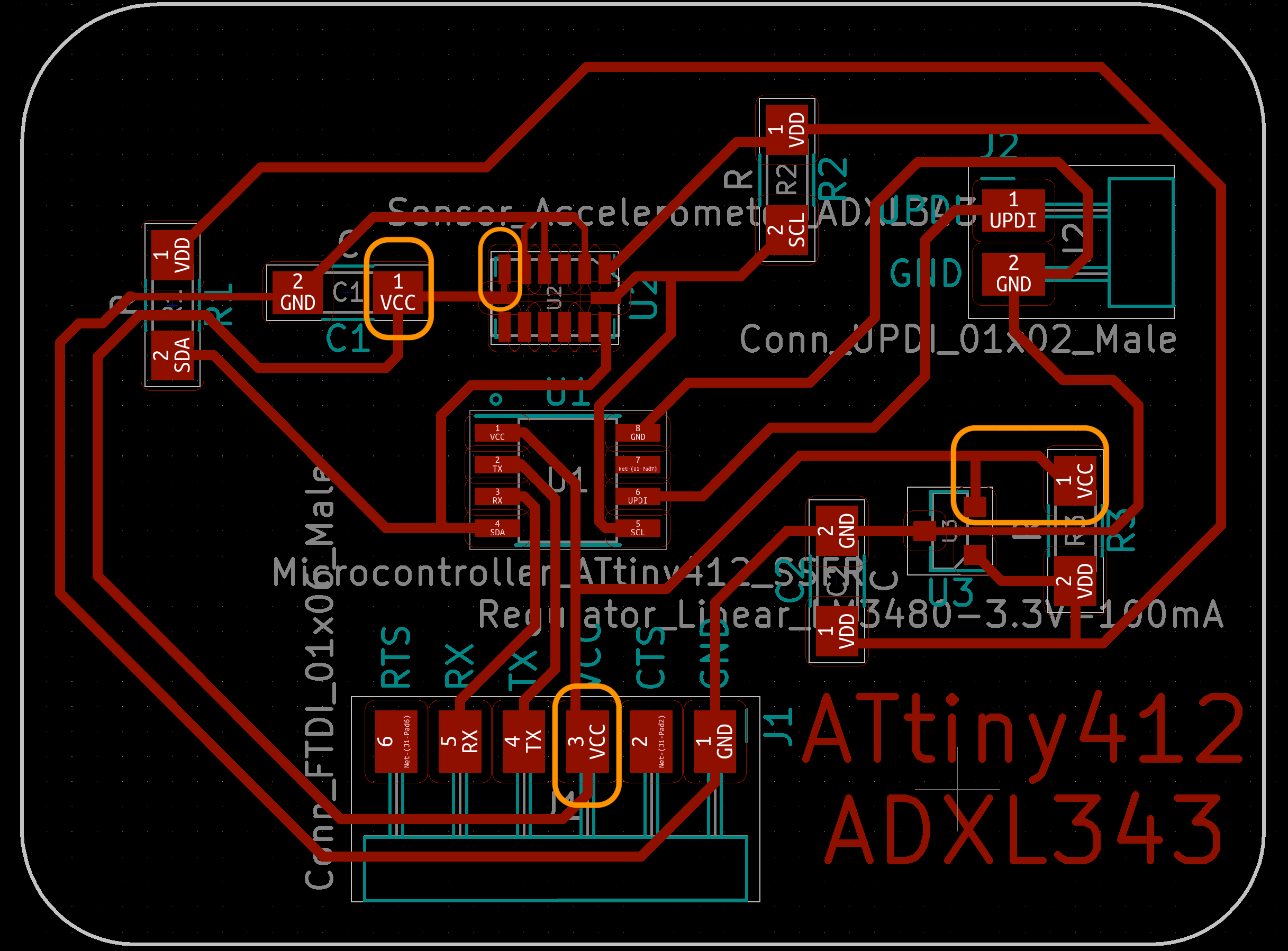
After examining Neil's board more carefully, I noticed that there was something different between my board and his board:
- Neil had chosen to use the SDO/ALT pin in ADXL343 and I had put on a "no connect" for the pin: After reading the ADXL343 datasheet more carefully, I learned that I could use the pin as an alternative I2C pin.
- The NC pin was missing in the ADXL343 symbol in KiCad -- According to the datasheet, the NC pin was not internally connected, and since the fab component for the ADXL343 was the same as the one from the manufacturer in KiCad, however I am not sure if this would be a big issue or not in the programming later on.
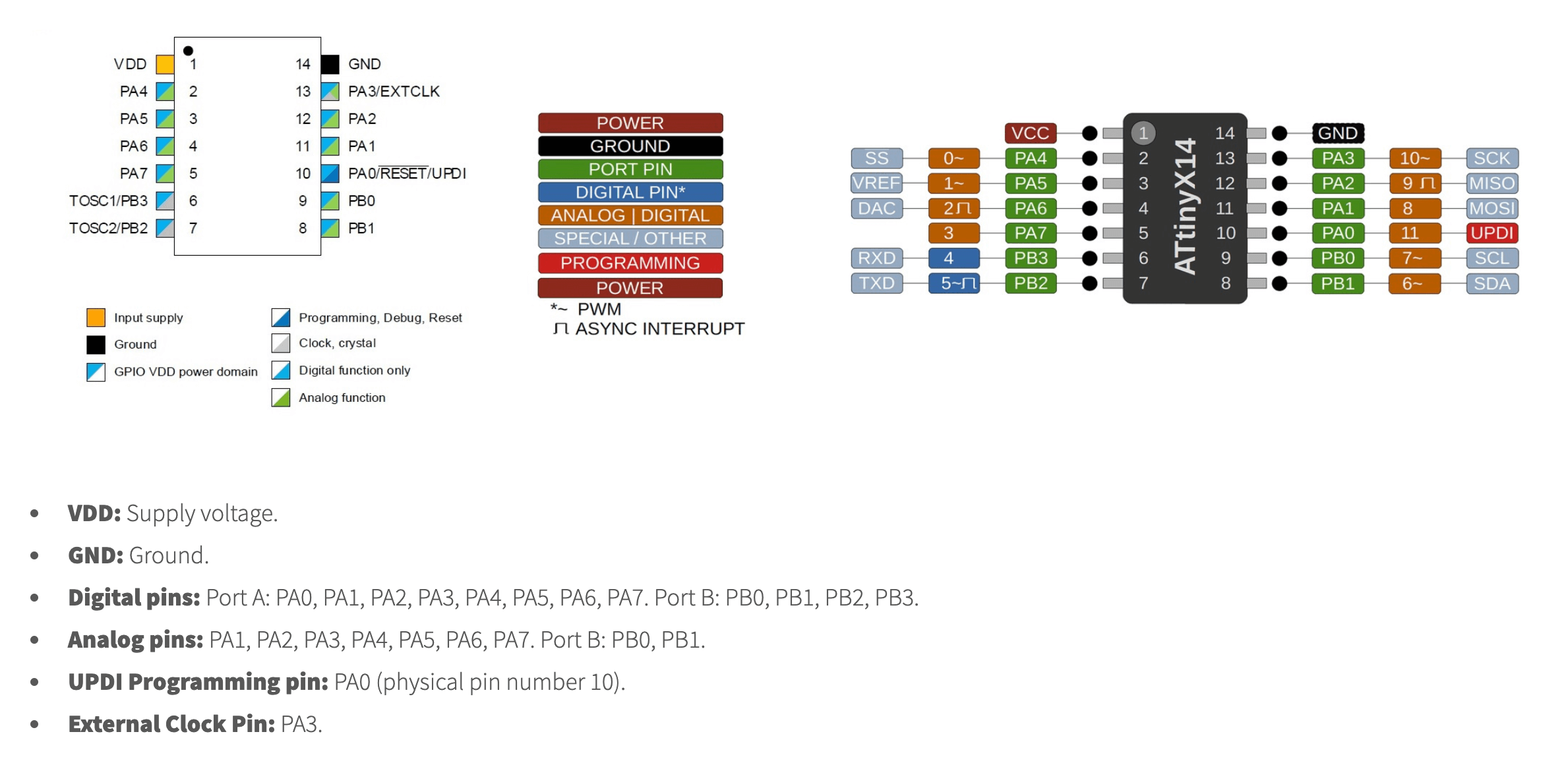
I decided to add the ALT pin for the acceleromter but then I realized that I could also use the opporutnity to upgrade the microcontroller since I had used up the pins for the ATtiny412. In the end, I chose to use the ATtiny1614 as my microcontroller. I used Spence Konde's pinout summary as my reference to locate the correct pins when updating my schematic. I have set to use the following pins on the ATtiny1614 for this assignment:
- VDD, GND and UPDI pinswere default
- TX pin: PB2 (default pin for TX)
- RX pin: PB3 (default pin for RX)
- SDA pin: PB1 (default pin for SDA)
- SCL pin: PB0 (default pin for SCL)
- Alternative Pin for I2C: PA3
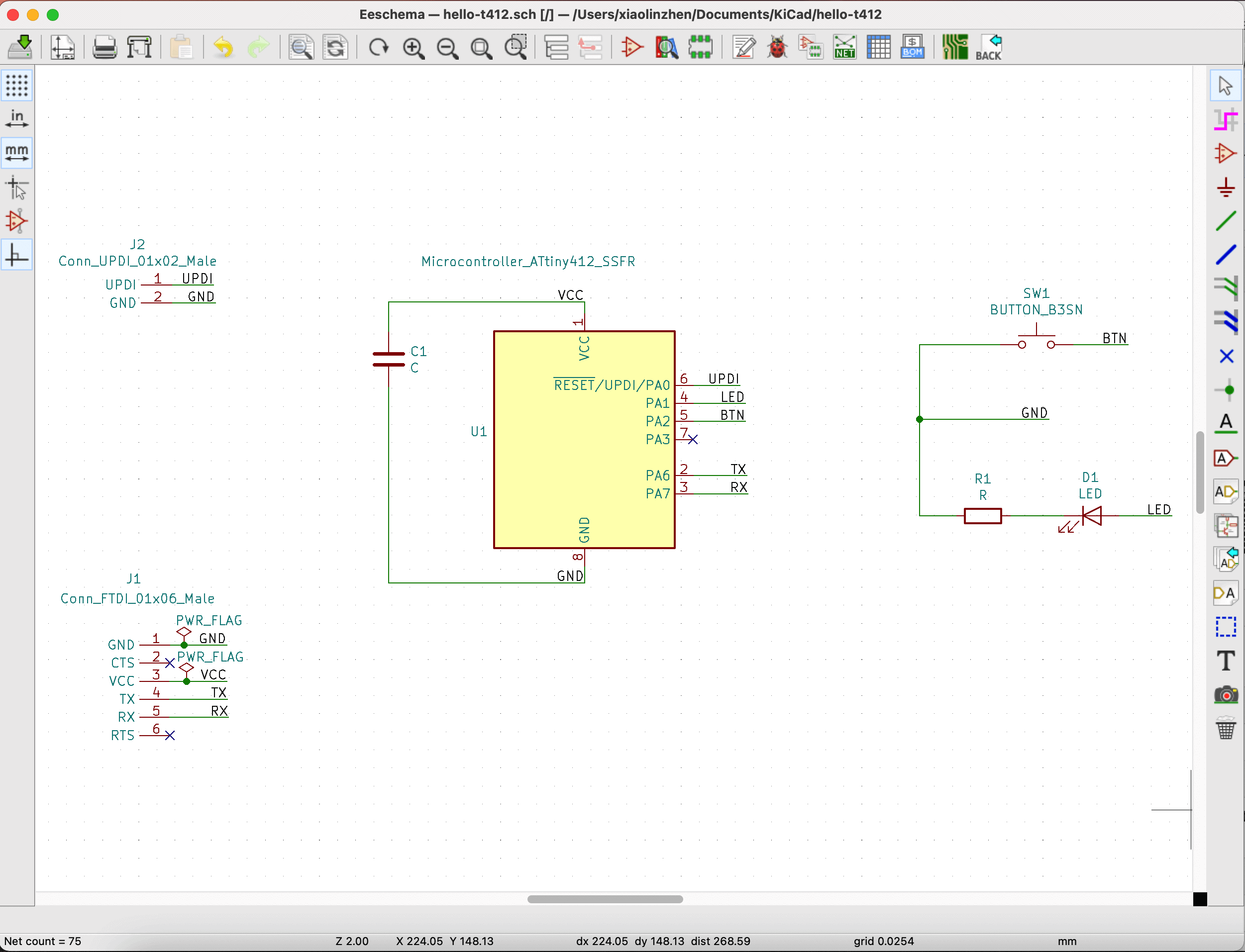
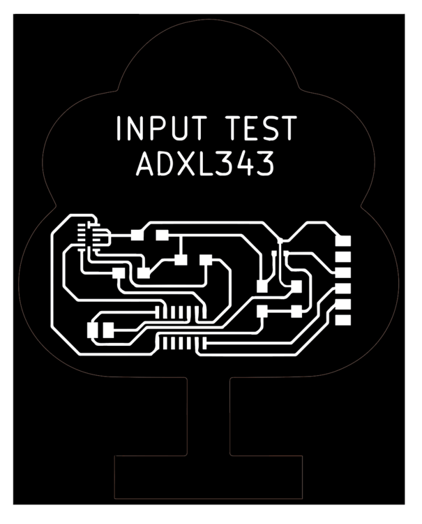
Here is the schematic for my ATtiny1614_ADXL343 board:
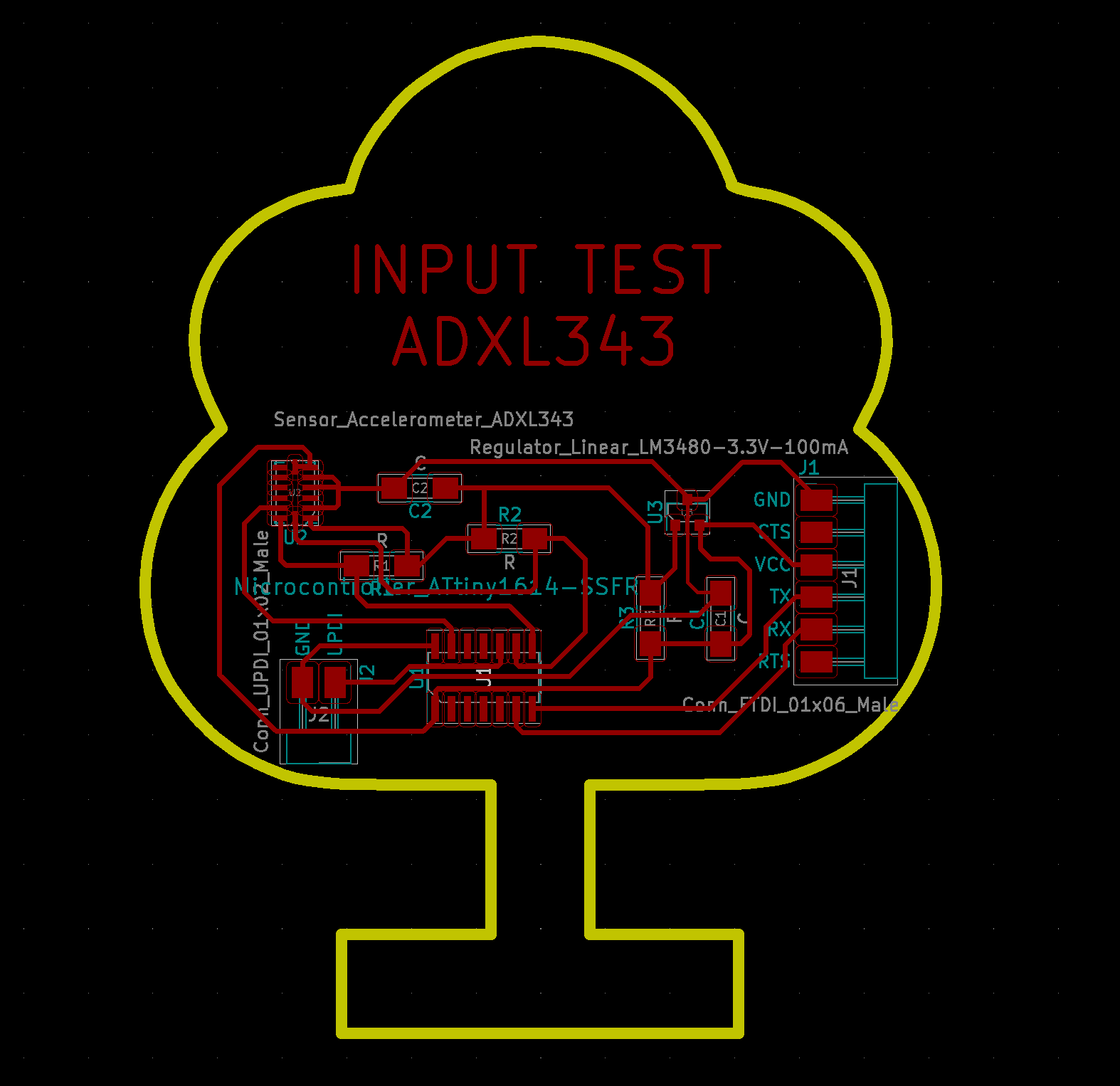
Here is the PCB layout for my ATtiny1614_ADXL343 board:
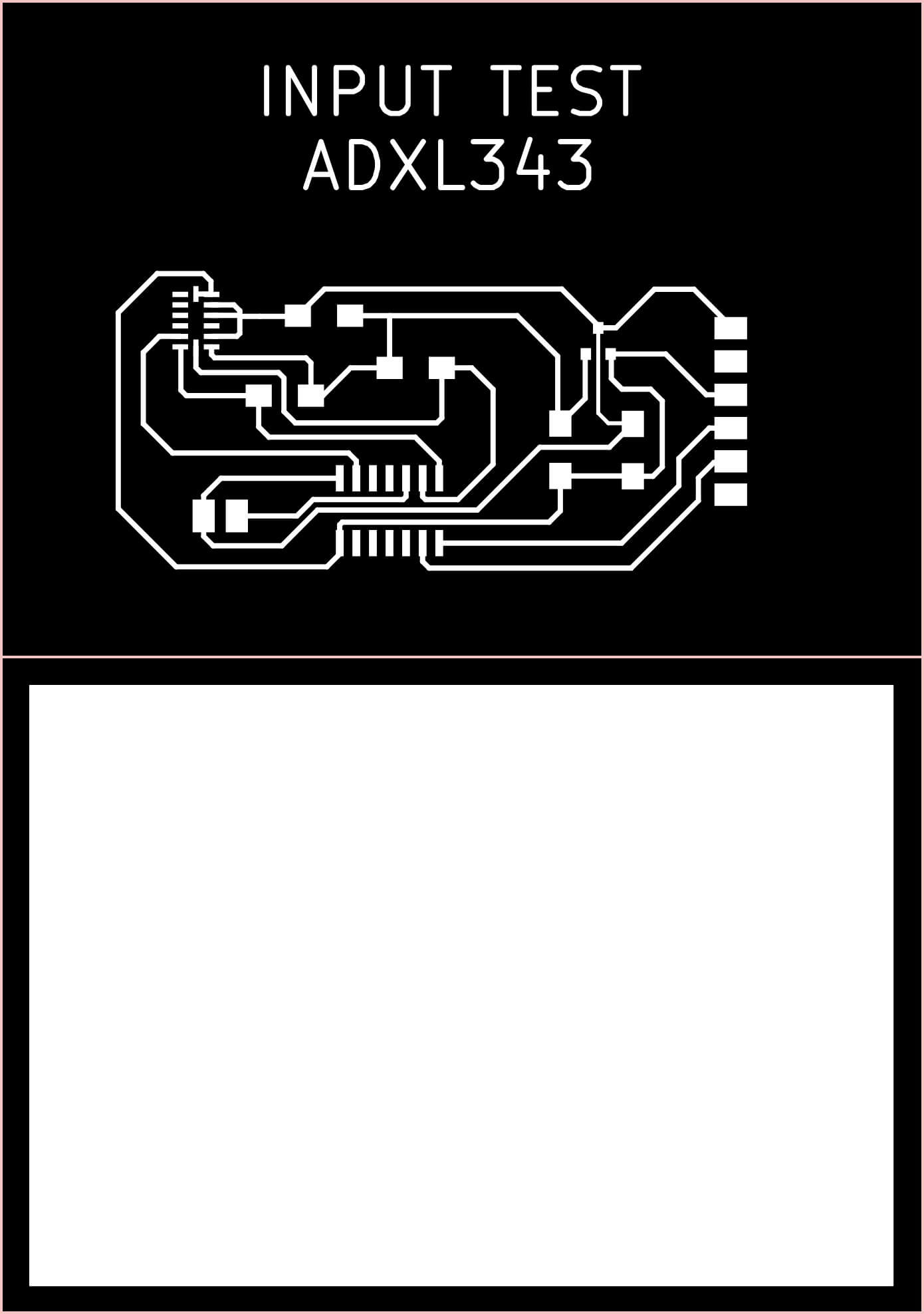
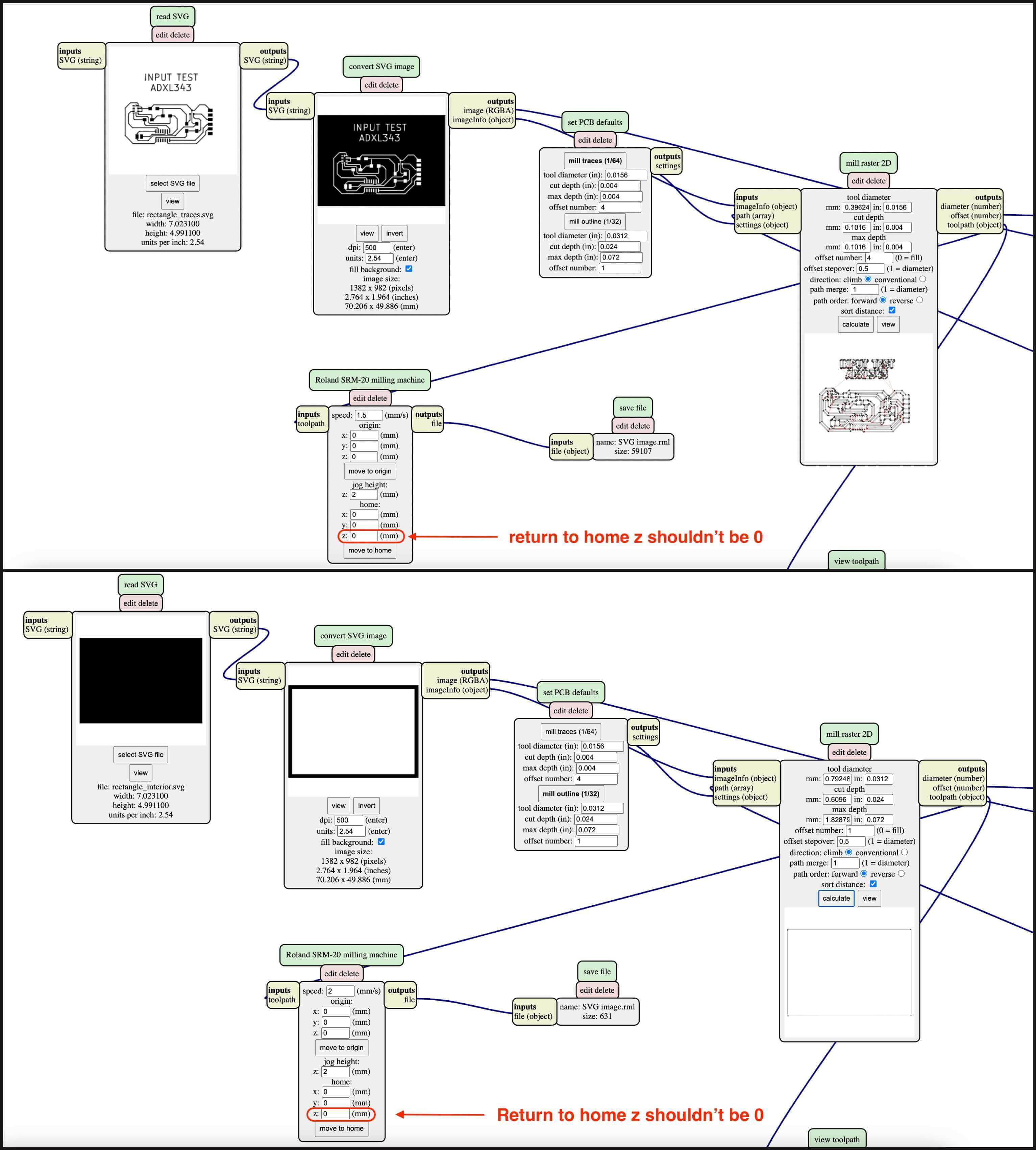
I then exported the traces and the interior, and post-processed in mods for milling. Here is how the traces and interior looked after inverting the colors for correct milling:
Apr 11, 2021
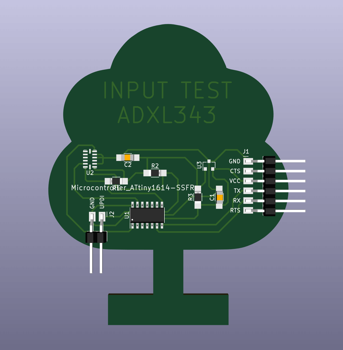
I also experimented with importing (File > Import > Vector Graphics File) a DXF file of a tree image for the board outline, and set it as the Edge Cut. Here is how the tree board looked in 2D and 3D view:
When importing the dxf file, I also set the line thickness as 20mm because I wanted to create a border for the outline, but this proved to be an issue for the fiber laser process later. I should have just imported it as 0.001" stroke thickness since that would be the cut line.
PCB Making
Apr 12, 2021Using PCB Milling Machine
I used mods (cba edition) generate the G-code files (.rml files) for the Roland SRM-20 PCB milling. The process of board fabrication was similar to Week 4 Electronics Production, so less details will be contained in this week's documentation. For this exercise, I used the Program > Open Server Program > SRM-20 > PCB svg program since the files exported from KiCad was in .svg format instead of .png. I also decided to use the default setting for the traces (i.e. offset = 4) to to allow for enough copper traces left for the ADXL343 accelerometer.
I learned this week that I have been making the same mistake for the z height in the return to home setting (and finally knew where to fix it!). I have been setting the origin and home position as (0, 0, 0) and experienced a scratch on my boards. I consulted my instructor Spencer and he told me that most likely this was due to the return to home z-height set as 0 instead of some positive values. Here are the settings I used to generate the G-code files for the traces and interior of my board:
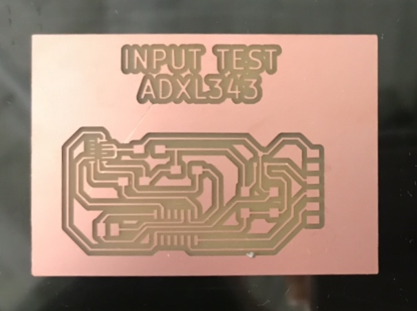
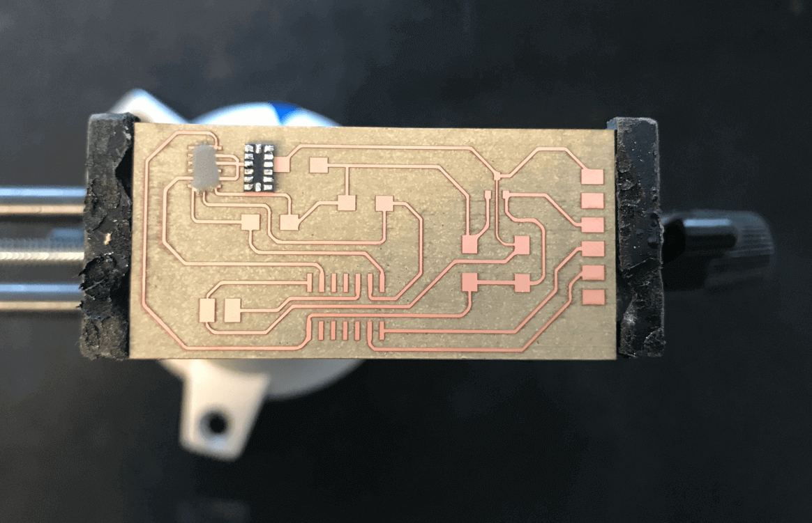
Here is how my board looked, thankfully the scrach was not deep and didn't cut through my traces, so the connections were still there. I was also relieved to see how well the traces for the accelerometer were fabricated.
Using Fiber/CO2 Laser Cutting Machine
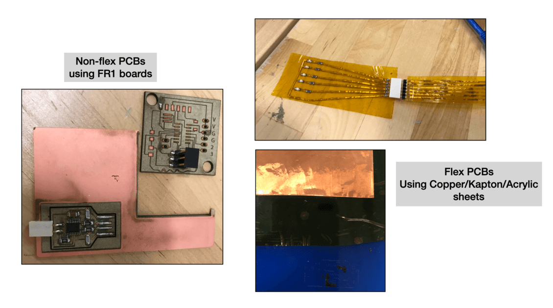
On Monday, we receieved an thorough training from our Instructor, Spencer on the fiber laser cutting machine! I have been looking forward to learning this skill becasue his process has shown promising results in flex PCB production, which is something that I am looking to do for my final project. A detailed fiber laser tutorial can be found on Spencer's webpage.
From the training, I learned how to use the fiber laser lens (a fiber/CO2 combo lens) to produce non-felxible PCBs on FR1 boards, as well as flexible PCBs on Copper/Kapton/acrylic sandwich sheets. Compared to the FR1 PCB production, the flex PCB required more design consideration (i.e. solder mask) and weeding in between processes.
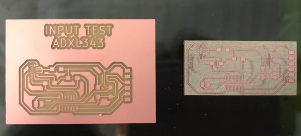
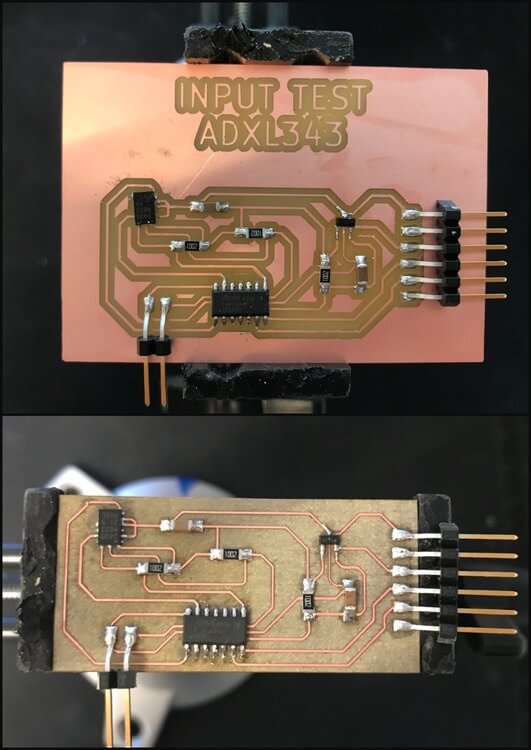
After the training, I seized the opportunity to laser cut my PCB using an FR1 board. Here is a side-by-side copmarison for the milled board and the fiber laser cut board, in my opinion, this was the most beautiful board I have made so far:
Let's see what I have learned from this experience!
- As I planned to laser cut my tree board, I exported the trace and interior files in .svg format from KiCard and used mods to convert them to .png format. In this step, I needed to invert the colors for the traces file but I didn't need to invert the color for the interior as it was exported as Edge Cut from KiCad, meaning that the colors were correct for PCB production. I used the default dpi value 500 in mods to generate the png files. Here is how the files looked after post-processing from mods.
- Spencer shared a nice way to import the png files without opening them in a new window: 1) Create New > Custom; 2) File > Place. However, we noticed that there was a scaling issue for the .png files. I then experimented with importing the .svg files the same way and didn't have the scaling issue, so we concluded that could be a bug in the conversion process in mods.
- Next I clicked File > Print to connect to the JobControl software for the laser cutting machine. In this step, I made sure to select the top left corner for placement (default: center) and set the resolution as 1000dpi (default: 500dpi).
- The following machine settings are specifically for the fiber laser cutter. Most of the steps have been performed by Spencer during the training so I only double checked when cutting my board:
- JobControl:
- Lens: 2.85 in (flexx) (**default: 2in)
- Material Folder: Dassault-2020-Testing\fabAcademy
- Material: FR1 PCB
- Laser cutting machine:
- Uninstall the CO2 (only) lens: bottom spacer > top spacer > middle lens
- Install the Flexx lens: bottom spacer > top lens (**make sure to change this back after use)
- Zero the PCB using the brass knob focusing gauge: Similar to the traditional laser cutting process, we need to perform this step every time we change the position of the PCB / change a new file.
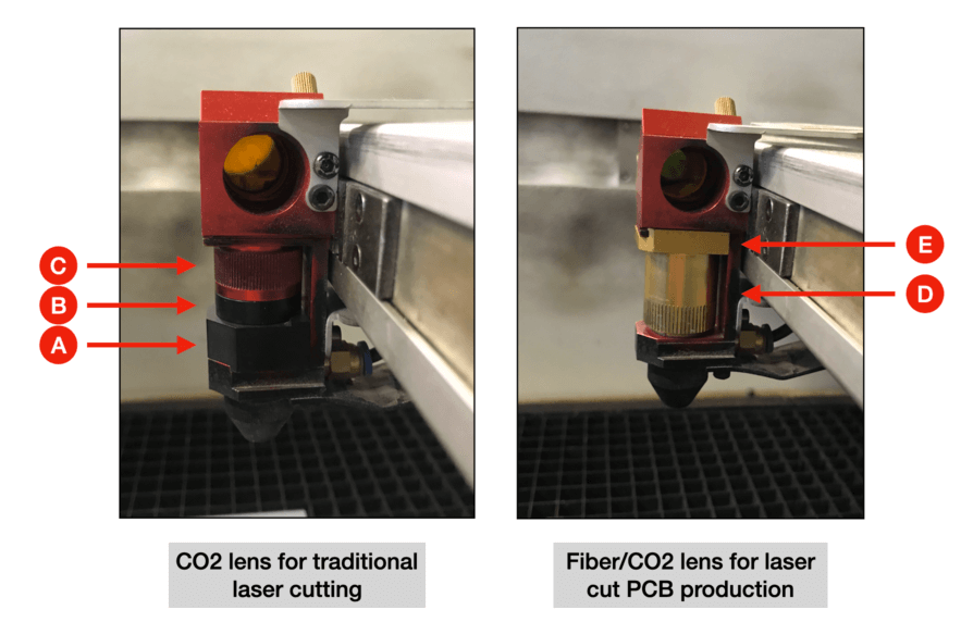
CO2 lens vs. flexx (Fiber/CO2) lens
- JobControl:
- Then I updated the job in JobControl but the estimated time as 74 minutes for engraving the traces (fiber laser) and 0 minute for cutting the outline (CO2 laser)! Spencer also found this strange and we tried a few more times but didn't have success. In the end, we trimmed down the file to have the traces only, and framed it with a red rectangle as the cut line. Here is the final file for laser cut. The estimated time for the raster process (engraving / fiber laser cutting the traces) was 21 minutes and the vector process (CO2 cutting the outline) was 22 seconds!
- Here is a short video of the laser cutting process:
- Towards the end of the process, we found that the top left part of the board were not processed completely, this was mainly due to the board not being flat. So I re-zeroed the PCB towards the center of the board, and ran the job again, here is a short video of the process:
- When the job was complete, I took out the board and found that it was not cut through, this could be because the FR1 board that I was using was double-sided board so it was a thicker board (~ 0.4mm thicker). In a traditional laser cutting process, we could just raised the power to cut the whole board through, but we shouldn't do it here since we are not supposed to cut the copper layer with a CO2 lens. Using a box cutter, I was able to remove the PCB from the FR1 board. I then post-processed the board with soap and water and was ready for soldering!
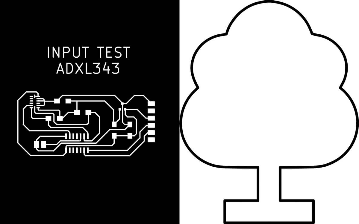
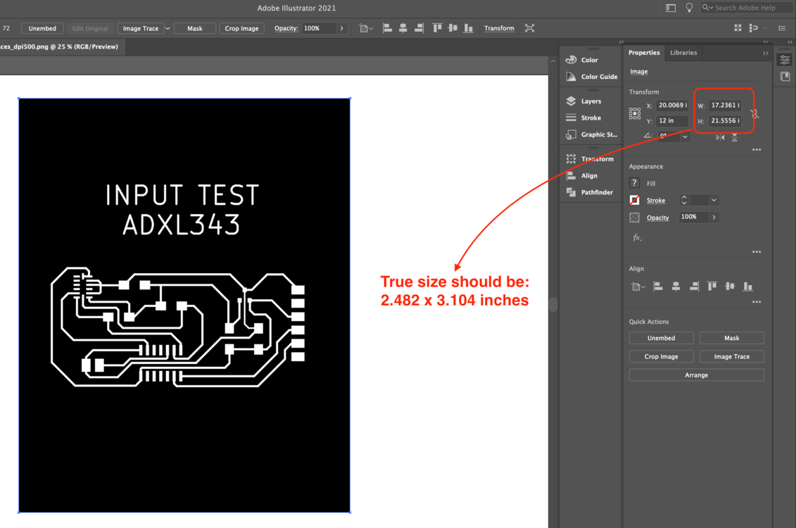
I continued with the .png files as I only had the colors inverted for them. I then adjusted the width and height to be the true size of the board, and vector traced and expanded the images (Object > Image Trace > Make and Expand). The interior was going to be the cut line, so I set the color as red with 0.001" stroke thickness. However, due to the line thickness mistake I made in KiCad, there were two vector profiles generated for the tree outline.
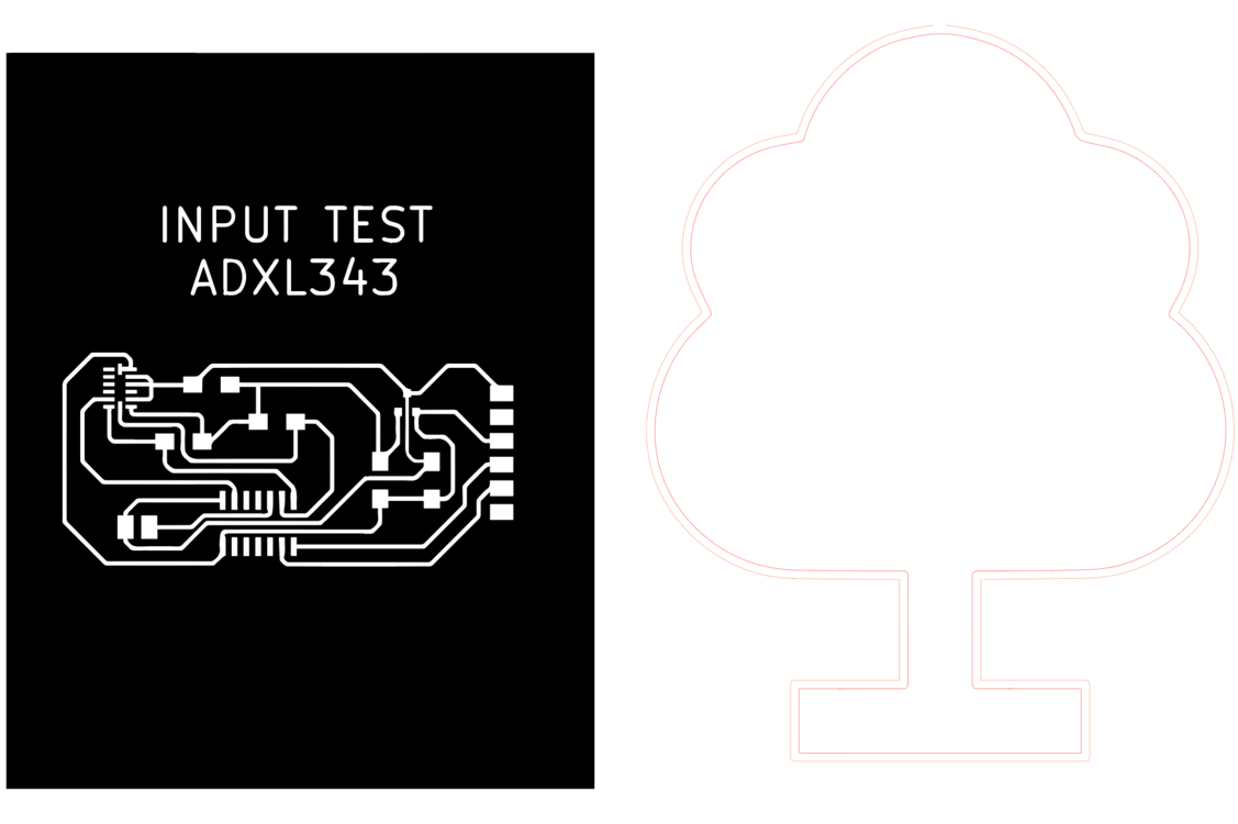
To recetify the issue, we only used the "inner tree profile" as the cut line. I supermiposed the interior with the traces, and brought the traces file to the front (Right click > Arrange > Bring to Front). This is how the fiber laser file looked:
Spencer told us that the computer remember the settings from last time so we must make sure to change back to default setting once we finish using the fiber laser.
Soldering
I was told by my instructors that the ADXL343 accelerometer was a challenging component to solder with, so I had prepared 3 sets of components to get myself used to the soldering process.
During the Global Lecture, Neil showed us how to do a reflow soldering for this component. Doing more online research, I then acquired this solder paste over the weekend as it could help with the reflow soldering. On Monday, after the fiber laser training, my classmate Griffin showed me how to do reflow soldering with solder paste and hot air gun. I needed to be careful and not to plunge out too much paste especially because I didn't have a finer dispensing tip. I started with the ADXL343 accelerometer, I tinned the pads under the component, and covered the copper traces with a tiny bit solder paste.
I used the hot air gun to melt the paste to allow it to spread out the paste over the traces, then carefully lined up the ADXL343 component with the copper traced. Next, I heated until the paste changed consistency and color. After that, I used the reflow soldering technique on the other components but I found that it was easier to use the traditional technique on the resistors and capacitors since their pads were a little apart from each other. Here is how the soldered boards look:
Testing the Board
The final part of the assignment was to test and program the board. In this process, I used Arduino IDE and its Serial Communication. As mentioned above, the SCL pin is the clock signal pin, and the SDA is the (serial) data signal pin. I started with a simple sketch created by Sophia and modified the SDA pin information to see if the accelerometer could be detected.
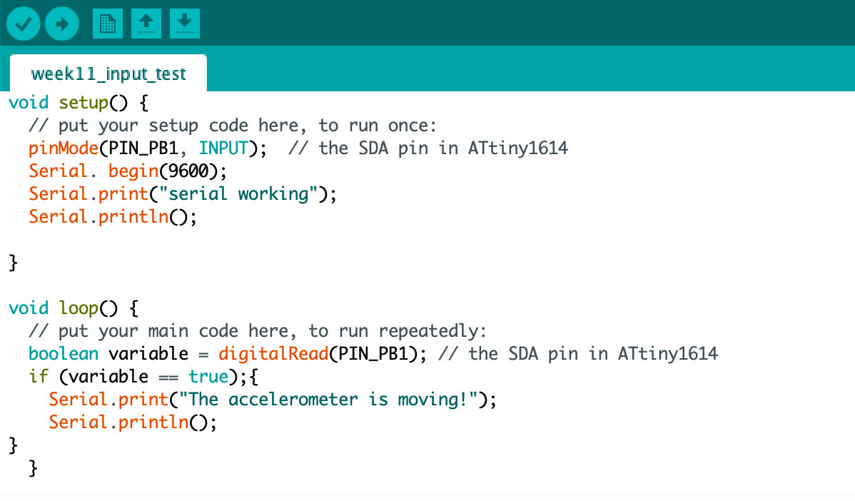
I followed a similar process I did in Week 6(Electronics Design Week) and Week 8(Embedded Programming Week) to connect the pins between the boards. Here is how it looked:
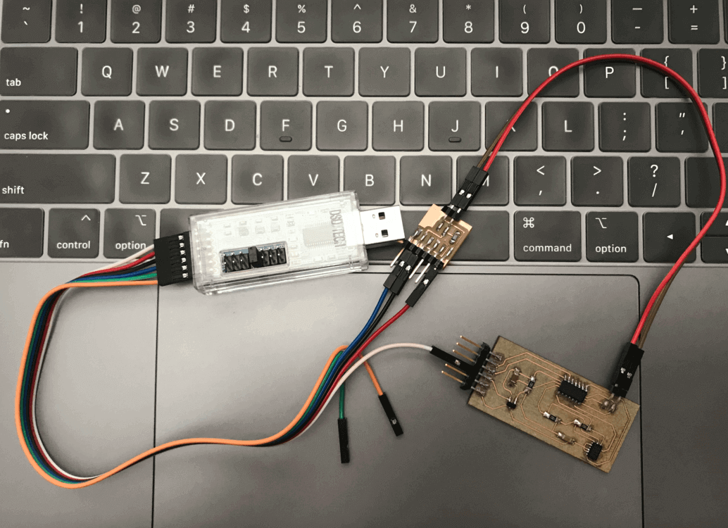
I used the 5V logic level in the FTDI USB connector (the blue USB connector) and plugged it to my computer. Then I uploaded the sketch but I received the following error: UPDI initialisation failed.
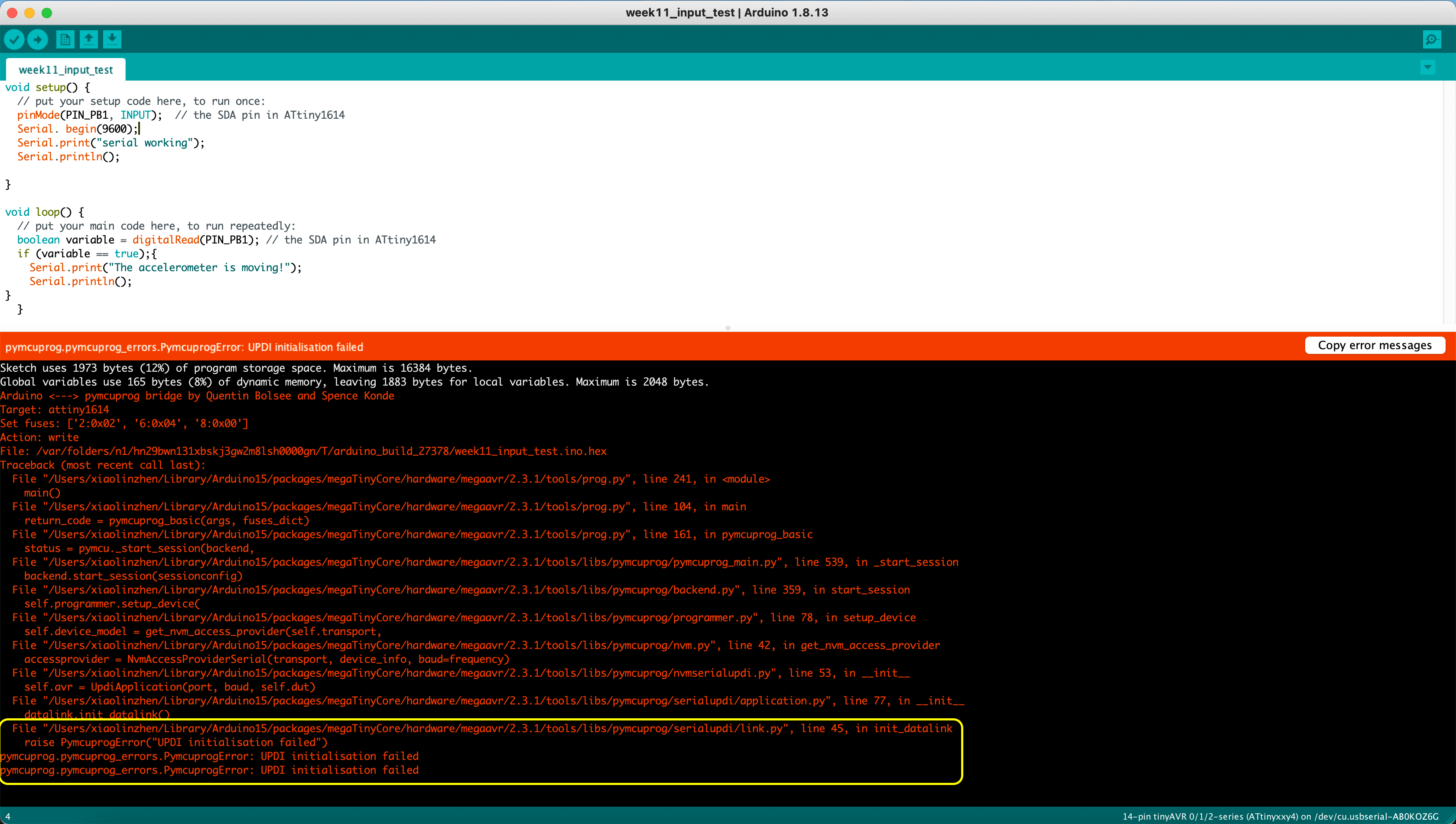
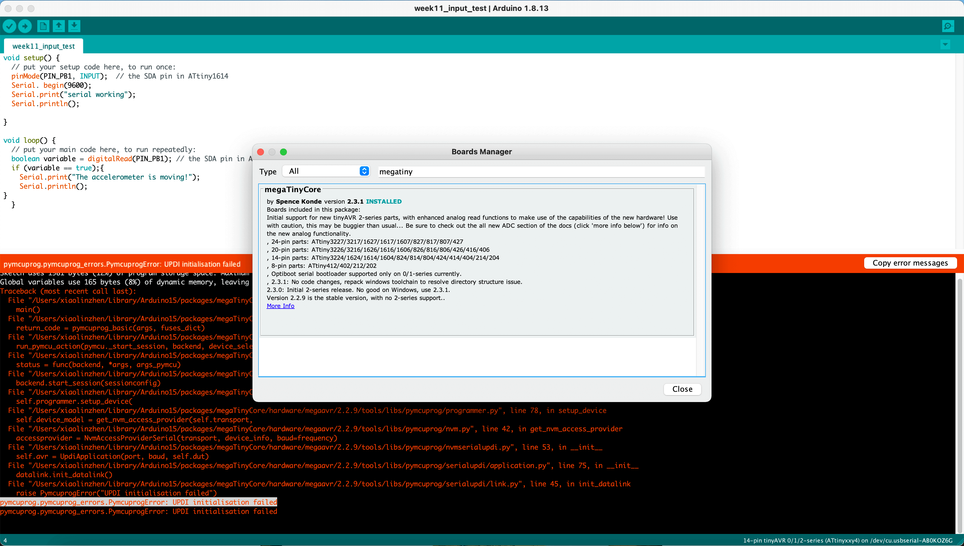
I tried a few more times, uninstalled and reinstalled Arduino IDE, updated the megaTinyCore, and switched to use the 3.3V logic level. I also made sure I have selected to correct board, port, and programmer, but I still experienced the same error when uploading this sketch.
I looked up online and found Spence Konde's response regarding the issue.
The thread was for an older version of the board (the version I am using now is 2.3.1) but I thought this could provide some hints. My eyes settled on the 4th line for the pin has a big capacitor on it and I doubted if that was the reason: I intended to use a 0.1 uF capacitor for the accelerometer, and the 1 uF capcitor for the microcontroller but I was not sure if they were too big or too small for the board...
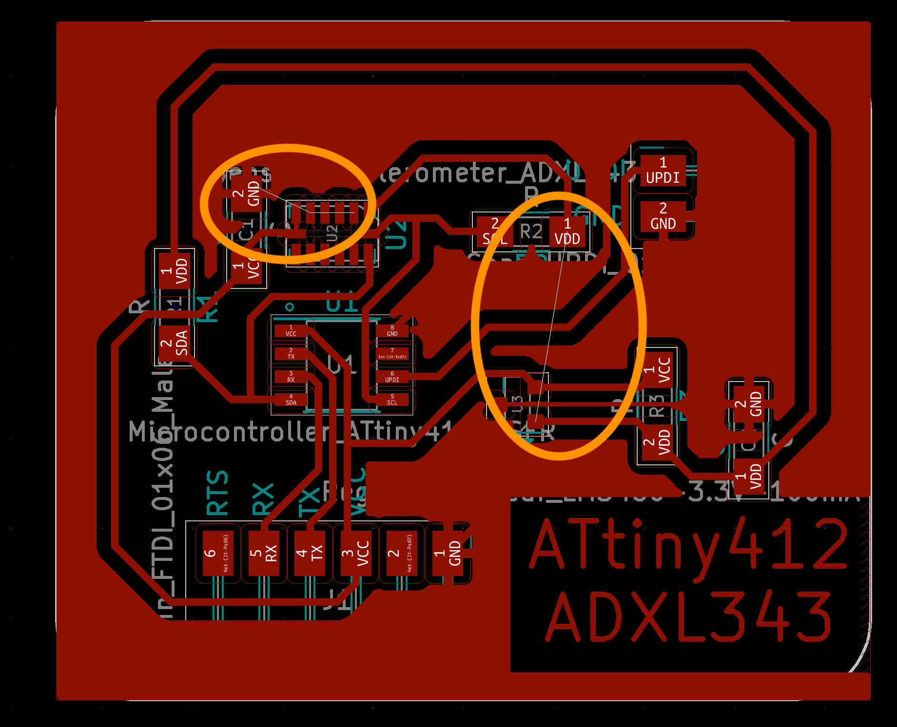
While experimenting with various possible solutions, I felt that the FTDI USB adaptor was getting quite warm, and it occasionally disconnected and was not dected by Arduino. I didn't recall until then that I should run a continuity test. I started with testing the GND pins, and I found that connected the VDD line for the SCL pull-up resistor to the GND!
Here is a short video for the continuity test on this line:
I chased down the line and found that the error started with the accelerometer: I must have bridged the VDD line accidently with one of the GND pins running the hot air gun on the board. Again, from Sophia's documentation, I learned that I could increase the sucess rate by covering the board with a (laser cut) mask to expose the pads only. Later, I learned from Kitjia's documentation that, insteading of using 0.4 mm as the clearance, I could also change it to 0.3 mm to pass the eletrical rules check for the ADXL343 accelerometer!
Debugging the Board
May 10, 2021During week 14, I upgraded my board from using ATtiny 412 to ATtiny1614 as the processer, I also upgraded from using the ADXL343 accelerometer to LSM6DS33 3D Accelerometer and Gyro module as the input device of my project.
The reason for that was because the LSM6DS33 combines a digital 3-axis accelerometer and 3-axis gyroscope into a single package. This board also uses I2C networks so I called out the SCL and SDA pins in the ATtiny1614 microcontroller.Here is the functional video featuring the board and the module. Please visit my Week 14: Networking and Communication documentation for more information.
May 22, 2021
UPDATE: During Week 14, I upgraded my processer from the tinyAVR-1 series to an ESP32-WROOM for its bluetooth feature. I was also able to put my I/O devices in one board. Please visit my Week 14: Networking and Communication documentation for more information.
Milling and Soldering
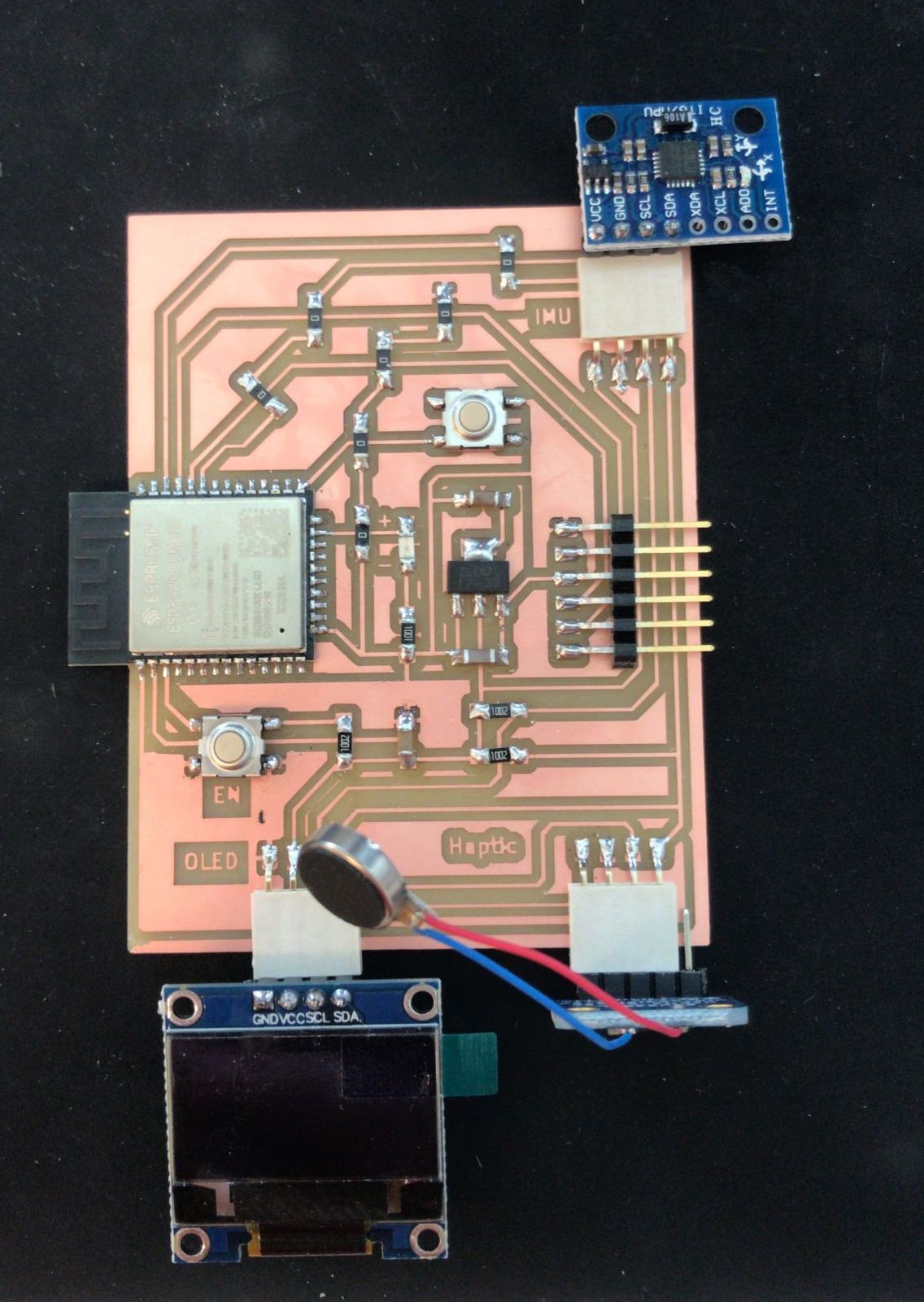
Testing
1) Test the Accelerometer/Gyroscope module and OLED display:
2) Test the Haptic Controller module:
Group Assignment
This week's group assignment is to probe an input device's analog levels and digital signals. For this assignement, I used the DS212 mini oscilloscope from our Home Fab Lab Kit to probe a hall effect sensor on the ELEGOO UNO board. To begin, I followed this YouTube tutorial to learn the basics of the device. I followed this tutorial for the set up.
I then connected the probe to GND of the Arduino board and the hall effect sensor. In Arduino IDE, I used digitalRead for digital signal detection and analogRead for analog signal detection.
Files
Please find below the files that I made for this assignment.
- KiCad files for ATtiny1614_ADXL343 input test (include schematic and PCB files)
- Traces and Interior
- Rectangular Shape (.zip folder of SVG and PNG files)
- Tree Shape (.zip folder of SVG and PNG files)
- G-code files for milling FR1 board (traces, interior)
- Prepared .ai files for fiber laser cutting (tree board, rectangle board)
- Arduino Sketch