
This work is licensed under a Creative Commons Attribution-NonCommercial-ShareAlike 4.0 International License
Week 6: Electronics Design
Mar 9, 2021Summary
This week's assignments
- Group assignment: (**Please refer to my Assignment 2 "Using Test Euipments" section**)
- Use the test equipment in your lab to observe the operation of a microcontroller circuit board (in minimum, check operating voltage on the board with multimeter or voltmeter and use oscilloscope to check noise of operating voltage and interpret a data signal) ✔
- Document your work (in a group or individually) ✔
- Individual assignment: (**Please refer to my Assignment 1 section**)
- Redraw one of the echo hello-world boards or something equivalent, add (at least) a button and LED (with current-limiting resistor) or equivalent input and output, check the design rules, make it, test it:
- Document what you have learned in electronics design ✔
- Explain problems and how you fixed them, if you make a board and it doesn't work; fix the board (with jumper wires etc) until it does work ✔
- Load a program and test if your board works ✔
- Include original design files (Eagle, KiCad, SolidWorks PCB, - whatever) ✔
- Include a "hero shot" of your board ✔
Resources Used
- Software: KiCad, mods - cba edition, Arduino IDE
- Hardware: Roland SRM-20, Power Supply, Multimeter, Oscilloscope
Skills Gained
- circuit design, microcontroller test
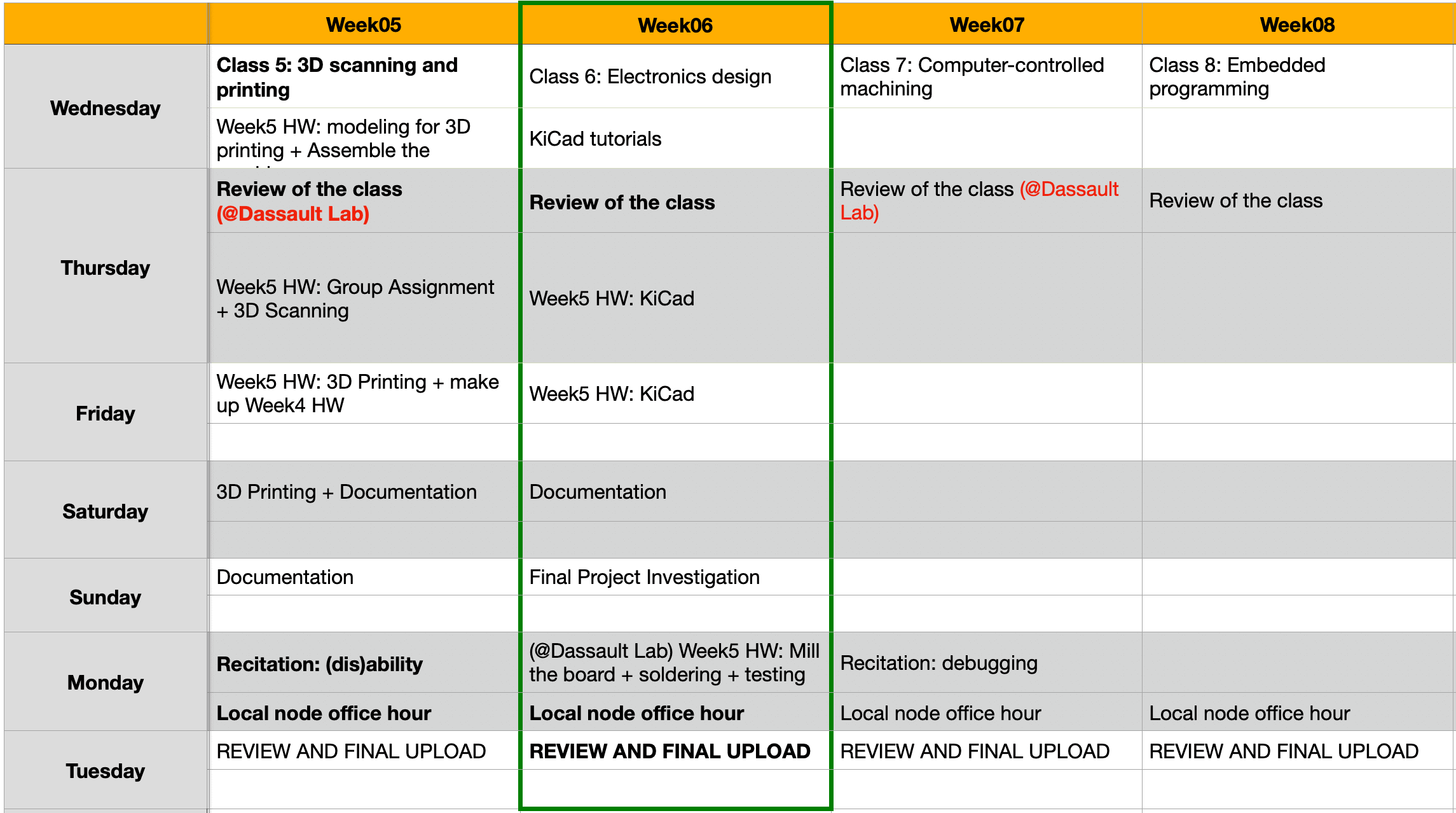
My Weekly Schedule
Getting Started with KiCad
During the Global Lecture on Wednesday, Neil introduced two main software that we could use to make PCBs, KiCad and EAGLE. After doing some research, I decided to dive into KiCad mainly because of the integrated 3D Viewer feature, which allowed me to visaulize the end result after making the 2D schematic and footprint of the board. I saw this as a great help to me during the soldering process.
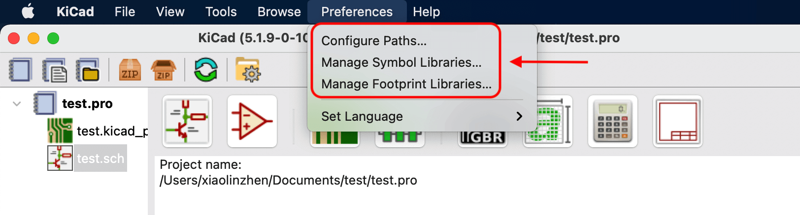
To begin, I downloaded the latest KiCad stable release (KiCad 5.1.9) on my Mac. I also git clone the Fab electronics component library to my ~/Library/Application Support/kicad/library folder, and followed the README.md file to do the following:
- Add the
fab.libfile to the Symbol Library - Add the
fab.prettyfile to the Footprint Library - Configure the path of
/Library/Application Support/kicad/library/fabwith the variable name FAB - This will allow me to see the 3D shapes of the electronics components after making the schematic and footprint of my PCB
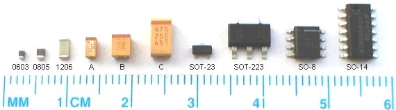
The next step for me was to explore video courses and interactive practice sessions on KiCad. For this, I went through a few YouTube tutorials (1, 2 and 3) by Kris from Aalto FabLab (Espoo, Finland) to get myself familiar with the basics. I found these tutorials very helpful because they were geared towards Fab Academy. From the tutorials, I have learned the best practices in PCB designs, what's more, I have learned how to create a symbol / footprint for a specific component, where to assign the footprint for the 1206 package size for SMD (the package size that Fab Academy uses), and how to define the 0.4 mm (1/64") track width for milling the traces of the PCB.
Assignment 1: Hello-World Boards
Designing in KiCad
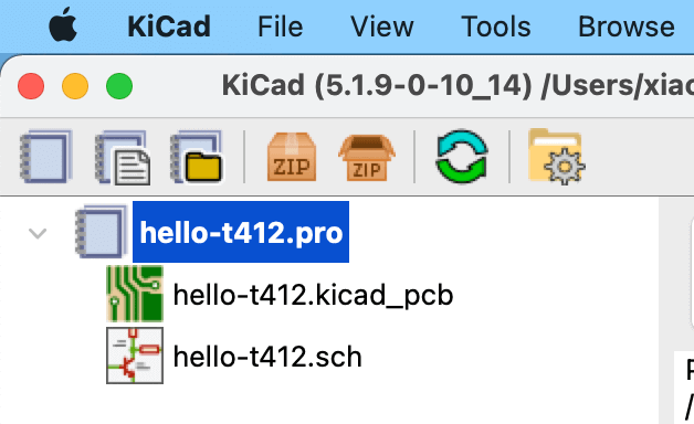
- I created a new project (File > New > Project) and renamed it as
hello-t412, and KiCad would generate two files for me, one was the schematics file (.sch), and the other was the PCB file (.kicad_pcb). We started with the schematics file so I double clicked to open it. - Here are some tools that I found helpful when working with the schematic file.
- Show/Hide grid - I preferred the grid activated.
- Set unit to mm
- Place symbols - Add electronics components symbols (keyboard shortcut A )
- Place power port - Add power source (i.e. GND, VCC, VDD...etc.)
- Place wire - Add the wires (keyboard shortcut W )
- Select item - This allowed me to use the keyboard shortcuts to copy (keyboard shortcut C ), rotate (keyboard shortcut R ) and edit (keyboard shortcut E ) when I hoveredover a symbol
- Place no connection flag - Some pins didn't need connection and I would need to cross it out. If I didn't mark the X for that pin, I would receive an error during the electrical rule check step.
- Place net label - This feature allowed me to add text on the wire without having to connect two pins. Similar to the place no connection flag tool, if I didn't place a text on an "open wire", I would receive an error during the electrical rule check step.
- Create, delete and edit symbols - Sometimes I needed to create my own symbol for a component because I couldn't find a symbol that had the same information as the board.
- Annotate schematic symbols - This tool ensured me to have no question mark on my symbols
- Perform electrical rules check - This allowed me to make sure I had no open circuit, short circuit...etc.
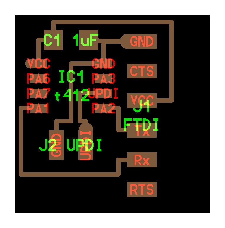
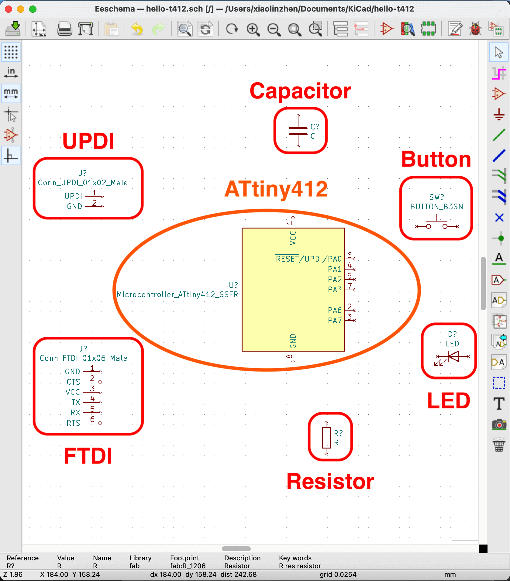
- When working with the schematics file, I referred to the board.png to make sure I have selected the correct symbol. This was important becasue if we selected a symbol that did not have the same information, the final board would not work.
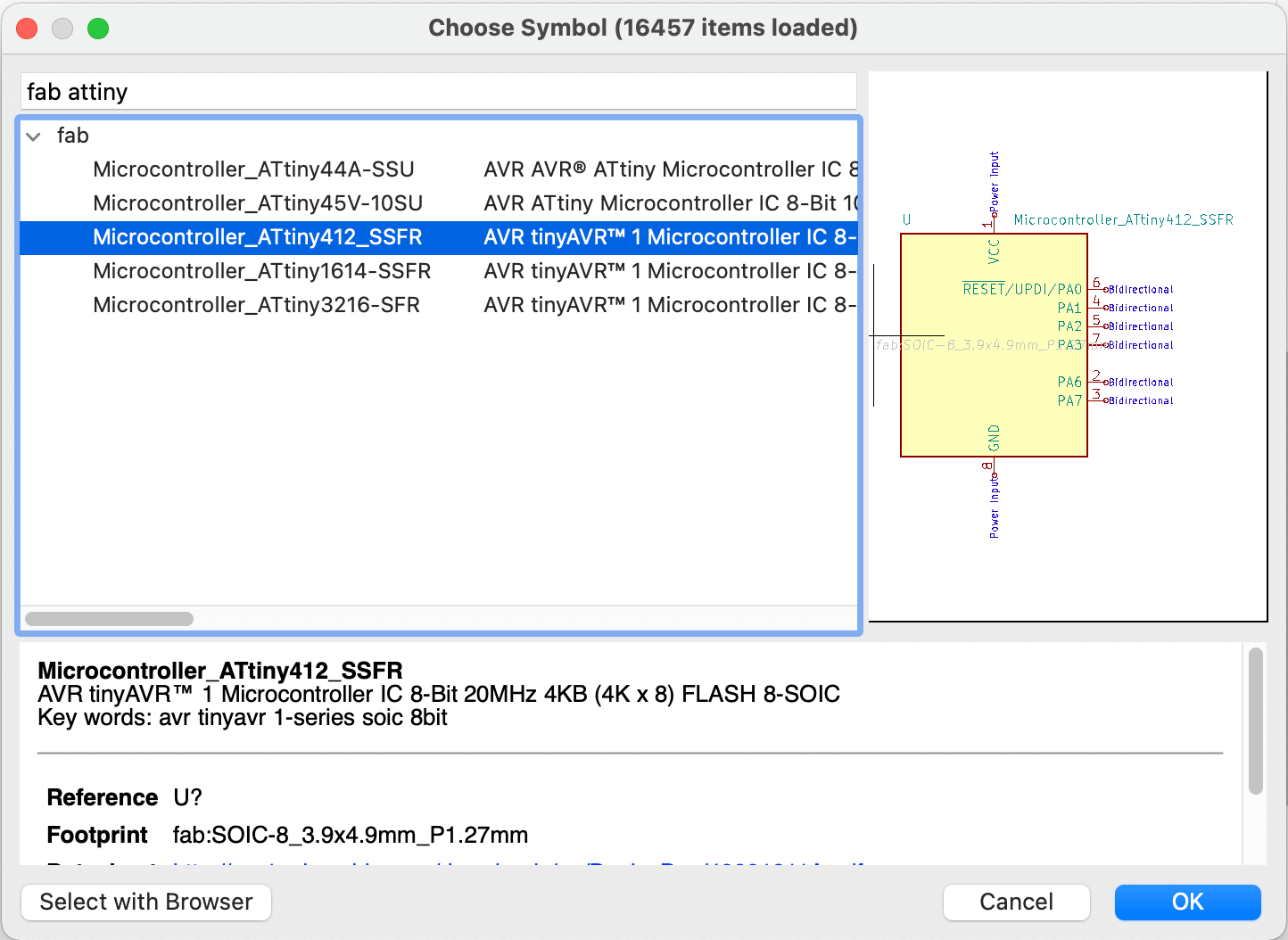
- I started by adding the microcontroller (IC). In this case, I had the ATtiny412. To add a component, I clicked the keyboard shortcut A to bring up the Place symbols search page. As I was using the Fab electronics component library, my keywords would begin with "fab" as it helped narrow down the list. For example, I typed "fab attiny" to search for the ATtiny412 microcontroller.
- Then, I repeated the previous step to add the other components.
- UPDI - type "fab updi".
- FTDI - type "fab ftdi".
- Resistor - type "fab res".
- Capacitor - type "fab capa", and this would provide two options: "unpolarized capacitor" and "polarized capacitor". In this case, the capacitor that I would be using to fileter the current for microcontroller was a bypass capacicator, I selected the "unpolarized capacitor". If I were to work with motor controller, amplifier, or audio filters, then I would select "polarized capacitor".
- Button - Since the assignment required us to add a button, I used "fab button" in my search, and selected the "B3SN" button type as suggested.
- LED - The assignment also required to have an LED, so I used "fab led" in my search.
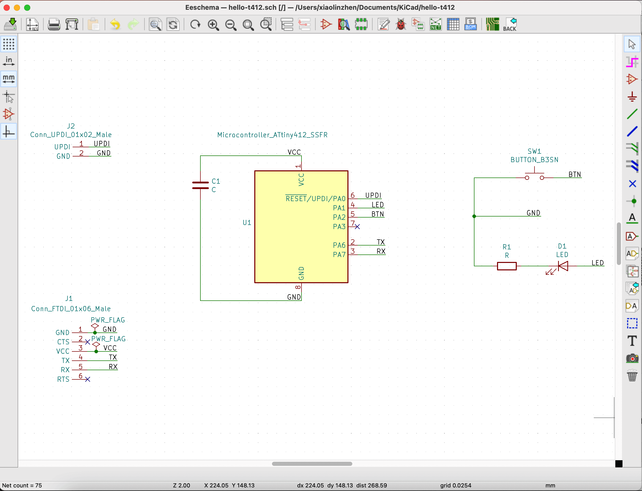
- After all the components were added, it was time to connect them with wires. For this, I activated the Place wire function by first hovering over the circle of a component, then clicking the keyboard shortcut W , and started my routing process, I double clicked to finish wiring.
- In this process, I used the board.png to help with my routing process.
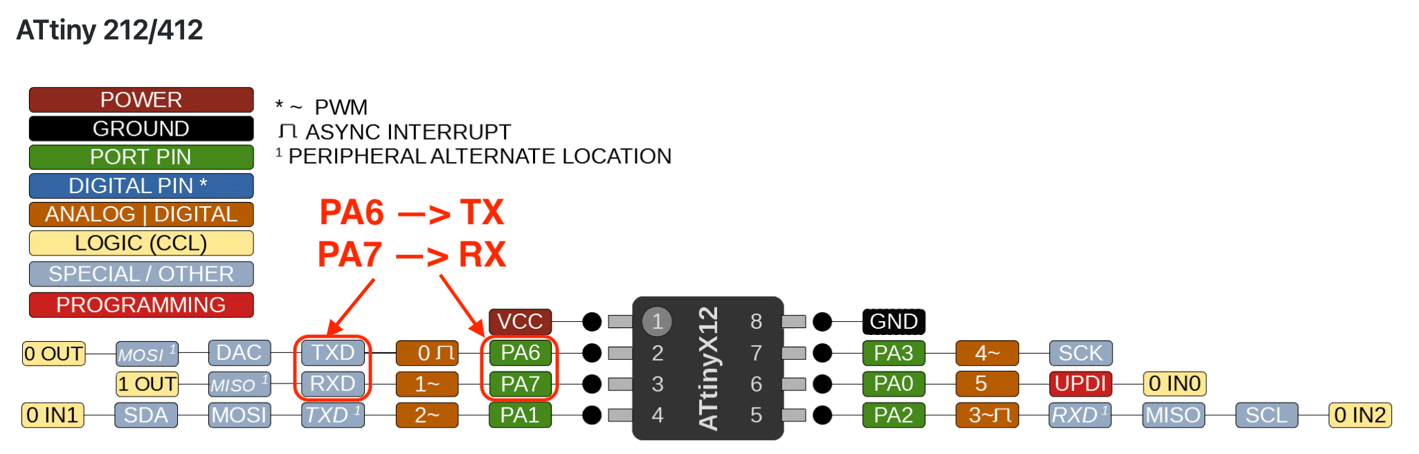
- When making the connections for the "TX" and "RX" between the FTDI and the ATtiny412, I referred to this megaTinyCore image to make sure I selected the right pins, in this case, PA6 was for "TX", and PA7 was for "RX". After connecting the wires,
- I used the Place no connection flag and Place net label tools to cross out / label some wires to avoid open circuit.
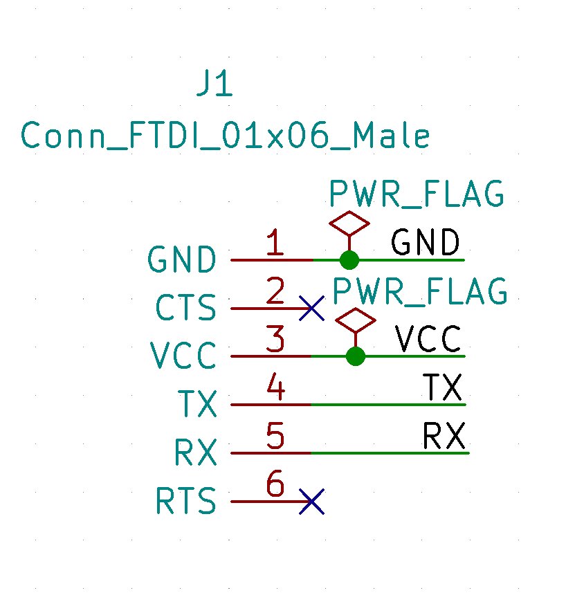
- Here is a special symbol to add: PWR_FLAG - type "pwr" in the Place Symbols search bar.
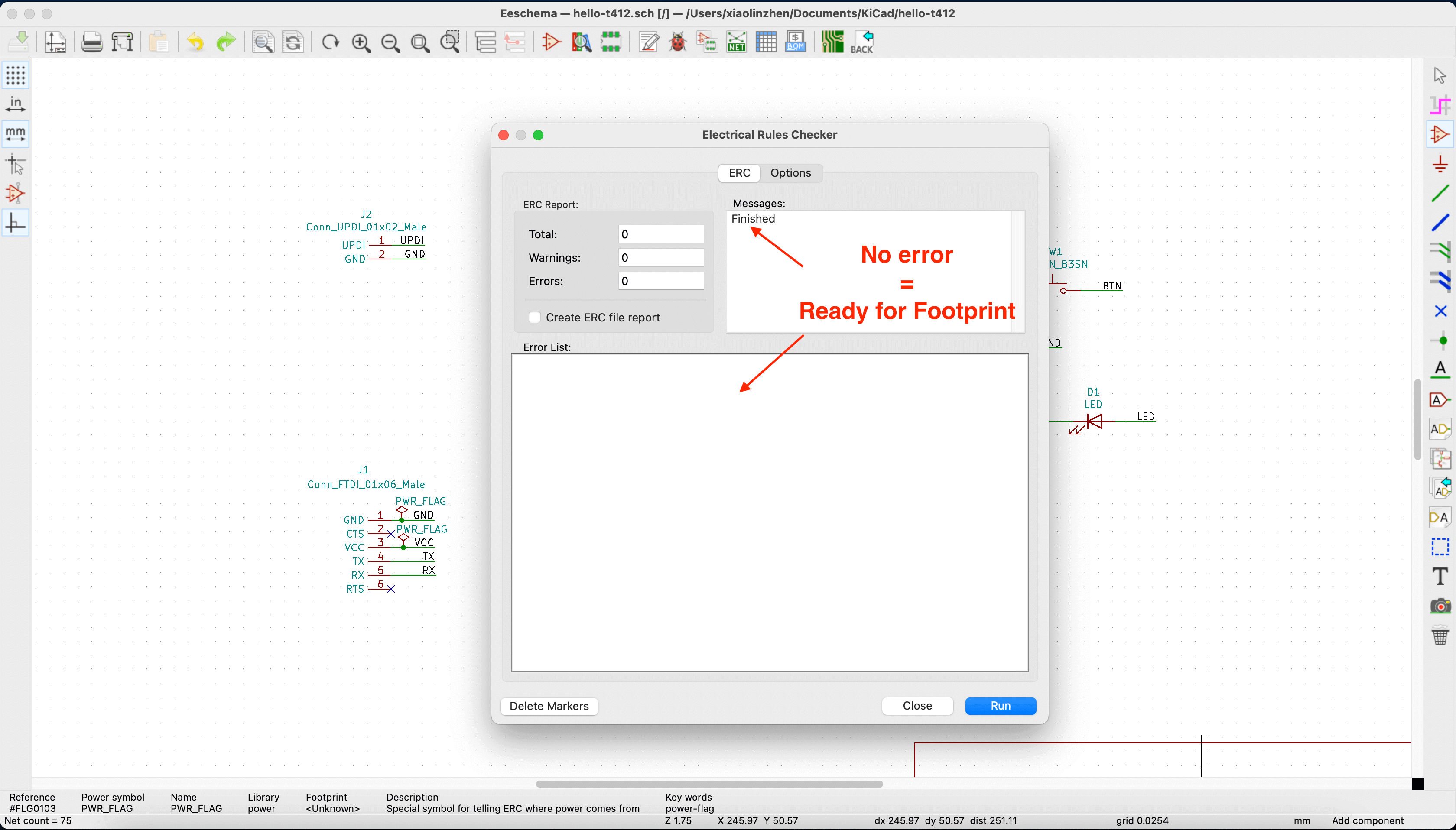
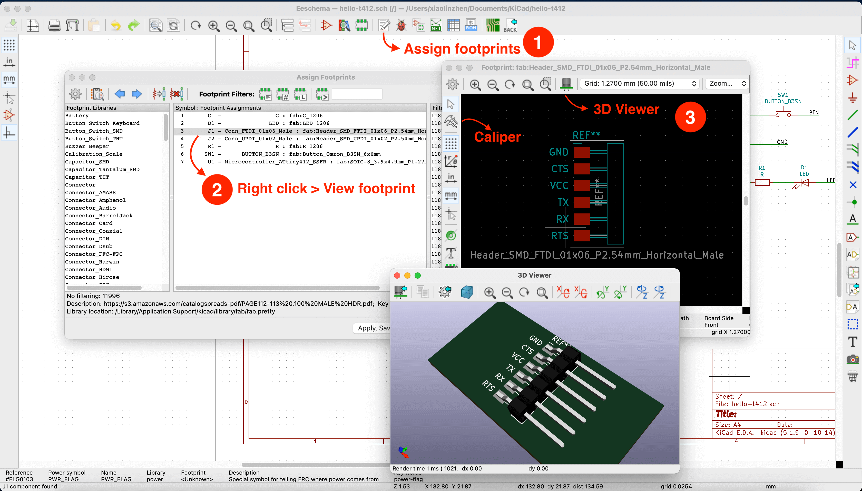
- Next, I ran the Annotate schematic symbols tool to replace the question marks with numbers (i.e J? --> J1 or J2, depending on the order of placement in the Place symbols step), and then ran the Perform electrical rules check tool to check for mistakes. When there was no mistake, I then clicked the Assign Footprints button, according to Kris, usually we would need to assign the footprints manually for each symbol in this step, but since we were using the "Fab electronics component library", the footprints should be assigned for us already. The footprint also allowed us to use a caliper to measure the component, and visualized the component in the 3D viewer
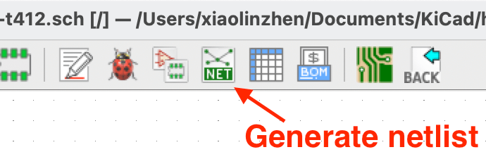
- After that, I clicked the Generate netlist icon and placed the .net file in the same folder as the other files of the same project. This step was to create electrical connections between the components on the circuit board.
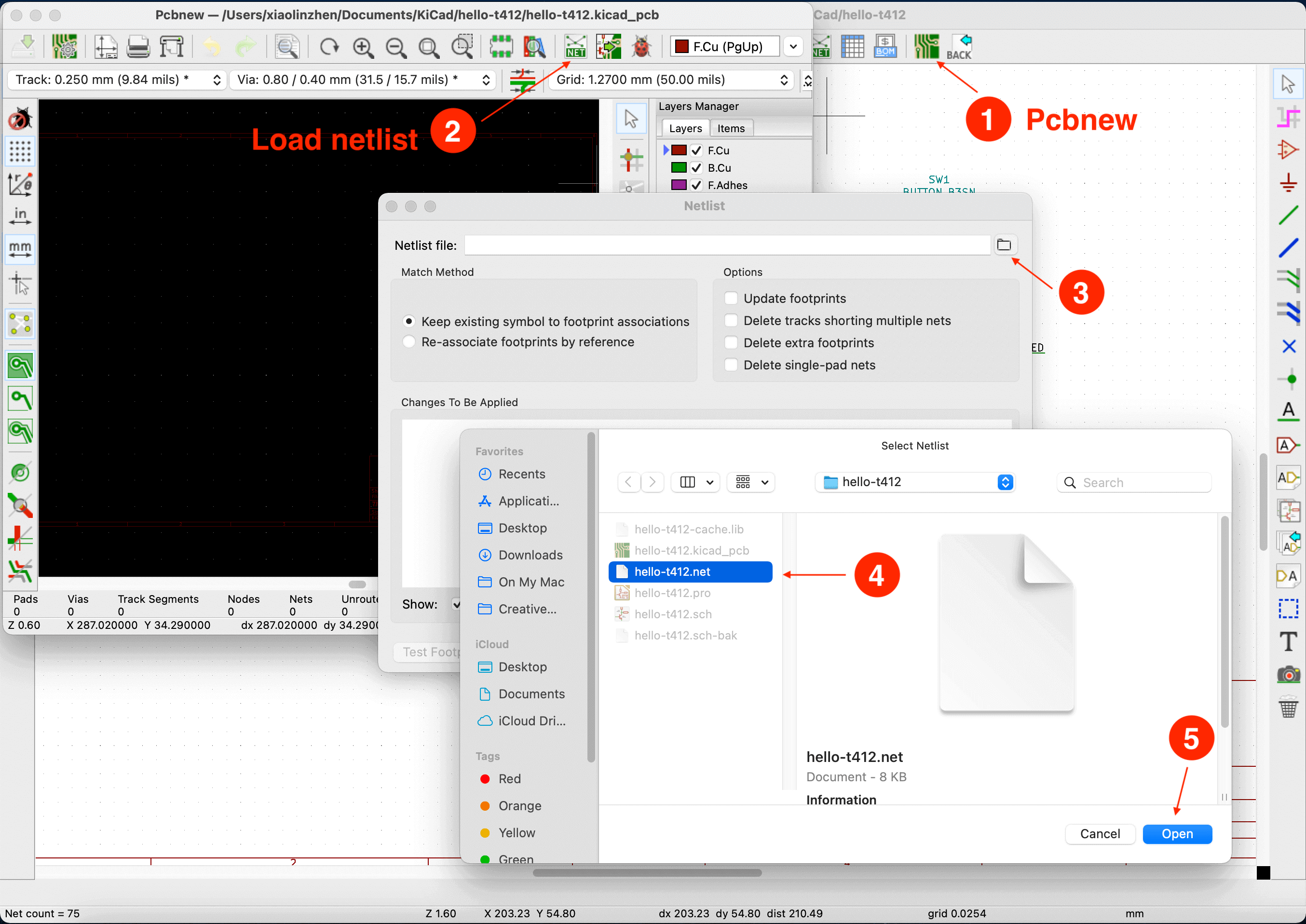
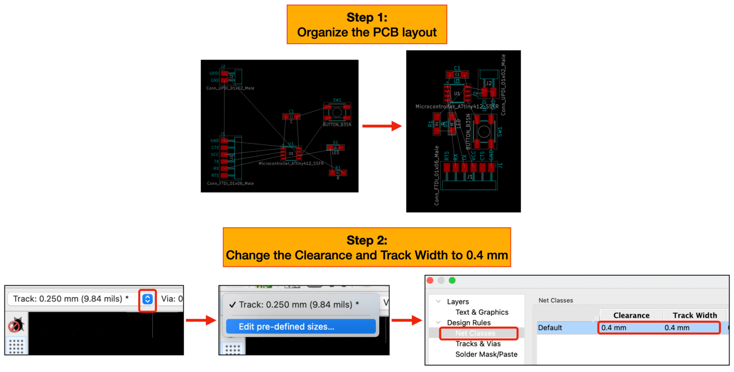
- After generating the netlist, I moved onto the PCB part of the program by clicking Pcbnew button. In here, I loaded the netlist file (.net) to realize the PCB layout, which still looked unorganized at this moment.
- I used the keyboard shortcut R (Rotate) and M (Move) to adjust the positions of the component for the PCB layout. I learned that, in order to achieve for better filtering performance, I should place the capacitor as close to the microcontroller as possible. I also adjusted the Clearnace and Track Width and the Net Classes to be 0.4 mm.
- Next, I connected the components with the Route track tool. As Neil said in the class, the PCB drawings are hierarchical parametric drawings, so Kris gave us some pointers:
- Try to connect the coomunication lines first (UPDI -> UPDI, LED -> LED, BTN -> BTN)
- Route the voltages, but leave the GND open for the last step, which is going to help to denoise the board (i.e. protect the connections from interference)
- Connect TX and RX
- Avoid 90° angle for routing
- Use the drag tool (Keyboard shortcut D ) to reposition the wire.
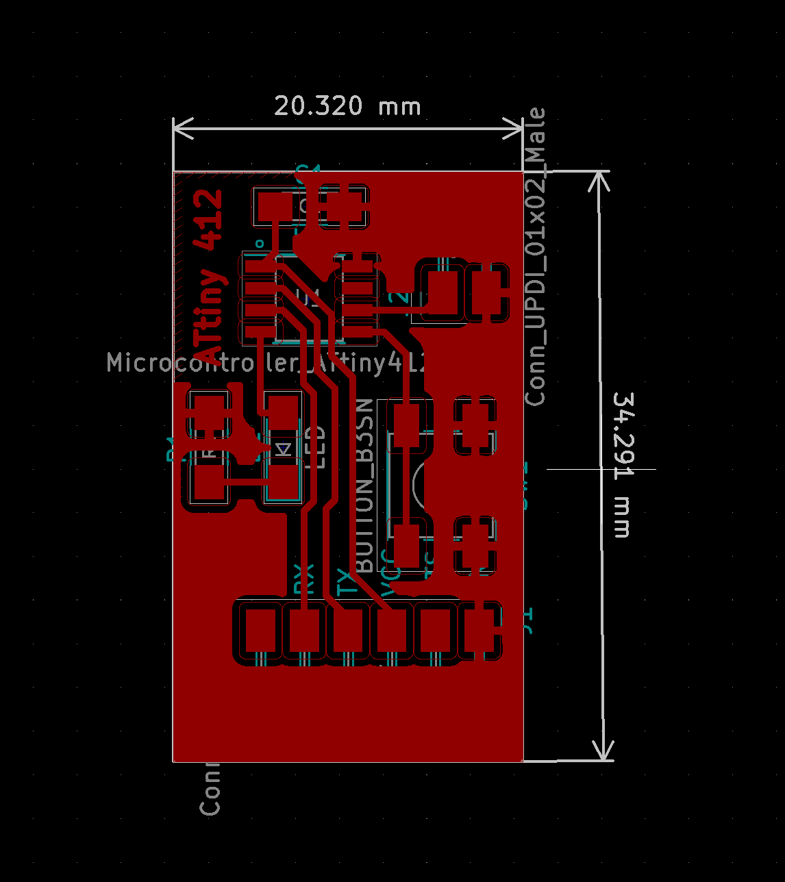
- After routing the components except for the GNDs, it was time to draw the outline of the board. To begin, I changed the grid to 0.5 mm. Then, I used the Add graphic lines tool to draw the outline of the board. For this, I needed to make sure all the lines were connected. After that, I used the Add dimensions tool to check the size of the board. The dimensions would need to be removed afterwards.
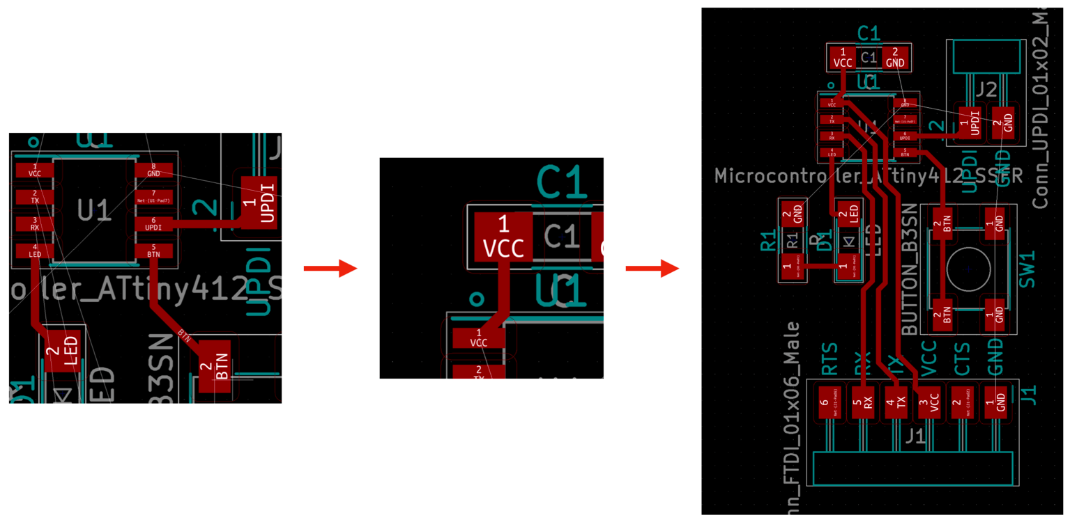
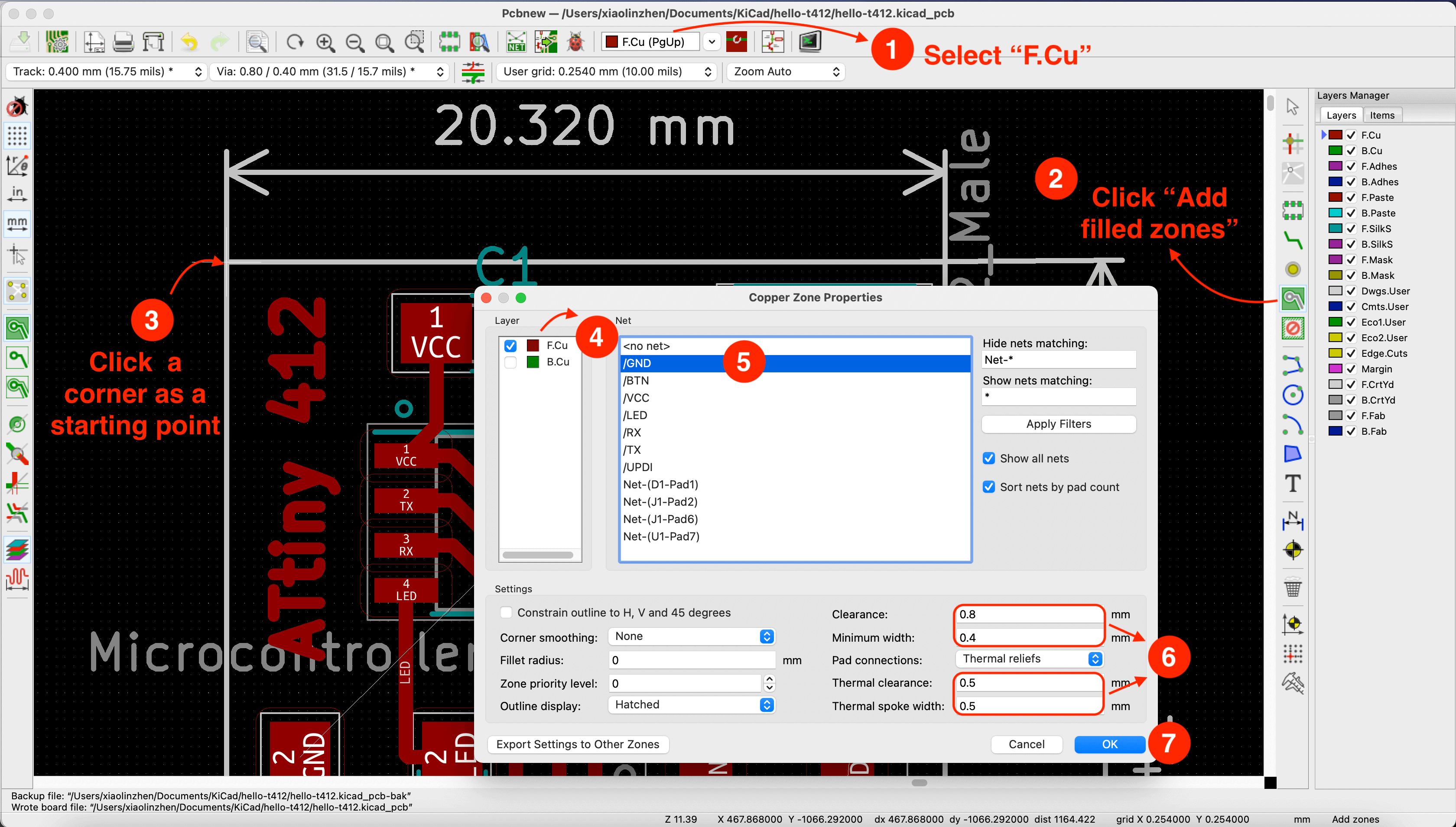
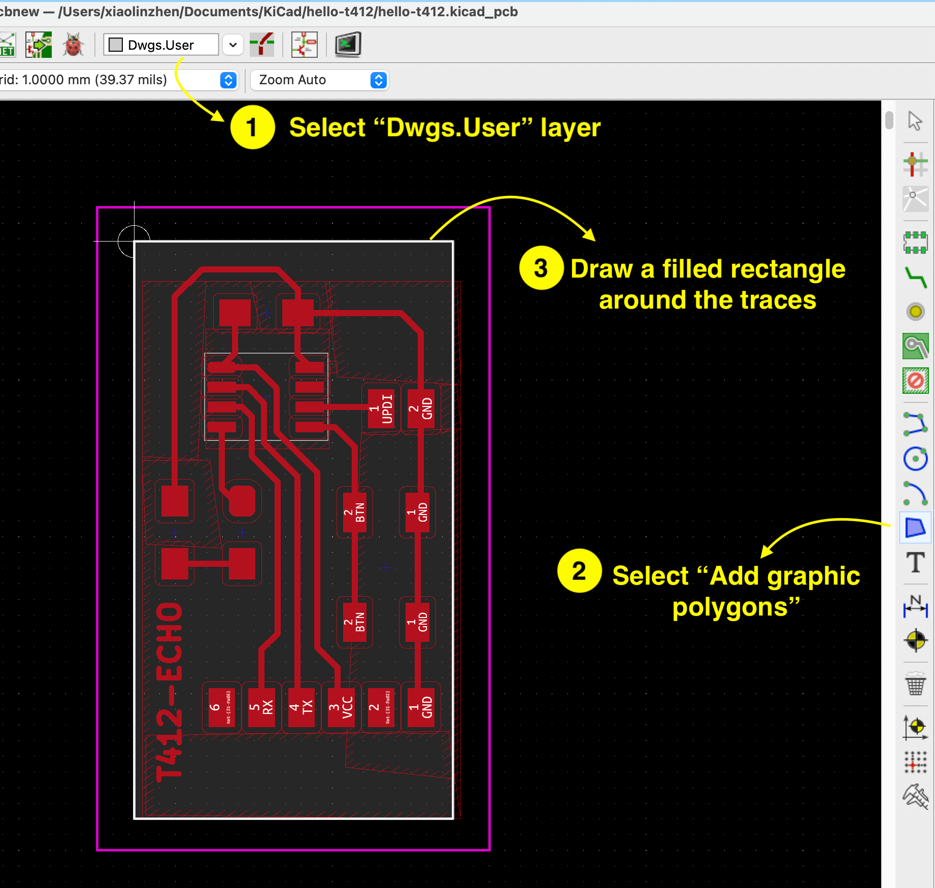
- Then, I was ready to connect the GND. To begin, I needed to select the correct layer, which was the F.Cu.
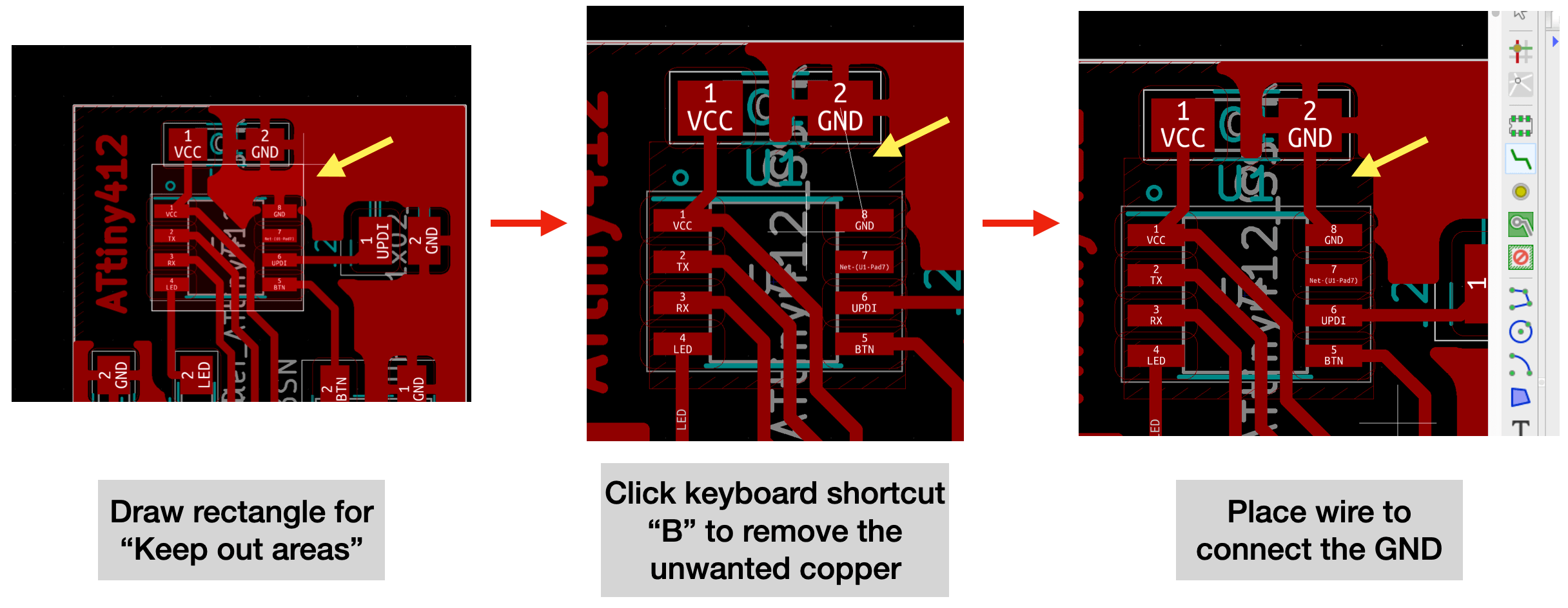
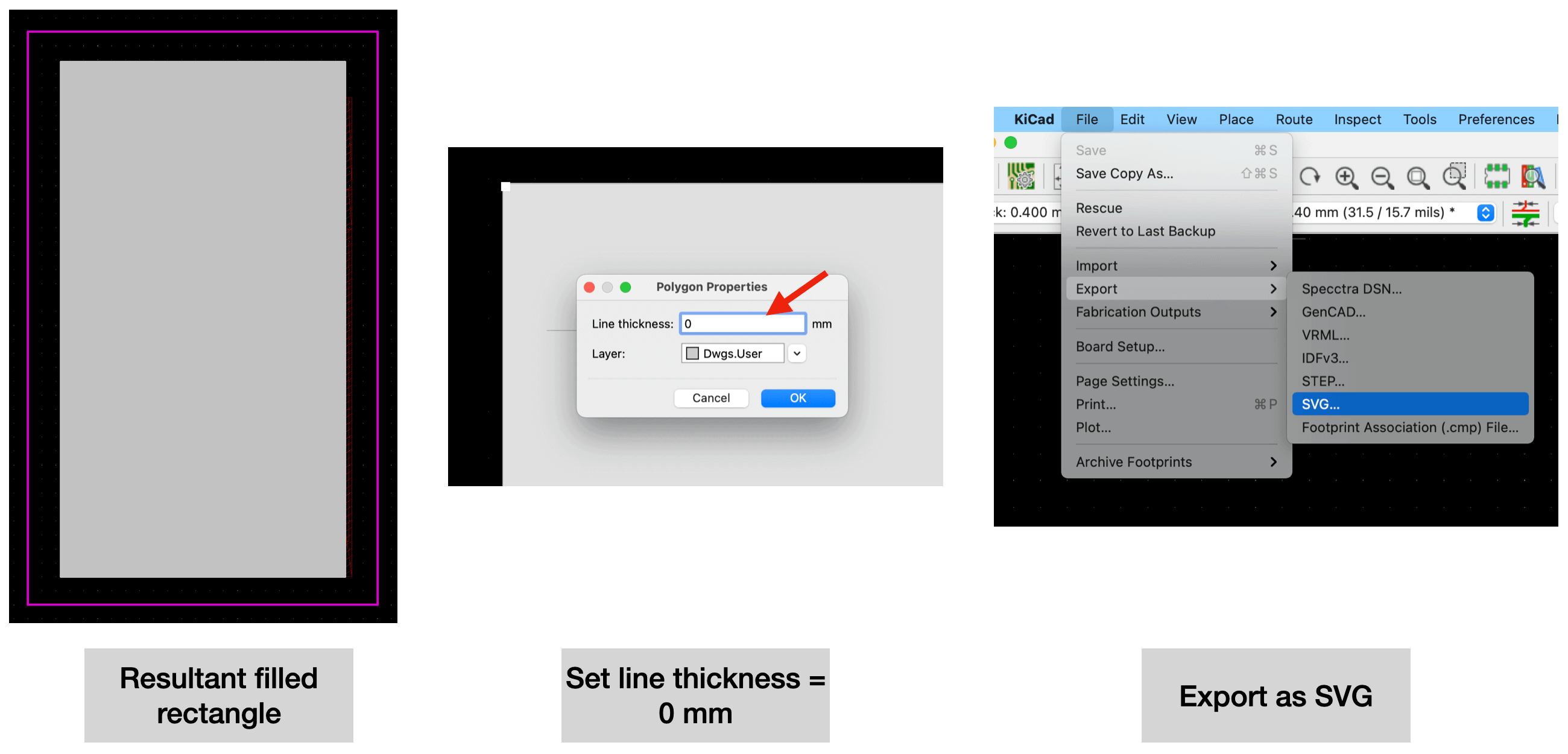
- I followed the workflow in image 1 below to connect all the unconnected GND together, and the result is shown in image 2 after drawing the filled rectangle on the edges.
- Make sure the copper fill was going to represent the GND (ground net) and end up at the F.Cu layer
- Specify the clearance = 0.8 mm; width = 0.4 mm; and thermal clearnace = 0.5 mm. According to Kris, the thermal was 0.5 mm becasue it had to be bigger than their minimum width, which was 0.4 mm in our case.
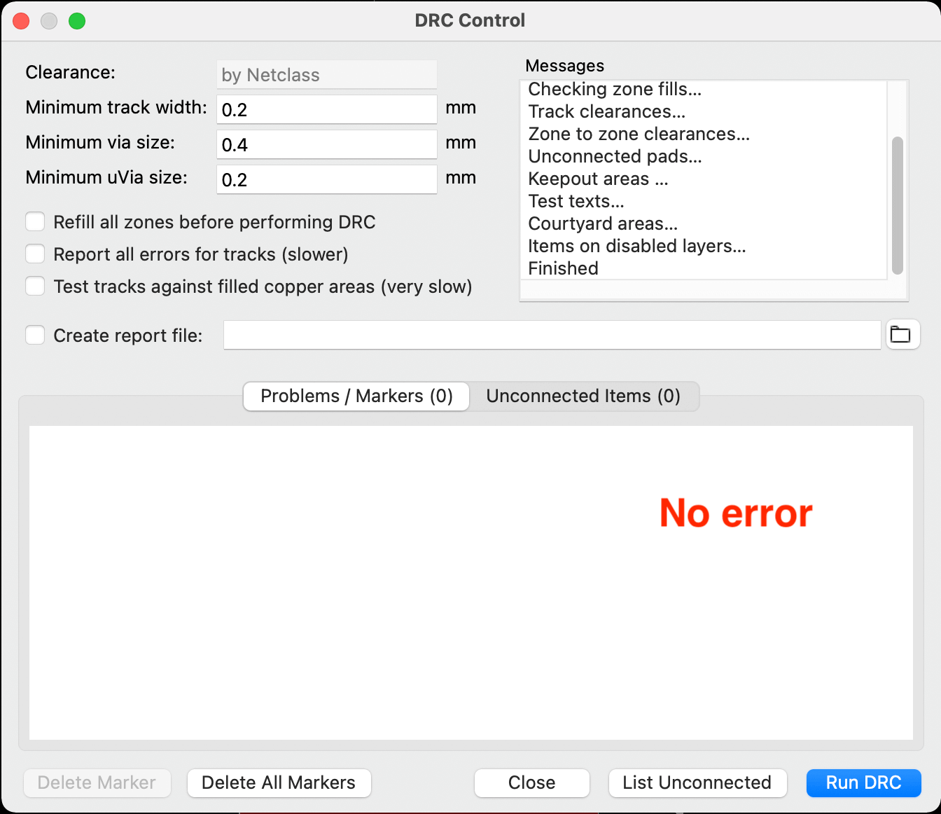
- After that, I ran the Peform design rules check (the bug) to check for mistakes.
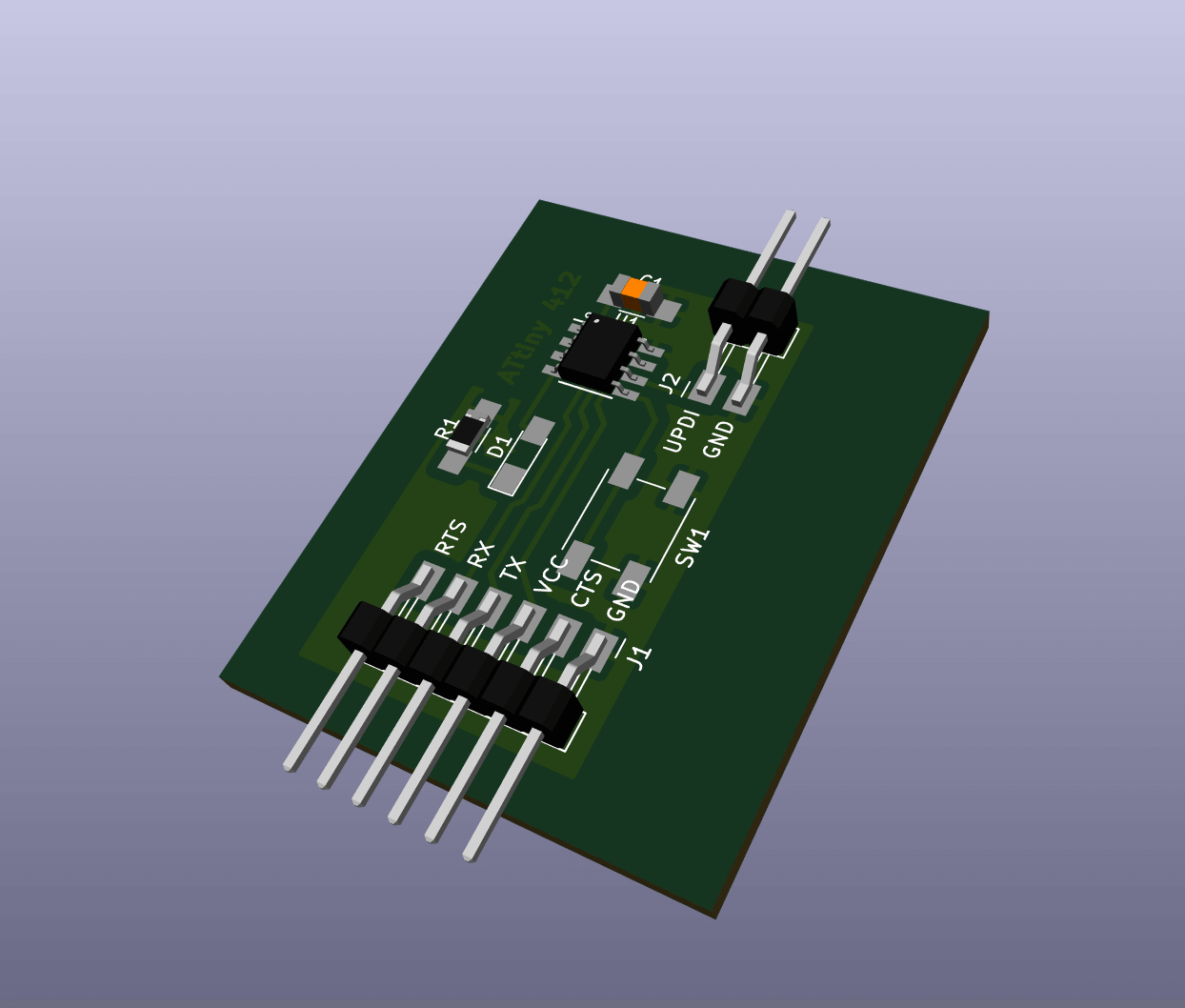
- At this point, I was excited to see how my board would look in the 3D Viewer, so I pressed Option + 3 to enable the 3D Viewer... TADA! It looked so pretty!! 😍 But wait, something was wrong...🤔 the board looked bigger than I thought, and I realized it was because I hadn't removed the dimensions, and also some texts were ouside the fabrication areas - if I milled the board like this, I would waste some FR1 material.
- Learning from my mistake, I then used the move tool (keyboard shortcut M ) to bring in the texts that were placed outside the filled red rectangle. I also deleted the dimensions before moving onto the next step in Kris' tutorial.
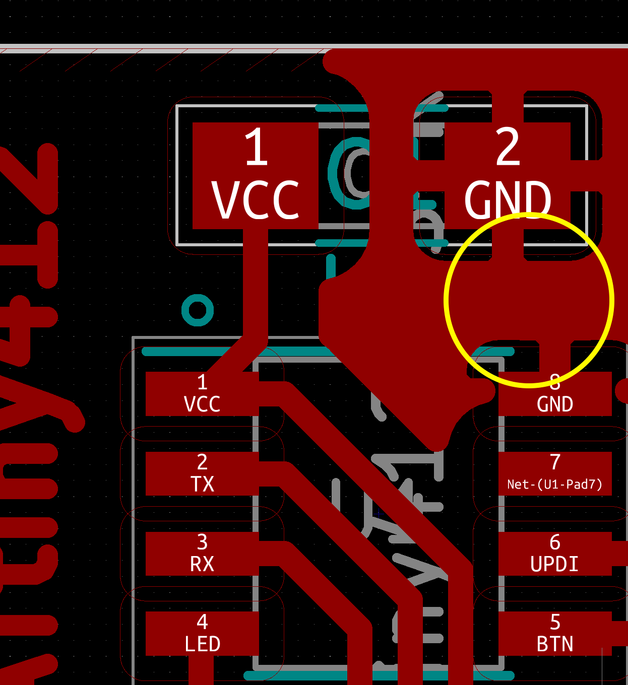
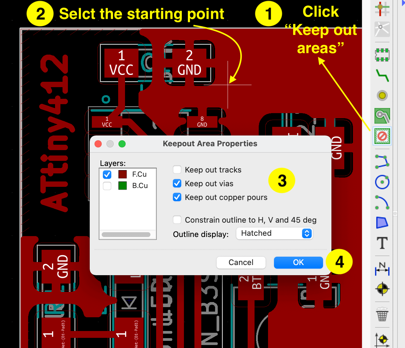
- Next, I followed the steps below to use the Keep out areas tool to specify some areas where the copper shouldn't appear at all (i.e. remove the unwanted ground connection between the capacitor and the microcontroller).
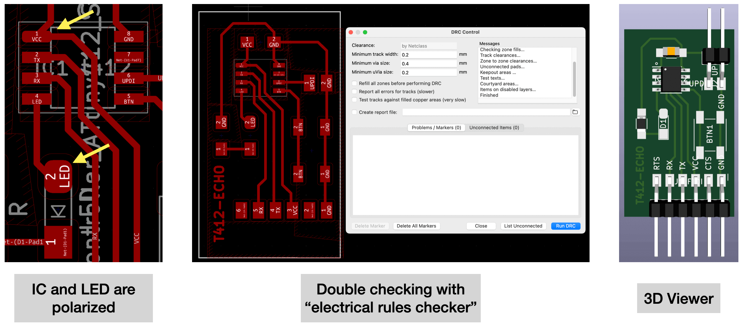
- I spent some time doing clean up on the copper with the same trick, and created a reminder for myself on the polarity of the IC and LED components using rounded rectangle. After that, I ran the Perform electrical rules check tool again to make sure my traces were not too close to the edge. Then, I unchecked the F.SilkS (front silk layer), F.CrtYd (front courtyard layer) and F.Fab (front fab layer) as we were not going to fabricate these. And here is how my final board looked.
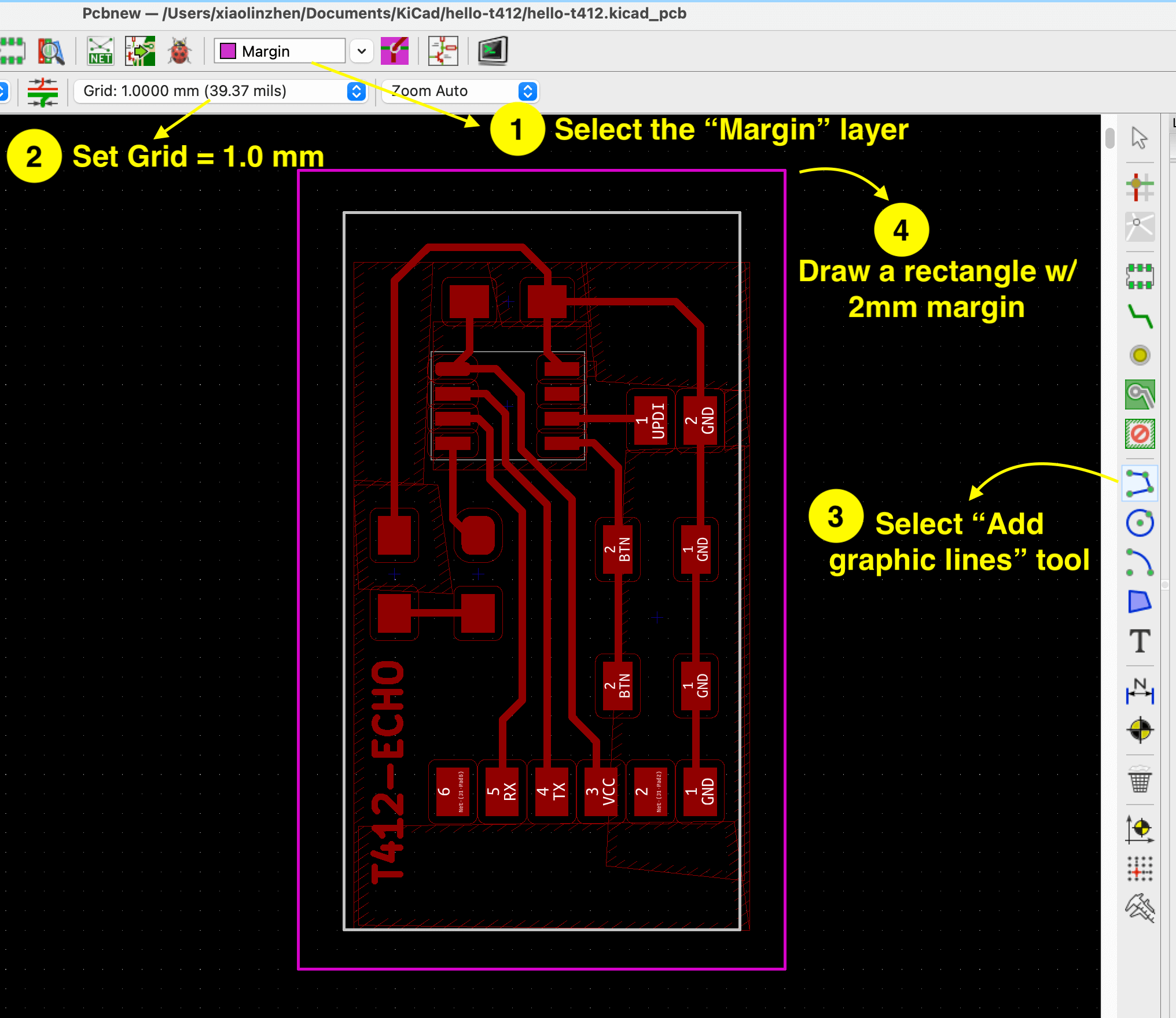
- At this point, I was ready to export my files as SVG to generate the G-code files in mods. I followed the workflow below to use the Margin and Dwgs.User to draw the interior. According to Kris, it would be easier for mods to figure out the path if we set some margin (here we gave a 2mm margin) for the outline SVG file.
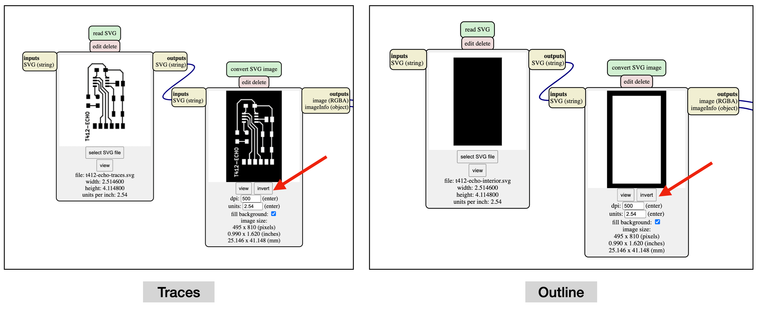
- After that, I was ready to export my SVG files for the traces and the interiors. I saved my SVG files in the same directory as the other files for this assignment, and renamed the filenames as "t412-echo-traces.SVG" (for traces file) and "t412-echo-interior.SVG" (for outline file), respectivelsy.
- Here is the top view of the board, with a 2 mm margin around the traces.
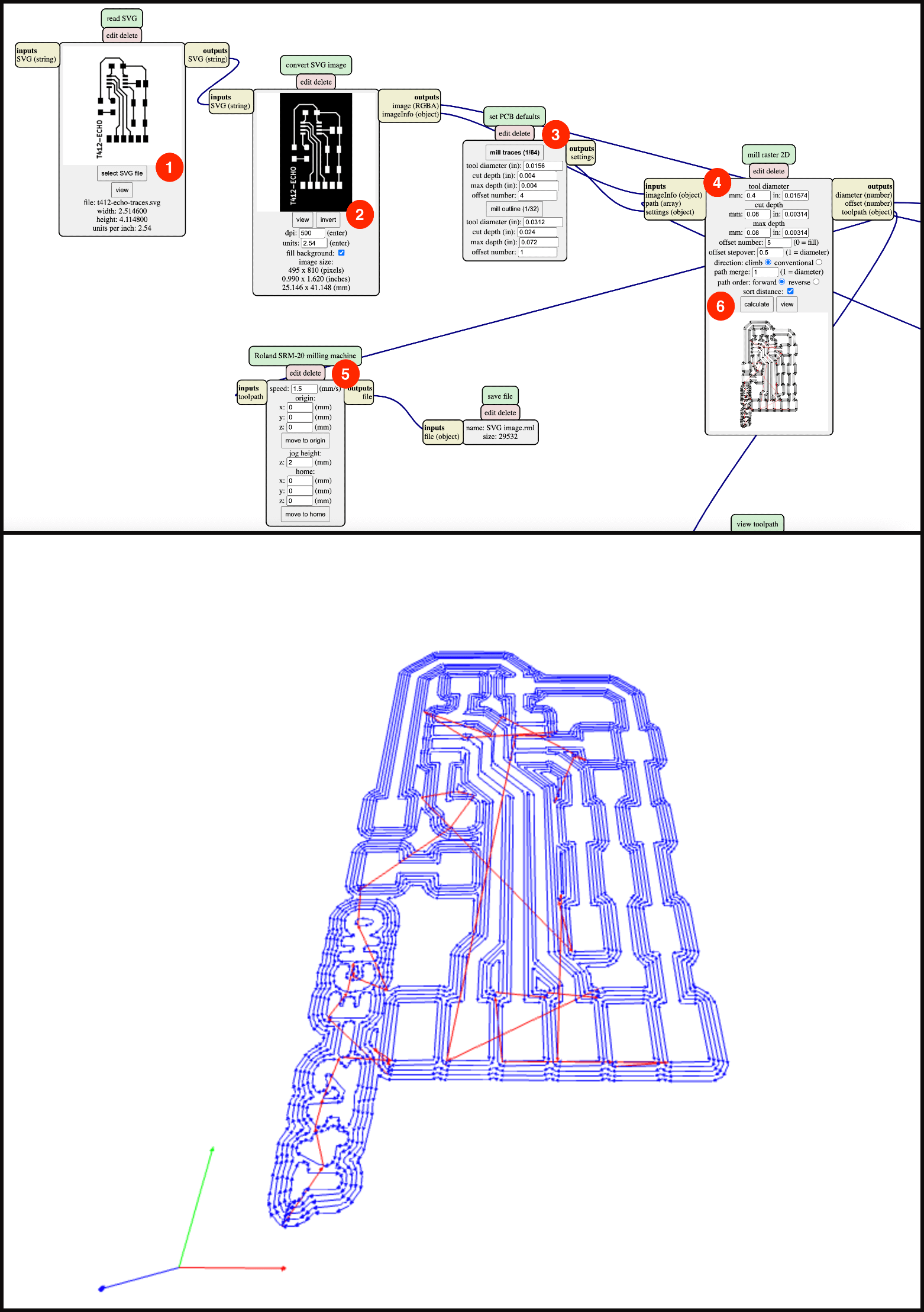
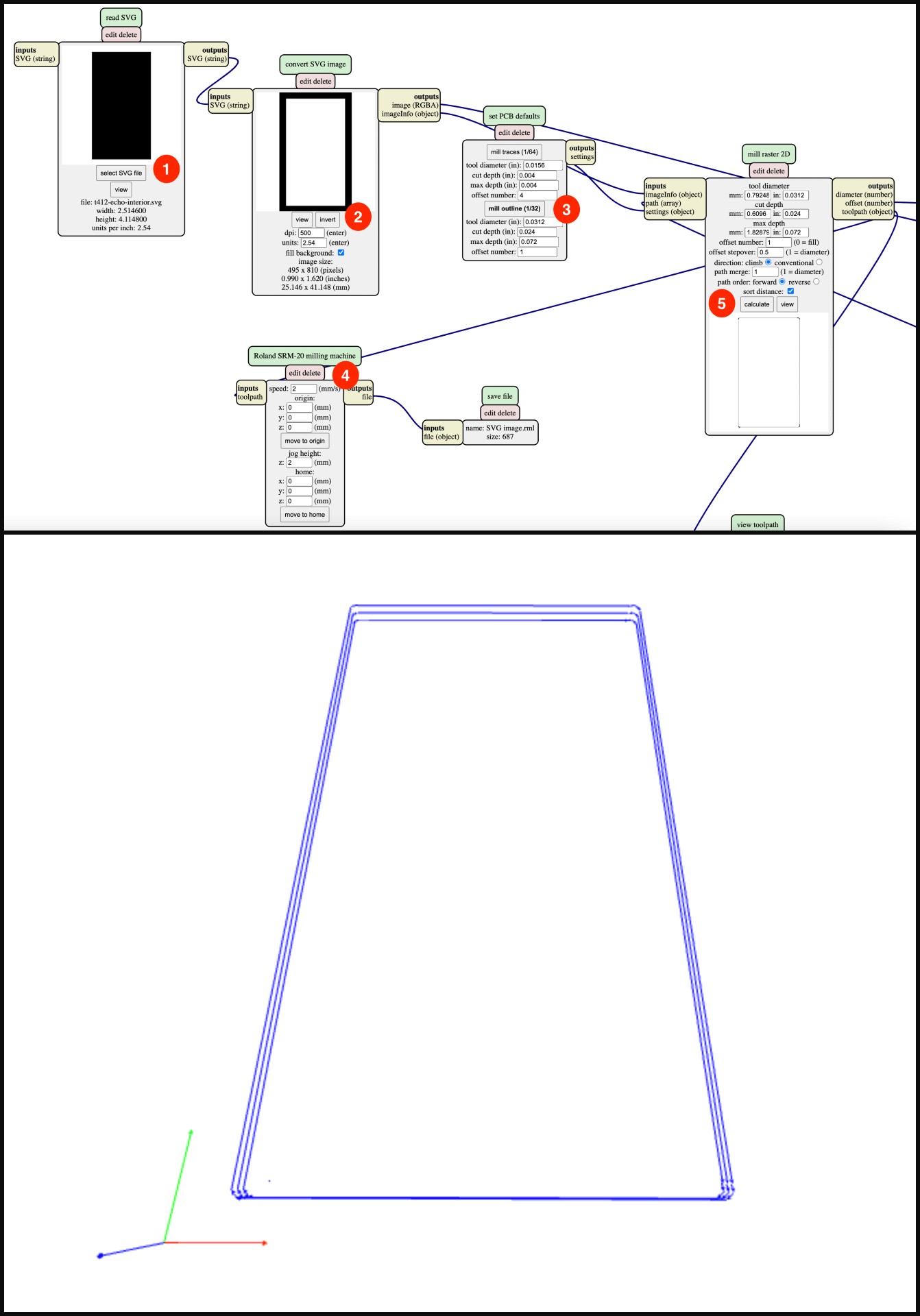
- Next, I generated my G-code files (.rml) for the traces and the outline using mods - cba edition. As the process was similar to what I did in my Week 4 documentation, I will be explaining in less detail in this week's documentation. One thing that I must was to invert the images before calculating the path for G-code.
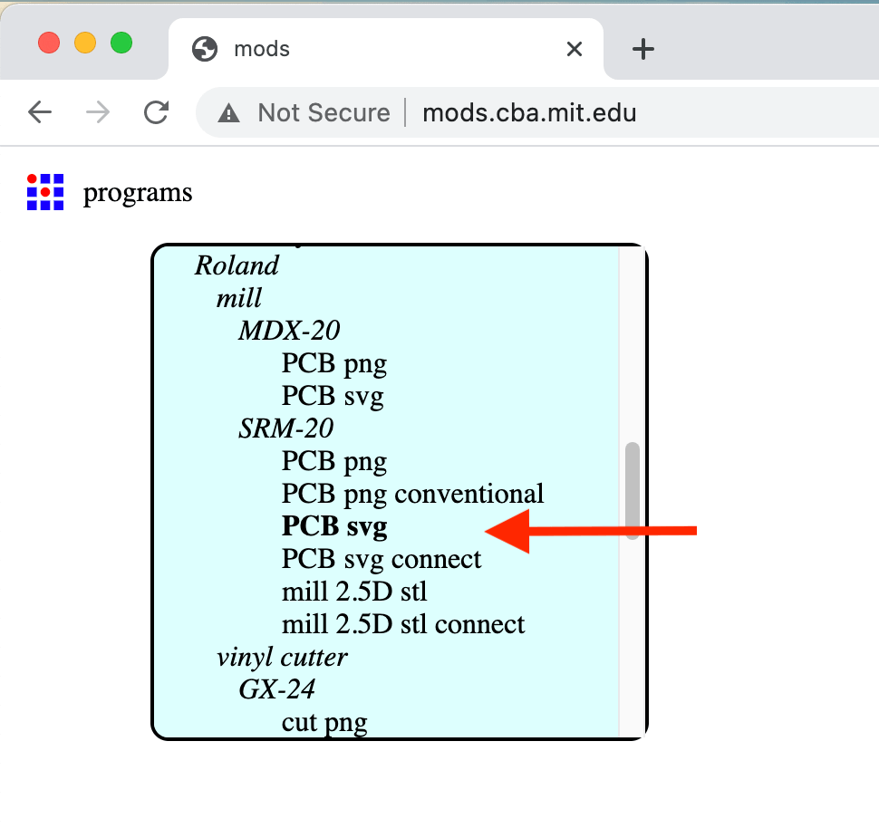
- Program: SRM-20 > PCB SVG
- Traces: (**make sure to invert**)
- Mill traces: 1/64" milling bit
- Tool Diameter: 0.4 mm
- Cut depth: 0.08 mm (I want the offset = 5)
- Max. depth: 0.08 mm (same as cut depth)
- Offset: 5
- Speed: 1.5 mm/s
- Origin (X/Y/Z): 0/0/0
- Home (X/Y/Z): 0/0/0
- Outline: (**make sure to invert**)
- Mill outline: 1/32" milling bit
- Use the default for: tool diameter / cut depth / max. depth / offset
- Speed: 2 mm/s
- Origin (X/Y/Z): 0/0/0
- Jog height: 2 mm
- Home (X/Y/Z): 0/0/0
.sch file and the .kicad_pcb file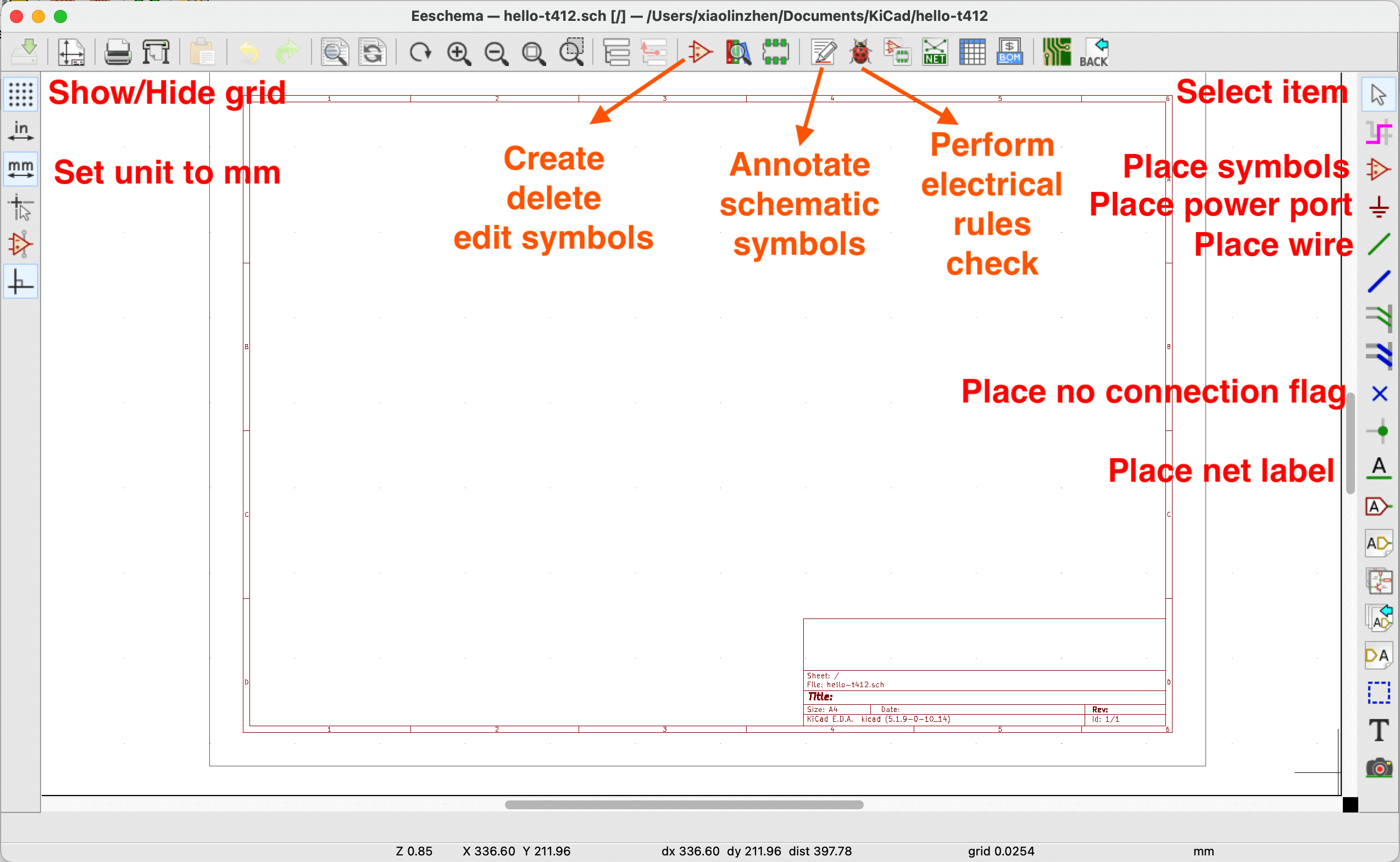
The PWR_FLAG was added after placing all the wires but before running the electrical rules check, I needed to add this symbol to state where the power came from. In this case, the power came from the FTDI, so I needed to place two power flags on the GND and VCC wires. If I didn't do this, I would receive the "Pin connected to other pins, but not driven by any pin" error during the "perform electrical rules check" step.
.kicad_pcb file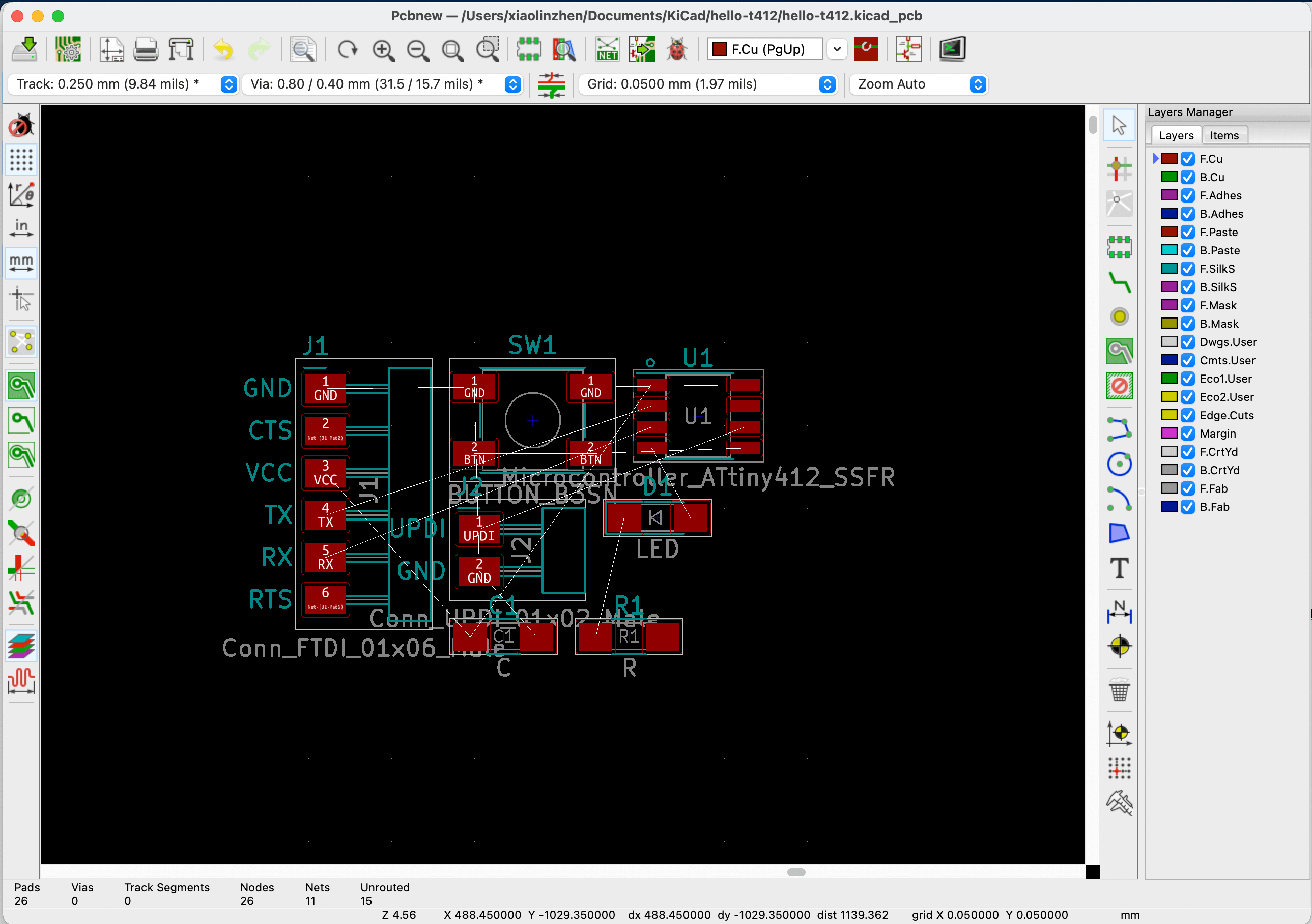
The Add dimensions tool helps users to make more compact PCBs if they want, but it also helps them to make sure the board is not oversized, i.e. I should design my boards to be smaller than 2.5" x 3.0" (63.5 mm x 76.2 mm) to accomodate the FR1 size that we have at the lab.
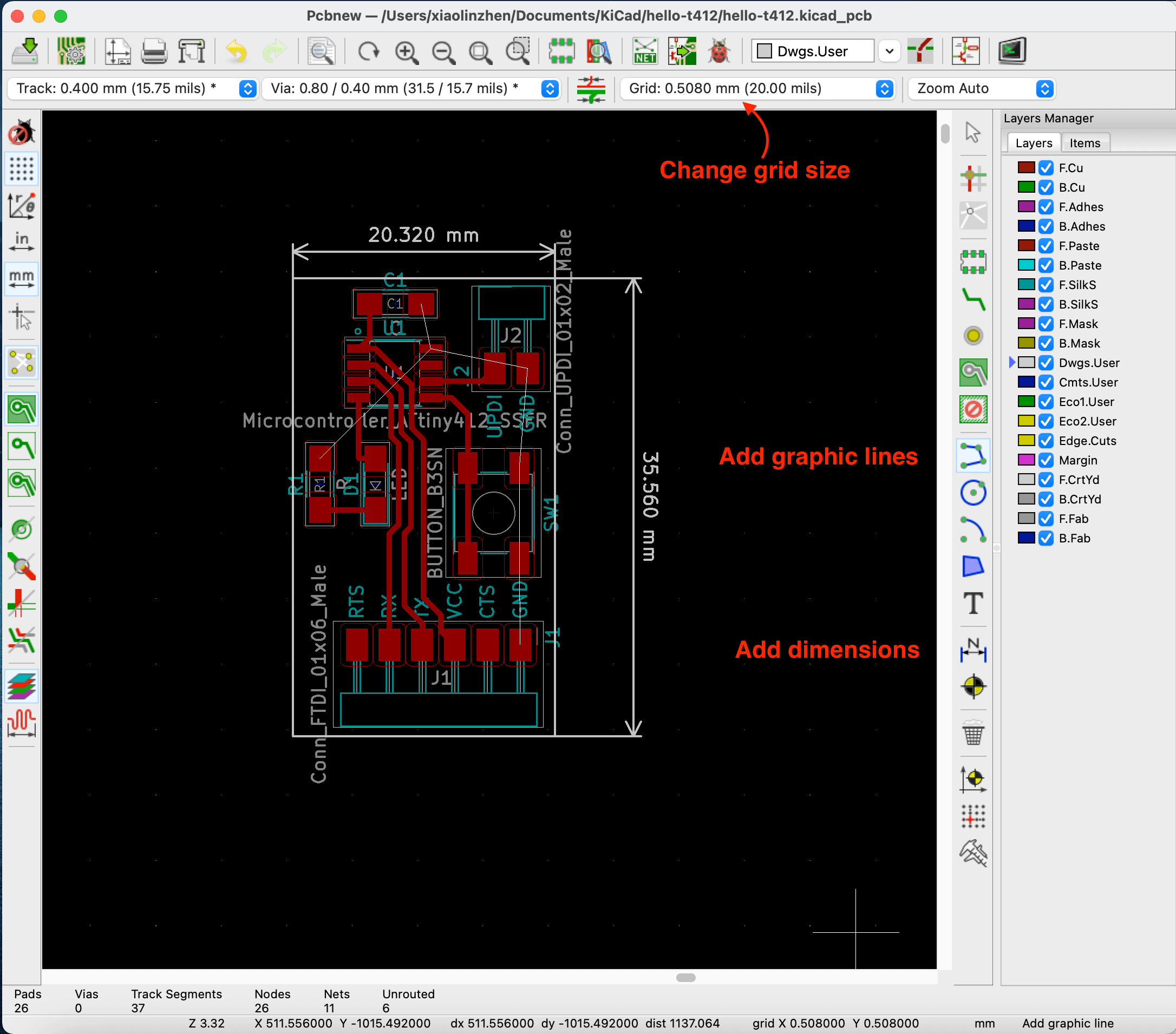
The layers were displayed on the right panel and these layers detated the industrial PCB making process, for example, F.Cu = Front Copper; B.Cu = Back Copper, Adhesive Layers, Paste Layers (for solder paste if using reflow technique), Mask Layers, Silk Screens, Drawing User, Edge Cuts...etc. Kris told us that, as we were only using single-sided FR1 board, we only needed F.Cu (for traces), Dwgs.User (for outline), and Margin (for outline offset) in our PCB designs.
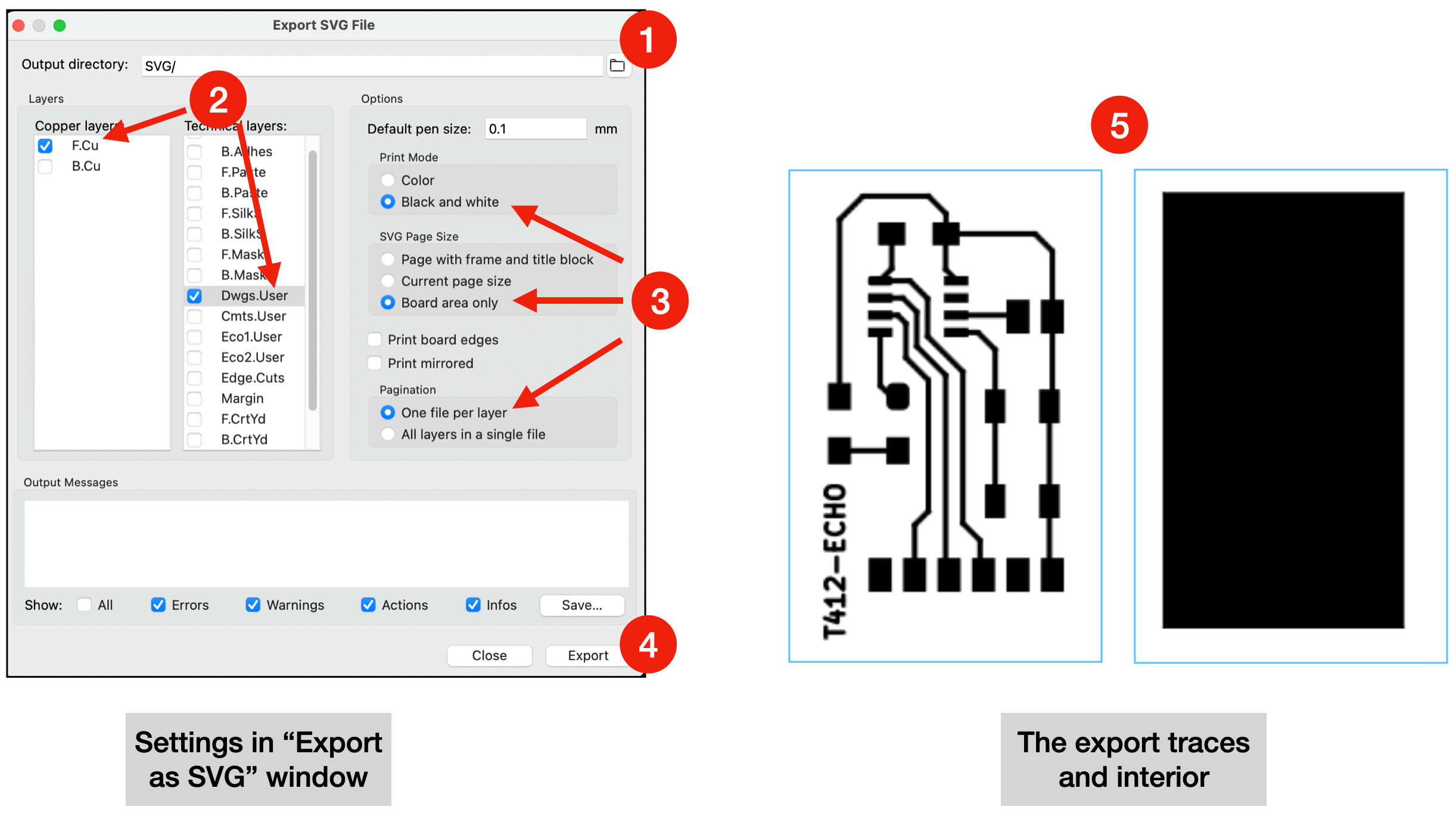
White area is what we want the machine to keep; Black area is what we want the machine to cut.
Milling and Soldering
I have went to the lab to mill and solder my hello.t412.echo board on Monday (9:30 am). Before doing that, I double checked my board and realized my TX and RX connections were different from Neil's board. In order to rectify this issue, I decided to re-route my board to allow for a smooth programming process later on. Yet, it was very slow going because the VCC (power), RX (receiving), and TX (transmitting) were always in the way of each other.
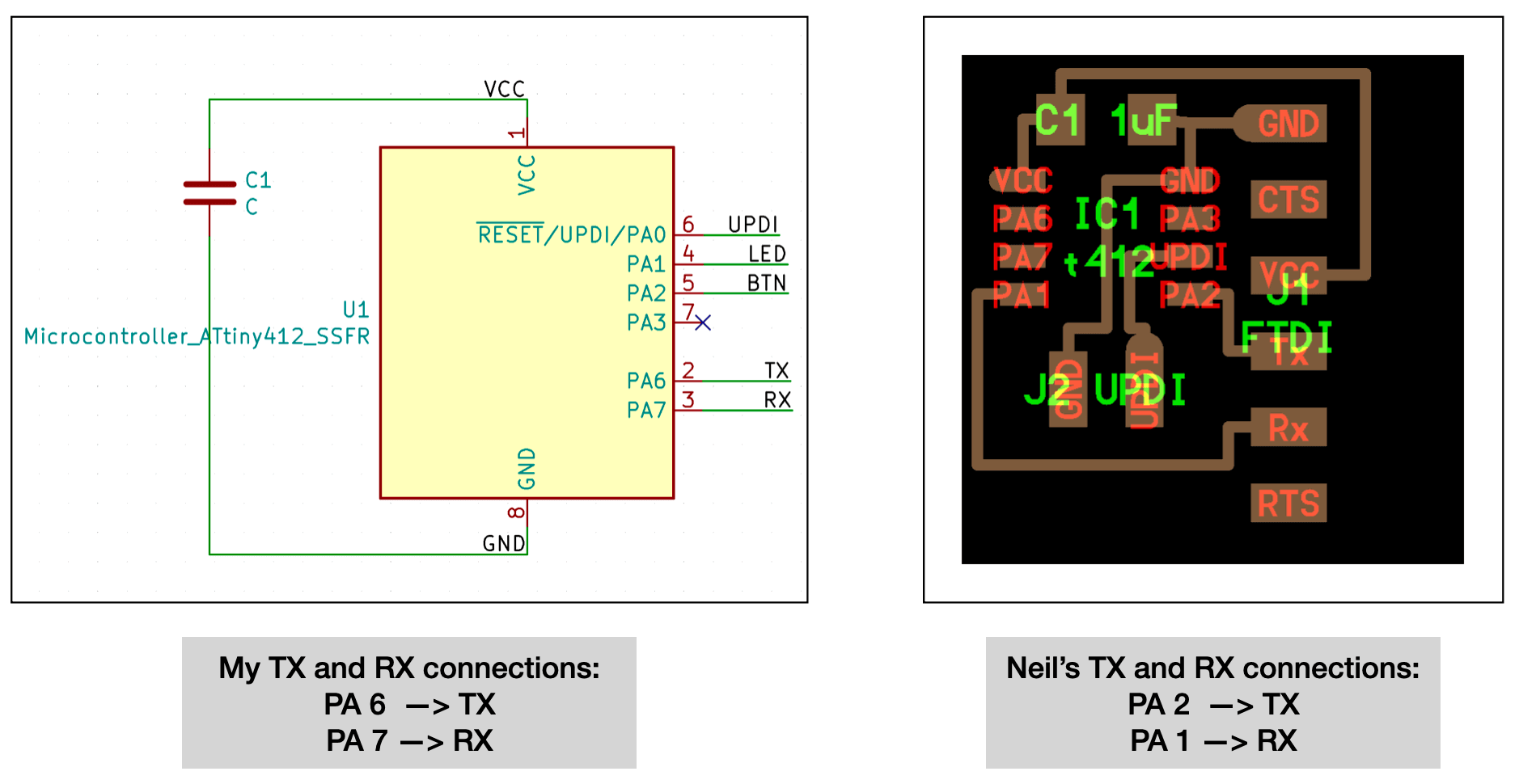
Then, during our weekly office hour (11:00 am), my classmate Nick told me that the connection on my original board was actually fine, because I was following the layout of the megaTinyCore image. He also shared to us a simple solution to make the Arduino code work without having to re-route the board 👍! (more on programming in my Arduino section)
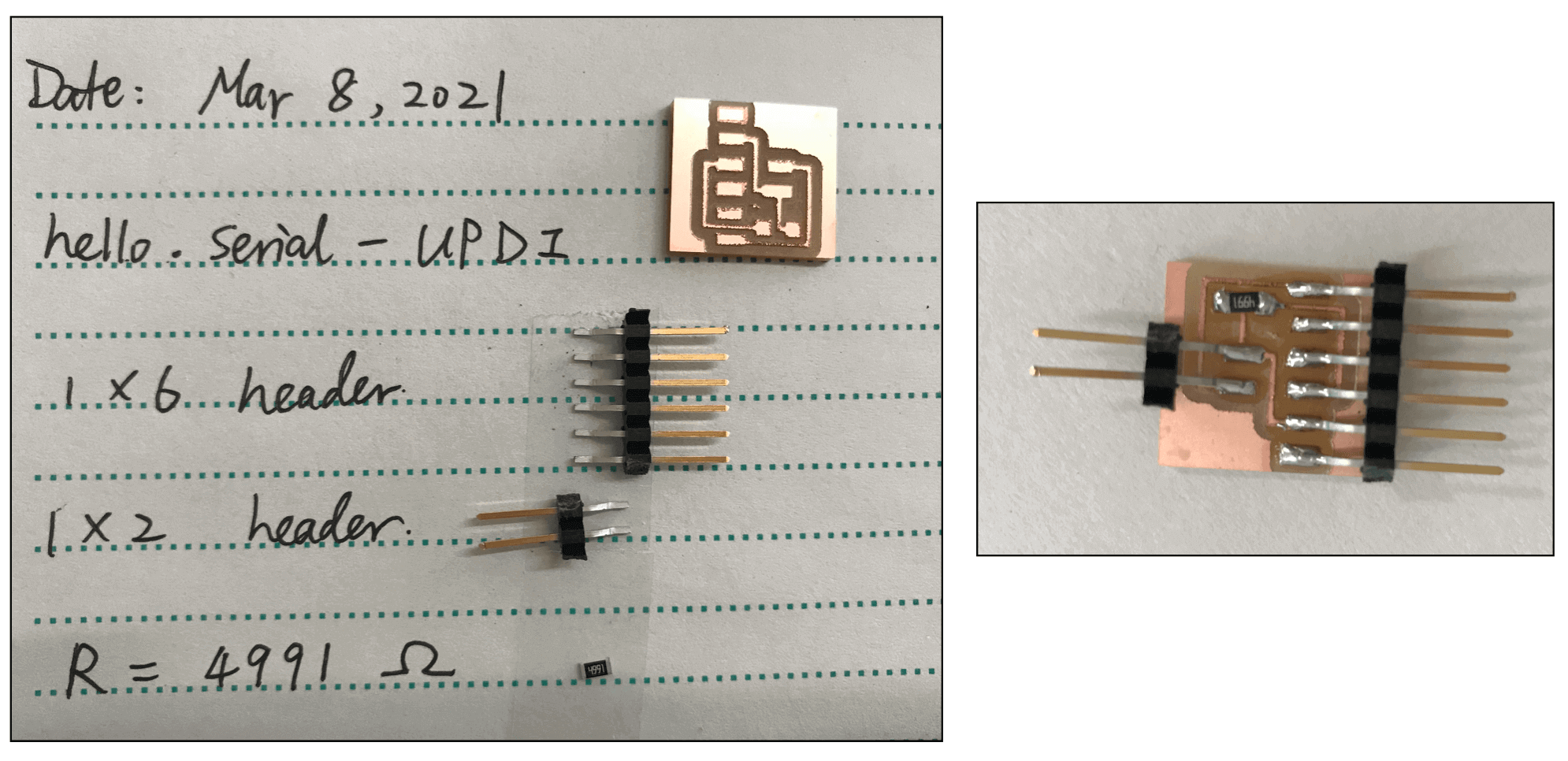
After I knew that I could use my original design, I proceeded to mill my hello.t412.echo board using the .rml codes that I generated the night before. I planned to use a red LED on my board so I did a quick calculation on what resistor I needed. The ATtiny412 data sheet pointed out that it would run from 1.8V - 5.5V, and for Fab Academy, we could use 3.3V or 5V on our boards. According to the website for the red LED, the Current - Test was 10mA, and the Voltage - Forward (Vf) was 1.8V, so using Ohm's Law, the resistor that I needed would be equal to the voltage drop / current, which would be 150Ω for 3.3 V and 320Ω for 5V. I decided to go for the 320Ω resistor because I wanted to make my LED work at any voltage, and I ended up using a 499Ω resistor because that was the only type within 100Ω and 1KΩ at the lab.
R = (3.3V - 1.8V) / 0.01A = 150Ω
R = (5V - 1.8V) / 0.01A = 320Ω
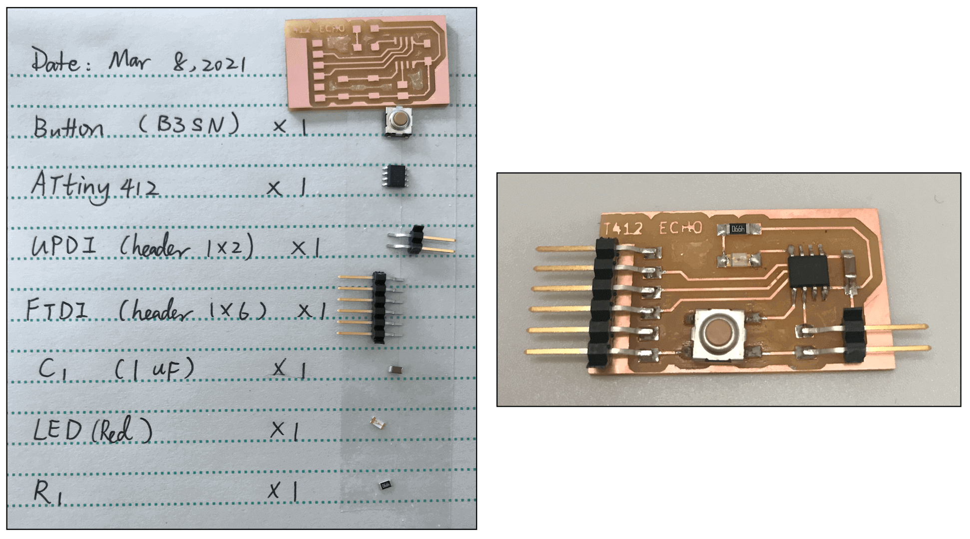
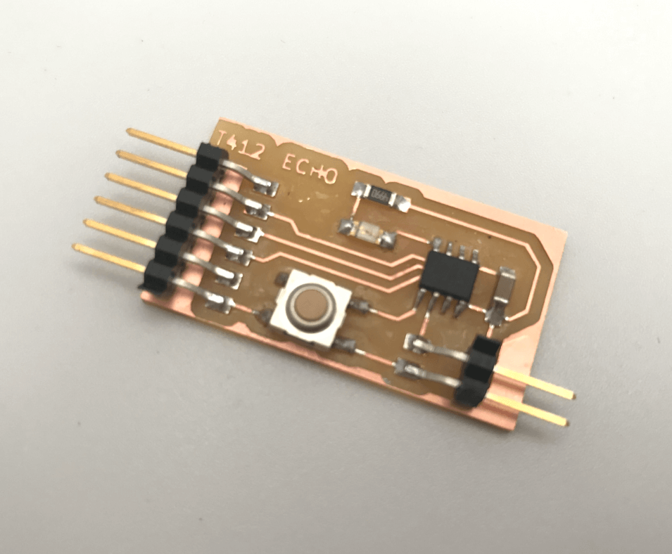
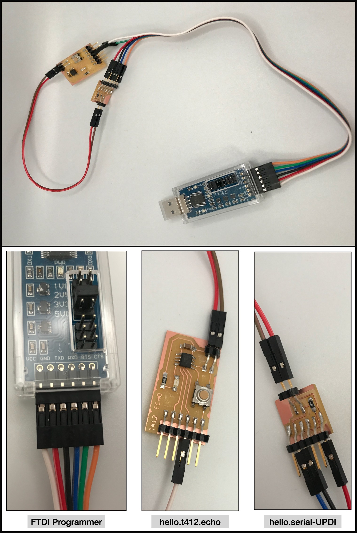
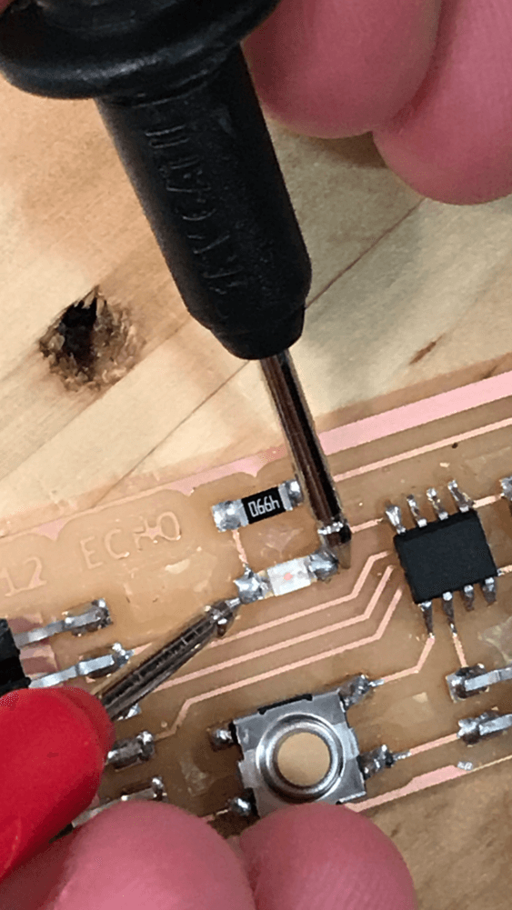
For this assignment, I planned to use the FTDI programmer from my class kit since my SAMD11C14 programmer was not ready yet. To get ready for programming, I also milled and soldered a hello.serial-UPDI board as suggested by my instructor Spencer and my classmate Nick. The milling and soldering went great, I was aware of the polarity of the IC and LED components so there was no problem there. However, my board didn't pass the continuity test the first time and I wondered if it was because of the orientation for my button, so I checked with my instructor Spencer and he confirmed that I had turned my button by 90° counter-clockwise 😅 (or -90°). After desoldering the component and making the correction, I ran a continuity test again and it passed this time. (more on continuity test in my Multimeter section)
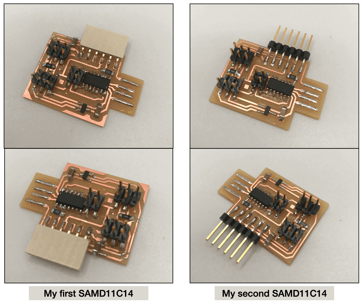
In addition to milling and soldering these two boards, I also finished soldering my second SAMD11C14 because the one that I did on Week 4 didn't pass the continuity test due to broken copper traces in multiple places. This time, I learned to be patient and heated my solder for a little longer before letting go of the soldering tip. I was pleasantly surprised by the result of this trick and also my improvements within these two weeks. That night, I showed my work to my family, and my dad was so proud that he had to take portraits of my boards using his phone 😆.
Assignment 2: Testing the Board
Using Test Equipments
Multimeter
We have a multimeter in our class kit. It is an electrical testing equipment that is designed to help measure alternating current (AC), direct current (DC), voltage, and resistance. Some advanced multimeters can help measure capcitance and indutance. I found this SparkFun YouTube video very helpful for getting me to understand the basic concepts of a multimeter and its usages.

A couple weeks ago, our instructor Greg gave us a lesson on how to do a continuity test on our PCBs using a multimeter. In general, we performed a contunity test to check our electronic connections, or the complete path for current flow. Specifically, we would first check for the GND connections, then the VCC connections, then VDD...etc. The multimeter would beep if a complete path was detected. However, we also wanted to use the continuity test to check for fuses. If we heard the beep in a spot that it was not supposed to be at, then we knew there was a fuse and we need to solve it before using it practically. Here is a short video of me testing the continuity of my hello.t412.echo board.
Using Arduino
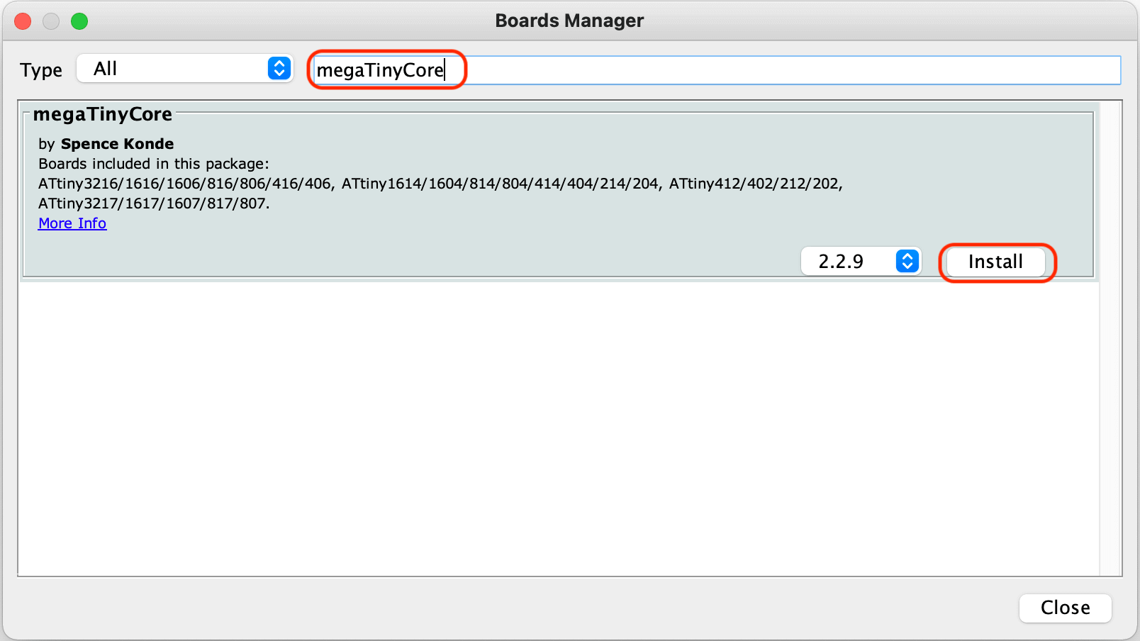
To begin, I installed Arduino 1.8.14 on my computer, I then installed the megaTinyCore via the Arduino Board Manager by following this installation instruction. After confirming that ATtiny412 was on my Board list, I then proceeded to the next step.
I followed my classmate Nick's set up to make connection of the FTDI programmer with the hello.serial-UPDI board and the hello.t412.echo board:
- FTDI -> UPDI (hello.serial-UPDI): connect the GND, RX, and TX
- UPDI -> echo board (hello.t412.echo): connect the GND and UPDI
- FTDI -> echo board: connect the VCC (used 5V mode on FTDI)
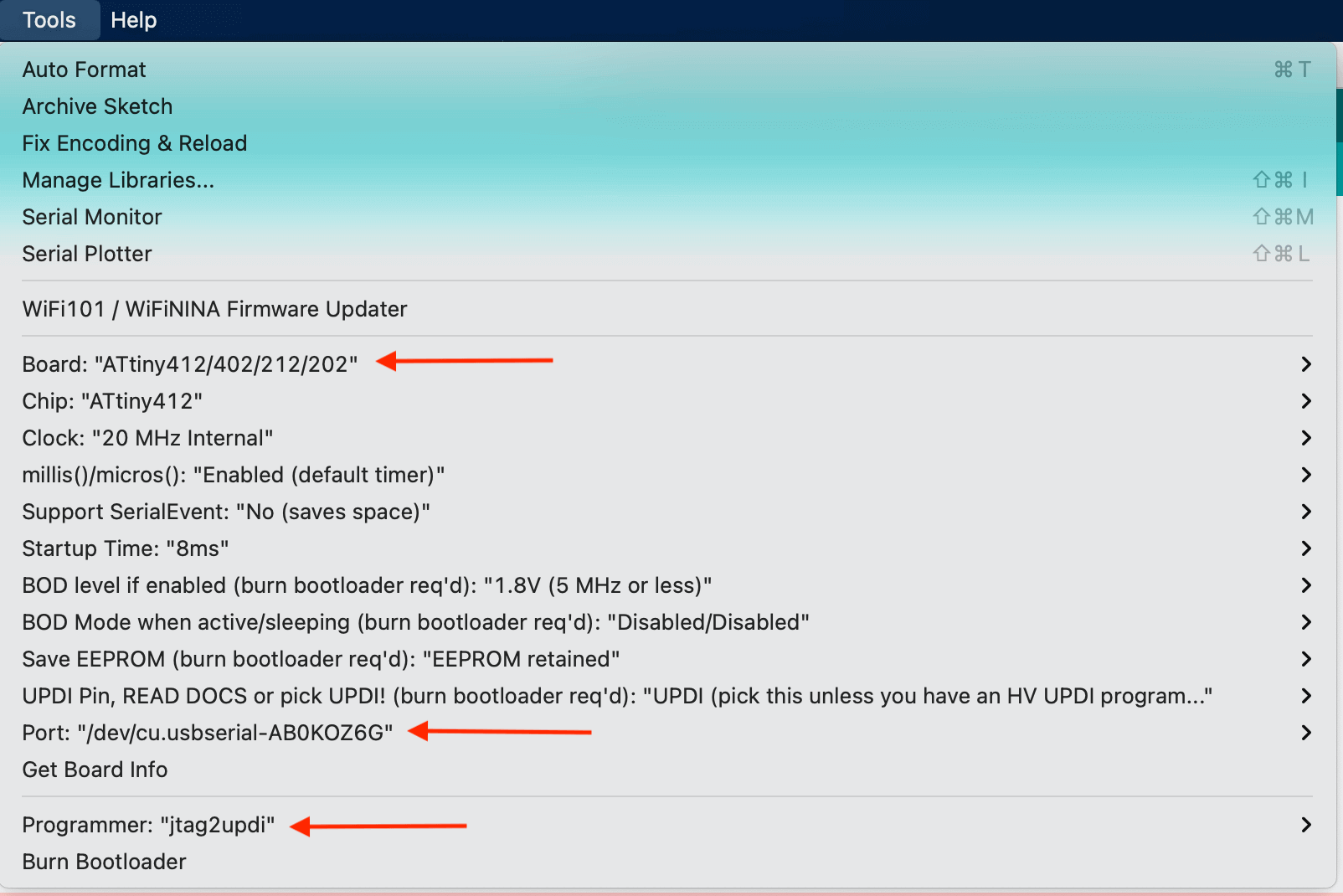
Then, I plugged my FTDI to the USB hub of my computer, I also made sure to select the correct Board, Port and Programmer.
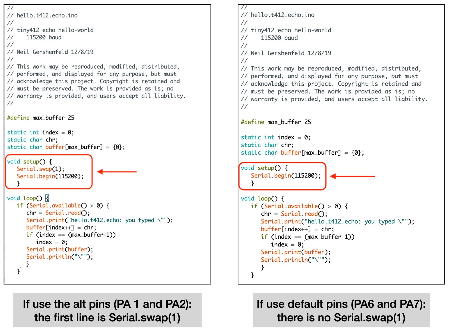
After that, I downloaded Neil's hello.t412.echo.ino and opened it in Arduino IDE. As mentioned previously, my connection on the TX and RX were different from Neil's, and I did not have to re-route my board because I could make a simple change in the Arduino code instead 😃. According to the ATtiny412 datasheet, when the first line in the code was Serial.swap(1), it was asking for the alternative pins. Since I was using the default pins to make my connections, all I needed to do was to remove the Serial.swap(1) line from Neil's code.
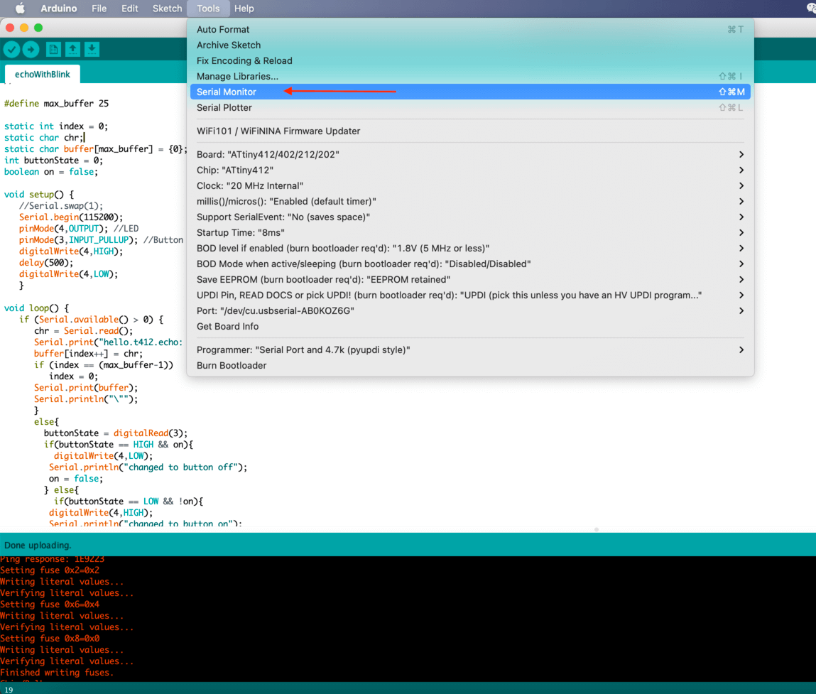
Then, I clicked Upload but I received an error as shown below:
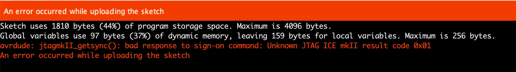
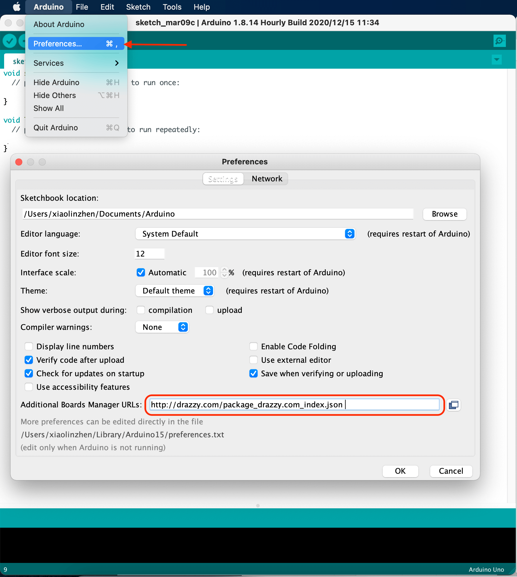
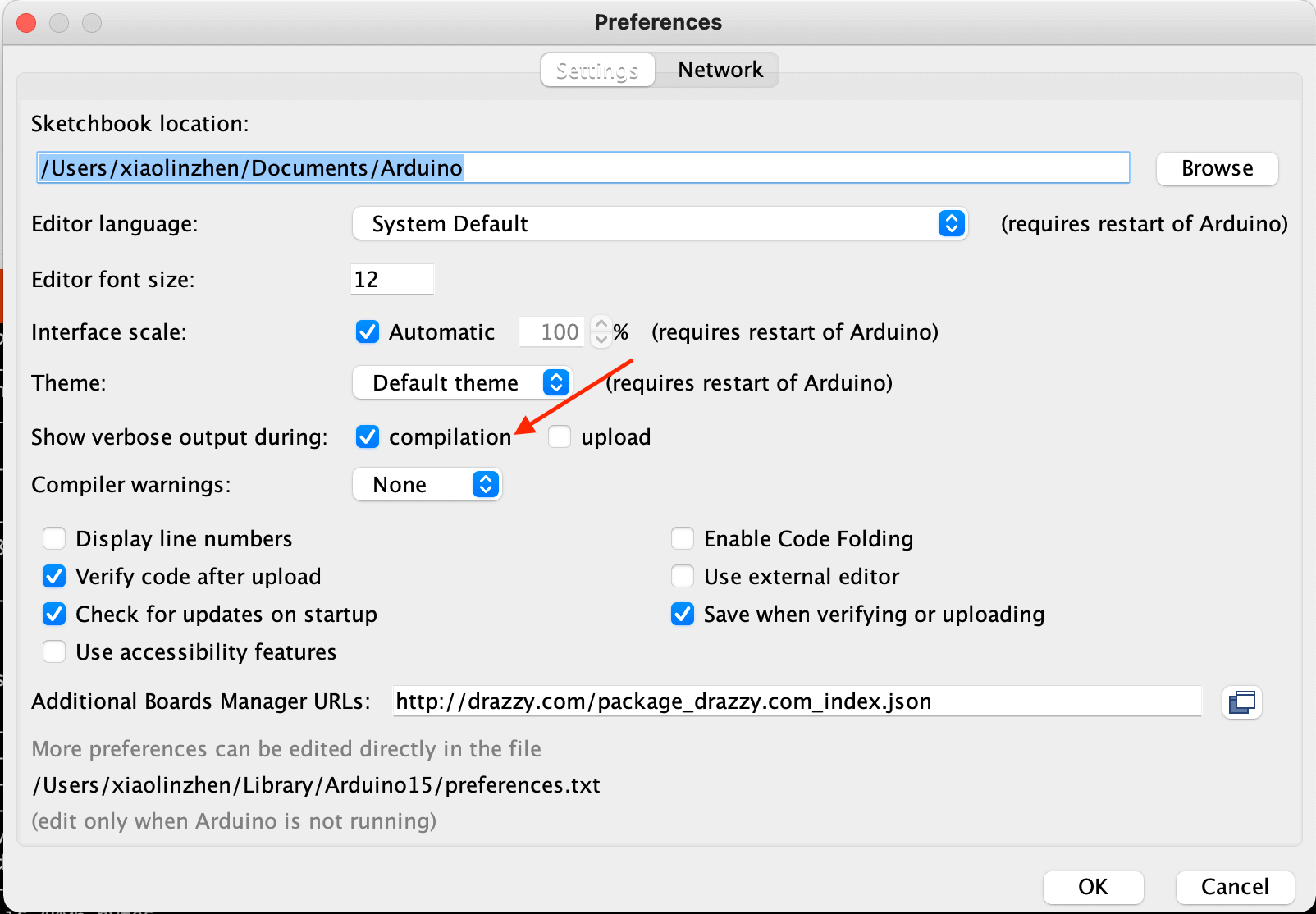
I copied the error messages attempting to find out the reason, and I was instructed by this message: "This report would have more information with "Show verbose output during compilation" option enabled in File -> Preferences". So I enabled the option (image 1) and checked to make sure my connections were correct, then uploaded the code again. This time, I was greeted with a more detailed error message as shown in image 2...
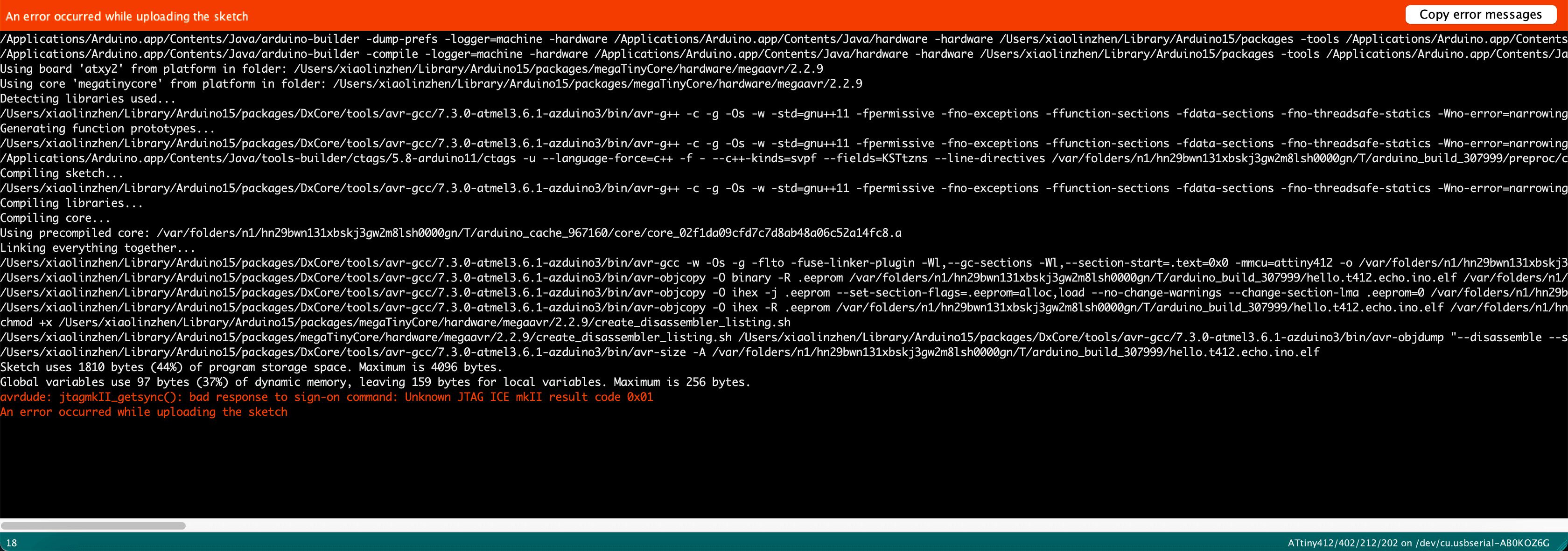
I examined the message but I couldn't find a clue, so I googled this error message to look for a resolution. Yet, the only place that pointed out to something similar was from this thread.
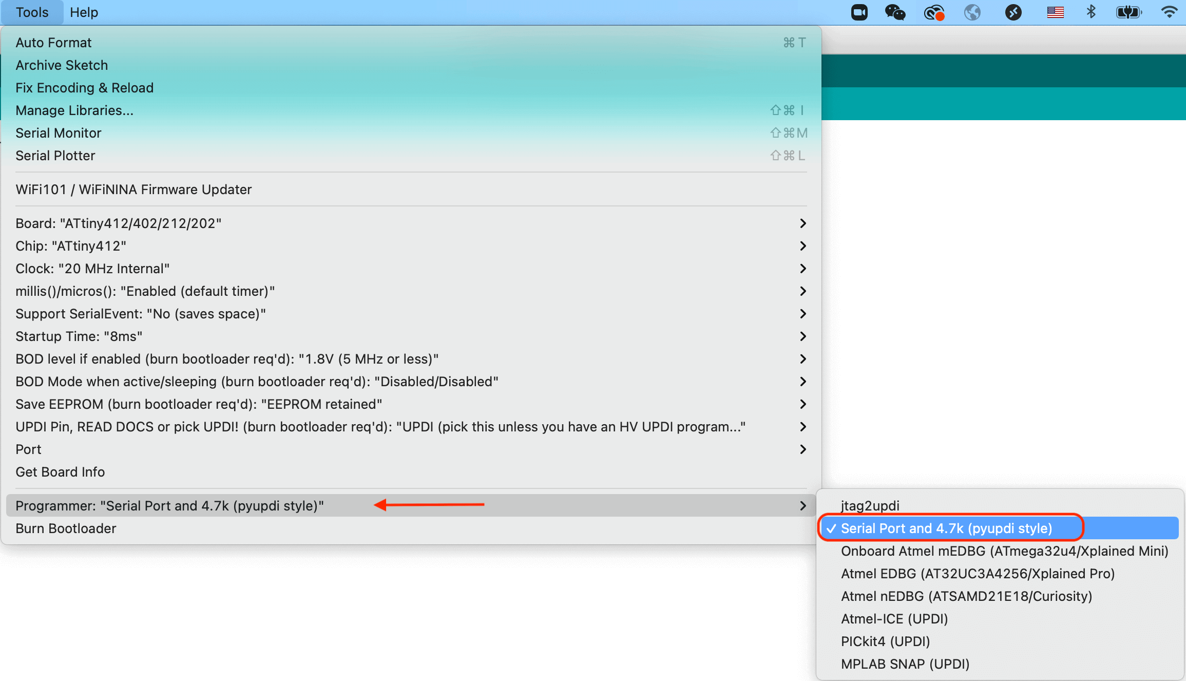
Mar 10, 2021I restarted my computer and also reinstalled Arduino and megaTinyCore, however when I uploaded the program, I still received the same above error, so I posted the error message that I received on my class Group Chat, and was informed by Nick that I actually picked the wrong Programmer. The correct Programmer should be Serial Port and 4.7k (pyupdi style).
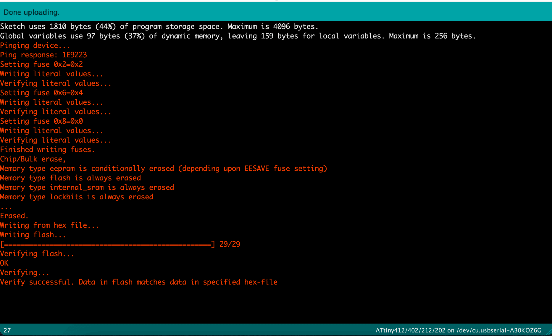
After changing the Programmer and making sure the connections were correct, I uploaded the code again. This time it was successful!
Mar 11, 2021
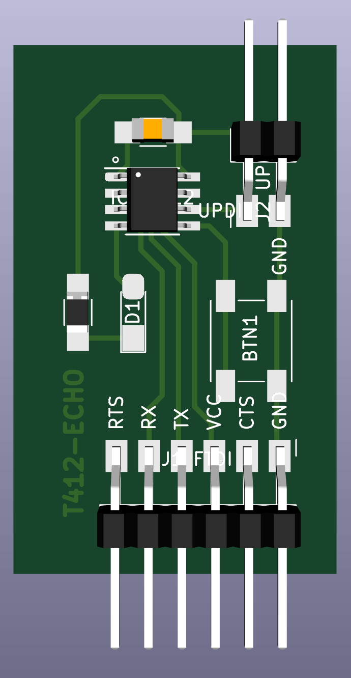
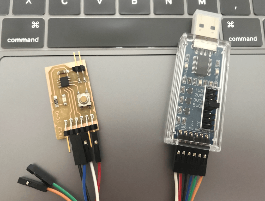
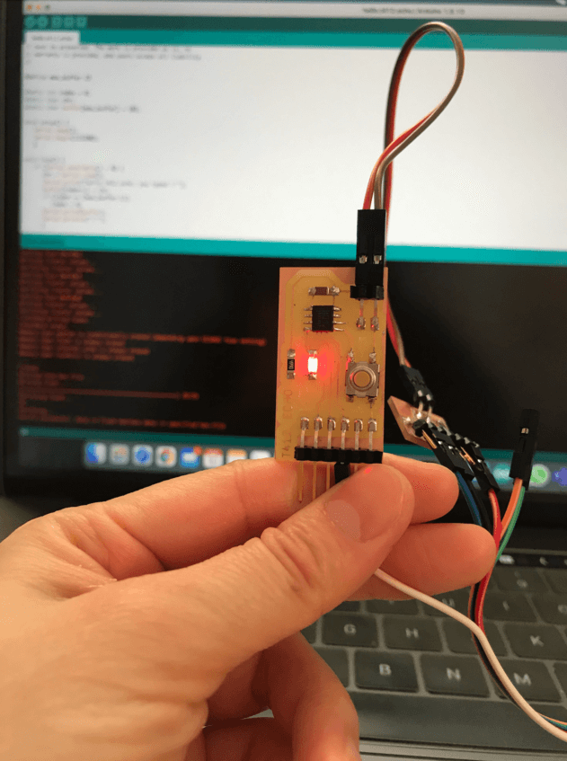
With the Programmer issue being fixed, I was ready to test the echo hello-world code and the blink code. In this exercise, we have used Nick's echo-with-blink code as our starting point. First, I needed to remove the UPDI adapter from the FTDI Programmer, and connected the FTDI directly to my board as shown below, once again, I opened up the 3D View of my board for reference. The TX and RX wires needed to be set up like this so that they could be communicating to each other (transmitting and receiving information).
- FTDI GND (red wire)--> echo board GND
- FTDI VCC (white wire)--> echo board VCC
- FTDI TX (black wire) --> echo board RX
- FTDI RX (blue wire) --> echo board TX
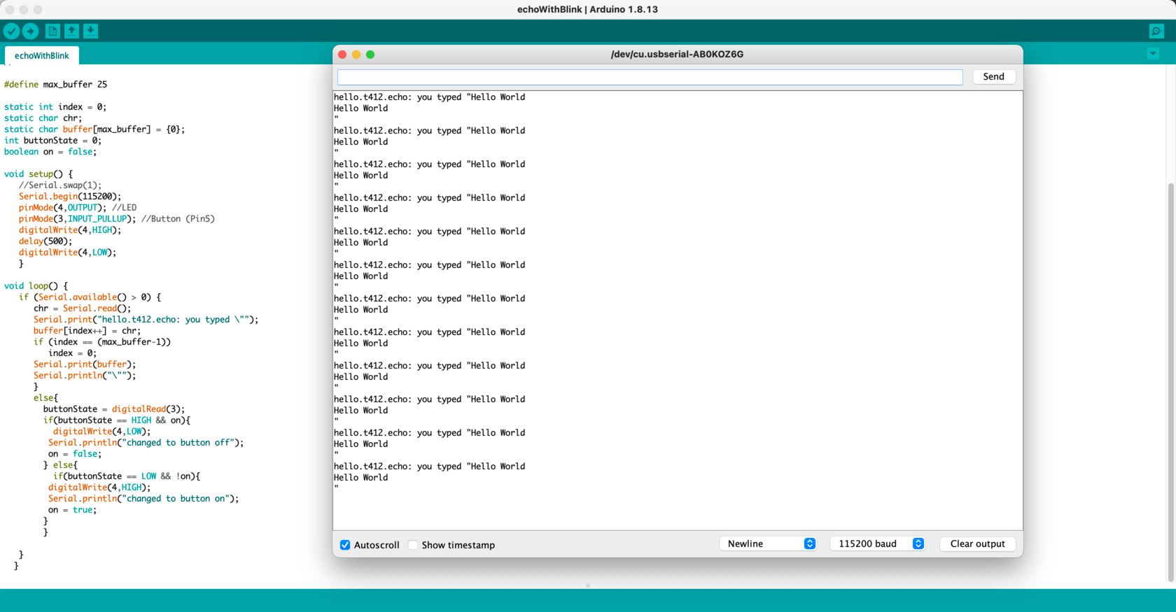
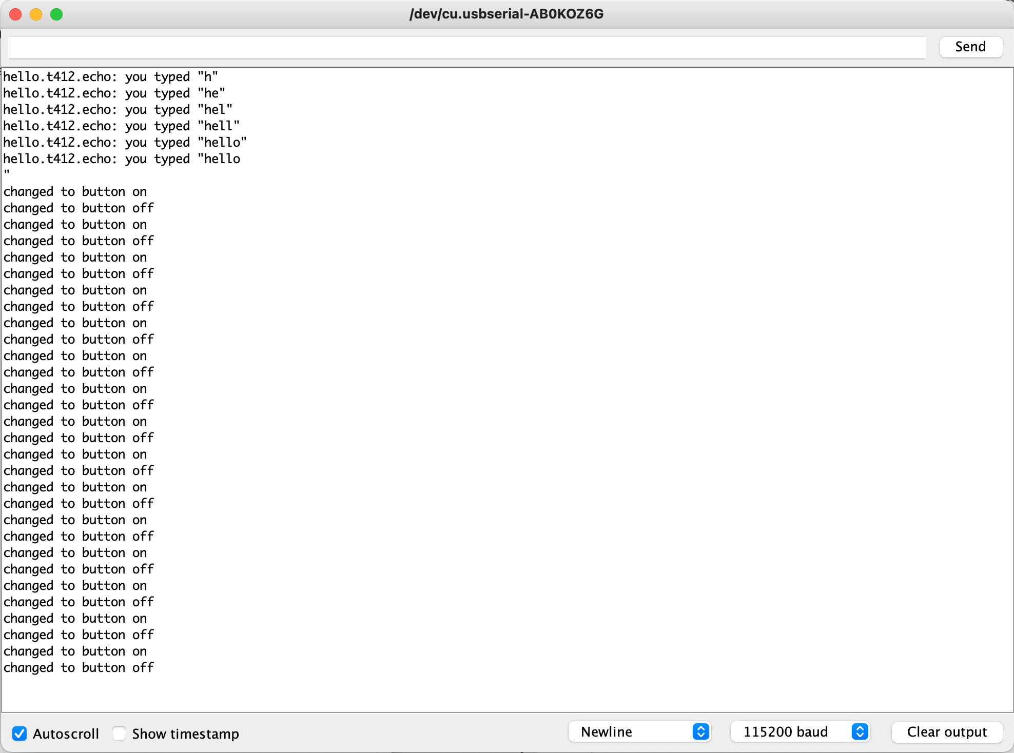
I opened the Serial Monitor and typed "Hello World", then hit "Send". In a second, the board echoed back the text that I typed.
I also tested my button, and found that it was working.
However, I couldn't get my LED lighted up. I have confirmed that the LED was oriented correctly, but there was only a tiny bit of red shown up when my classmate Griffin helped test it with a multimeter. After back home, I tested my board on the Arduino "Blink" example, yet I still couldn't get the LED to light up, so something must be wrong with my LED.
I recalled that I have tested my board on a hello-echo code designed for ATtiny1614 instead of the ATtiny412 yesterday. At that time, my LED was bright red as soon as the code was verified uploaded. However, that was the only time that I had seen it lighted up, probably I had broken my LED already and there was no way to resuscitate it 😔. To remedy my current situation, I would need to replace my LED and test again. (to be continued...)
Mar 19, 2021
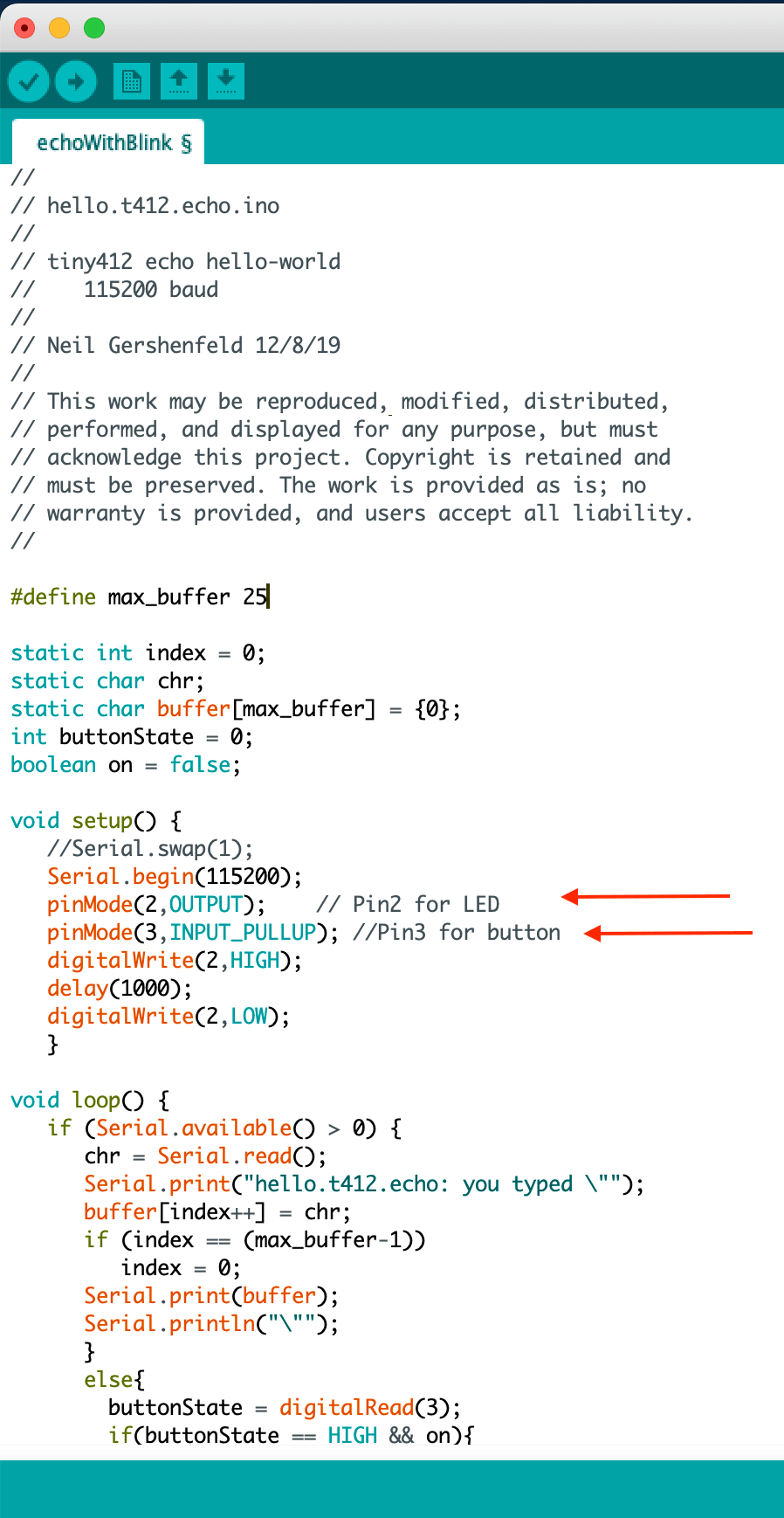
I realized that I have input the wrong pin number for the LED, so I didn't break my LED 😊. After fixing my error, I tested my board on Nick's echo-with-blink code again, this time it blinked!
Here are the snapshots of the code and the results.
Here is a short video for the hello-echo-blink Arduino sketch.
Files
Please find below the files that I made for this assignment.
- The hello.t412.echo Board
- KiCad files
- SVG files (Traces + Interior)
- RML (G-code) files (Traces + Interior)
- Arduino file