
This work is licensed under a Creative Commons Attribution-NonCommercial-ShareAlike 4.0 International License
Activity Log 2: Electronics Design and Production
Summary
During Week 8, Week 11 and Week 13, I have aquired skills such as interpretting datasheet of different chips, setting up my input device (accelerometer/gyroscope) and my output device (vibration motor). In those weeks, I used tinyAVR-1 series as my processor. Later, during the Networking and Communications Week, I chose to upgrade my board with the ESP32-WROOM-32 as the processor, the main reason for that was because this microcontroller has the bluetooth feature, which would help with the bluetooth application development of my project.
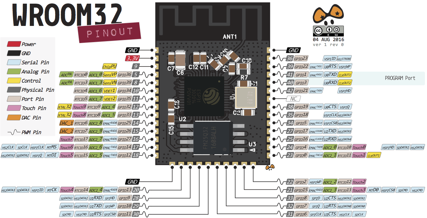
ESP32-WROOM-32
May 4, 2021Wroom32 pinout
PCB Design
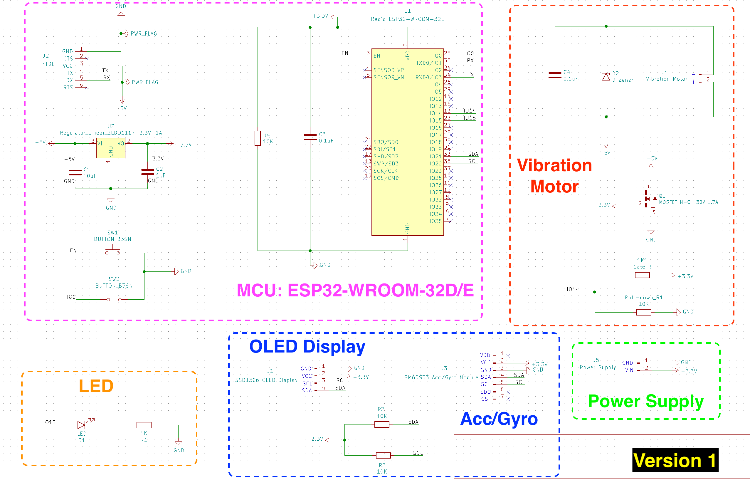
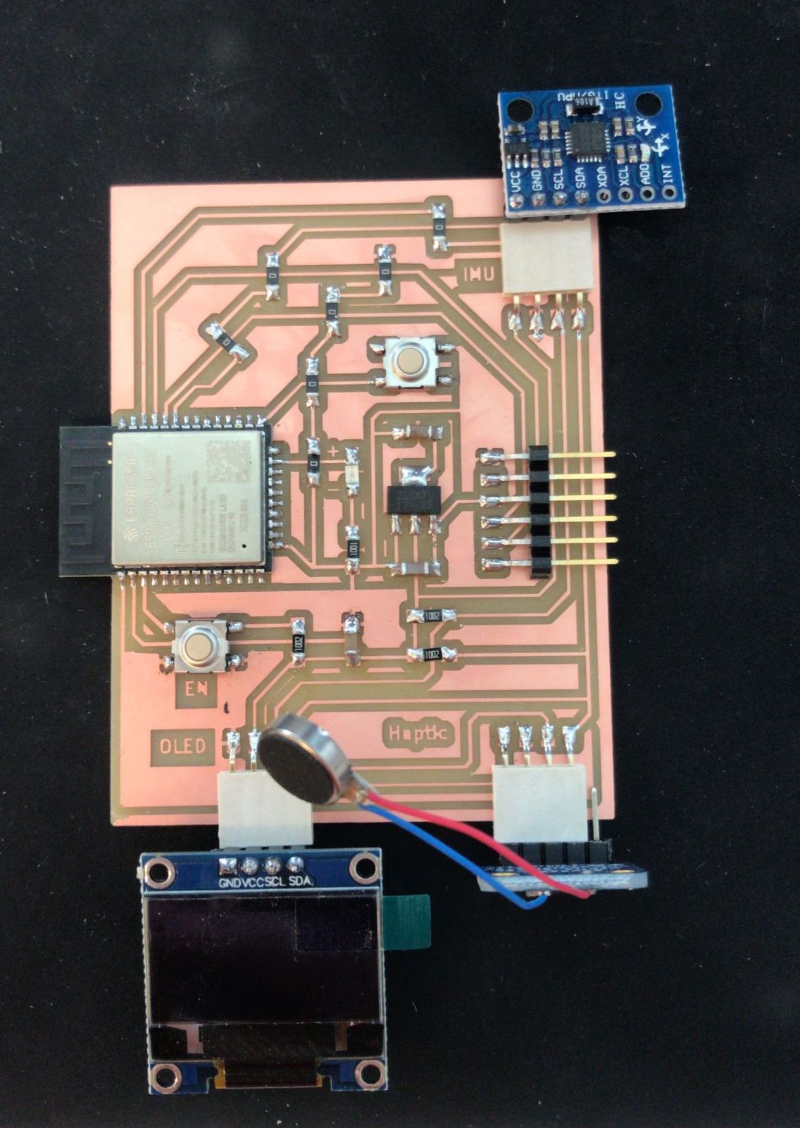
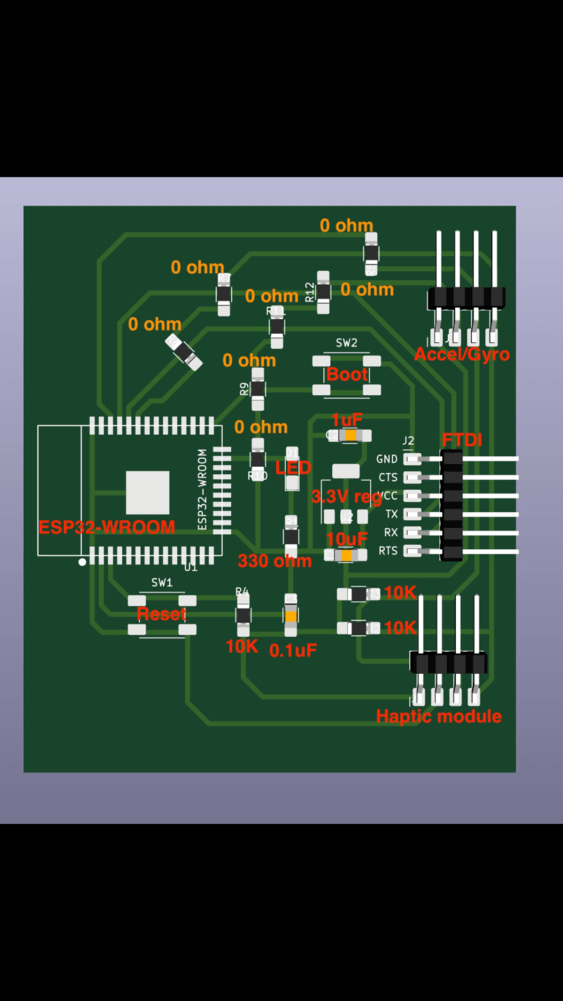
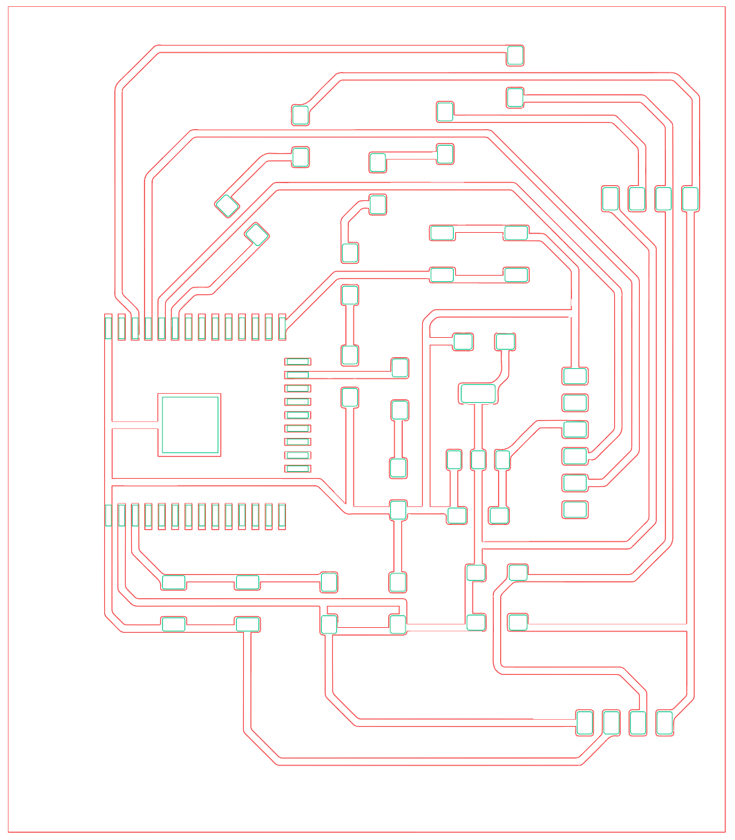
PCB design Version 1: inspired by Griffin's design, I put all my I/O devices into one board:
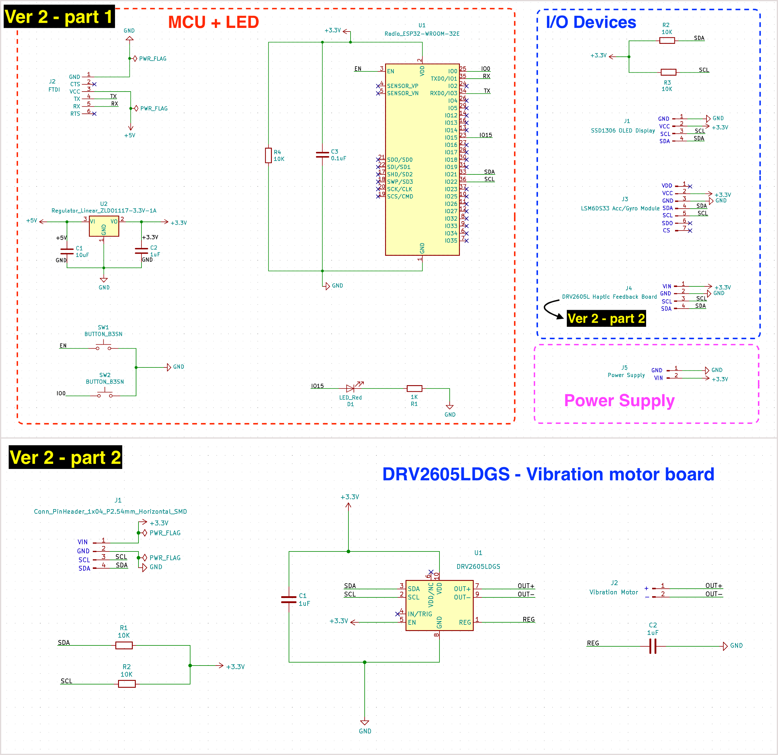
Version 2: notice that I replaced the vibration motor in version 1 with a "haptic feedback board", the one that I was planning to use was Adafruit's Haptic motor Controller as I could use the SDA and SCL pins for I2C communication. In the second image, I reproduced Adafruit's PCB design for this board using KiCad.
May 6, 2021
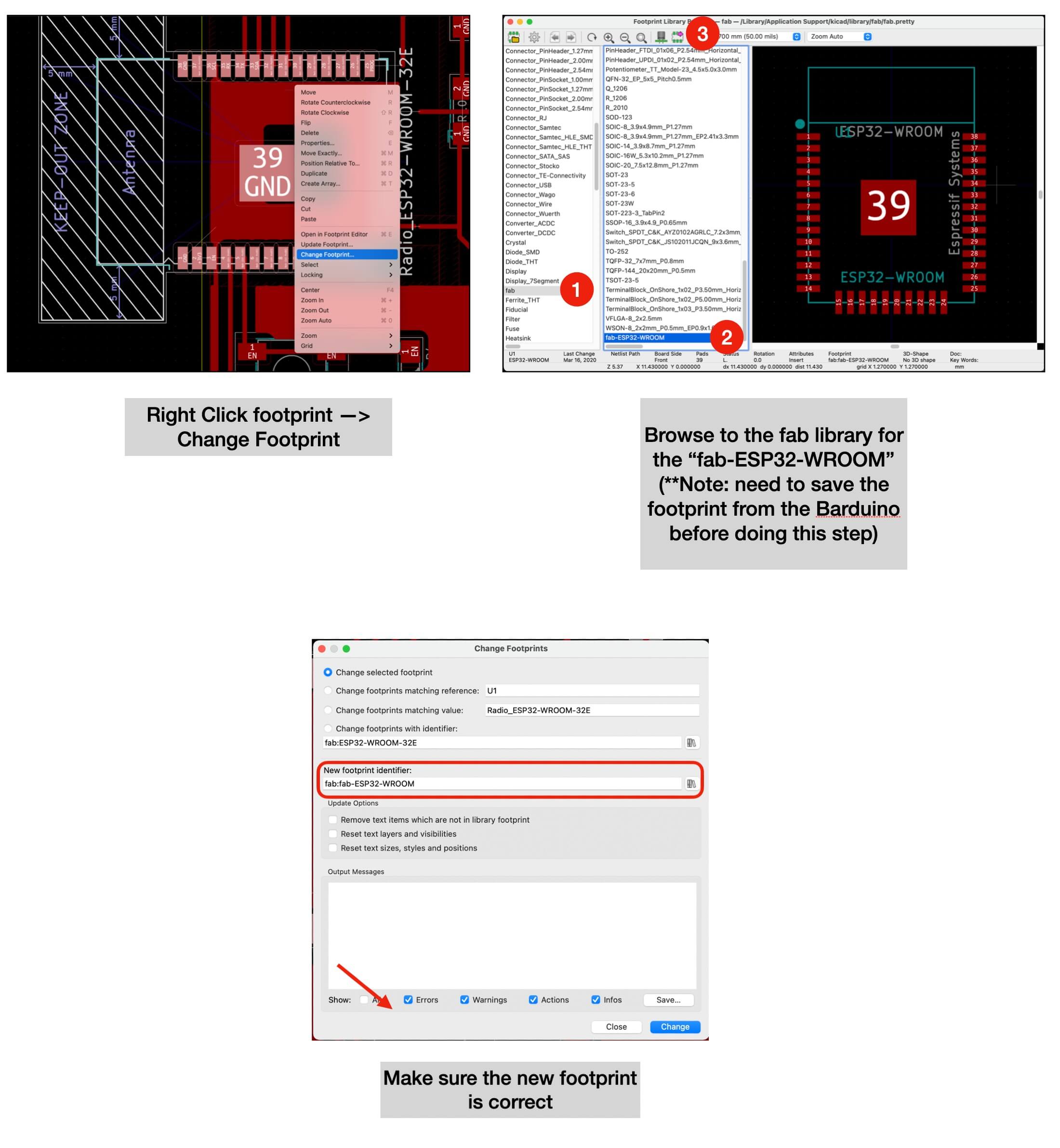
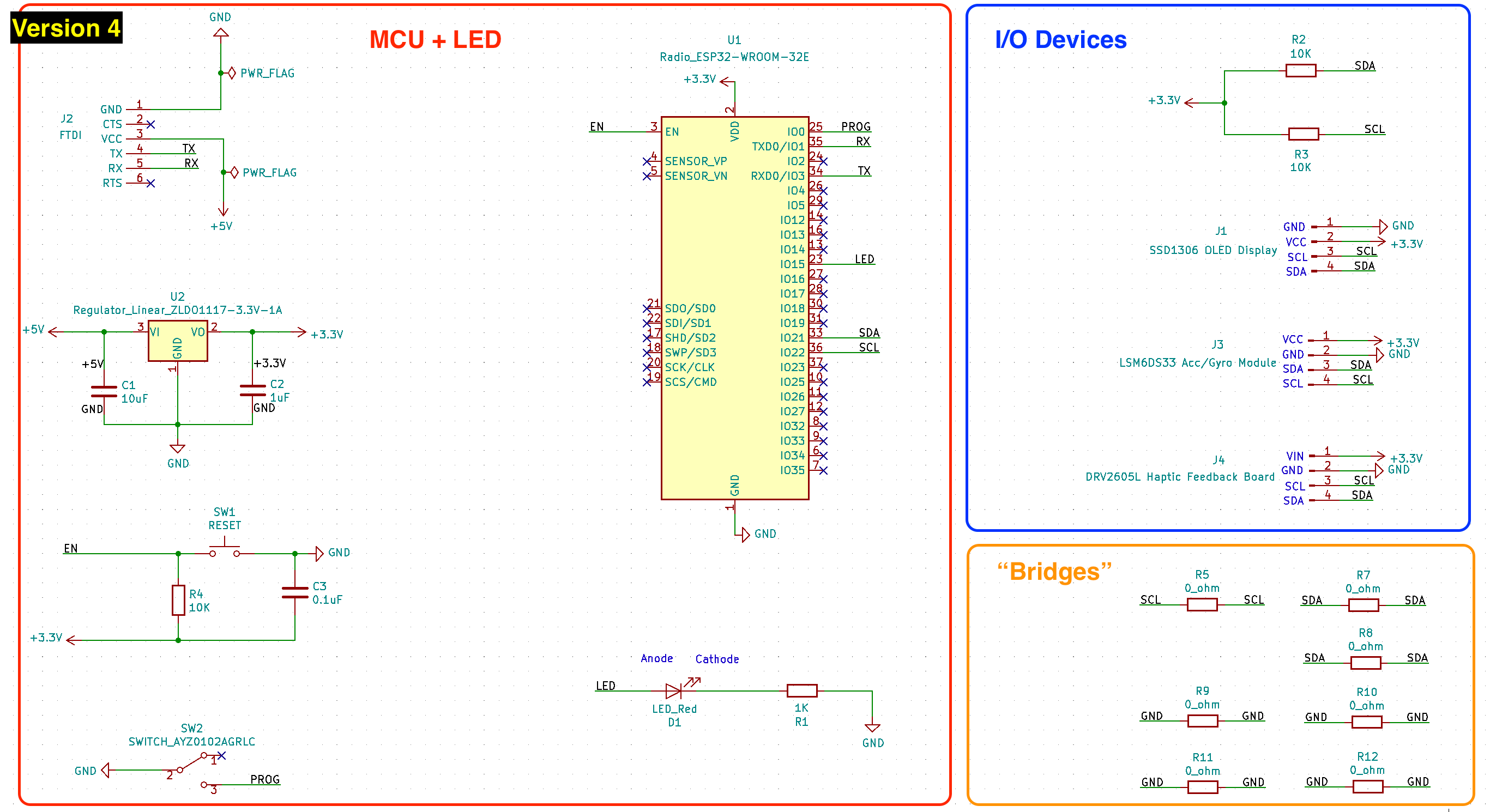
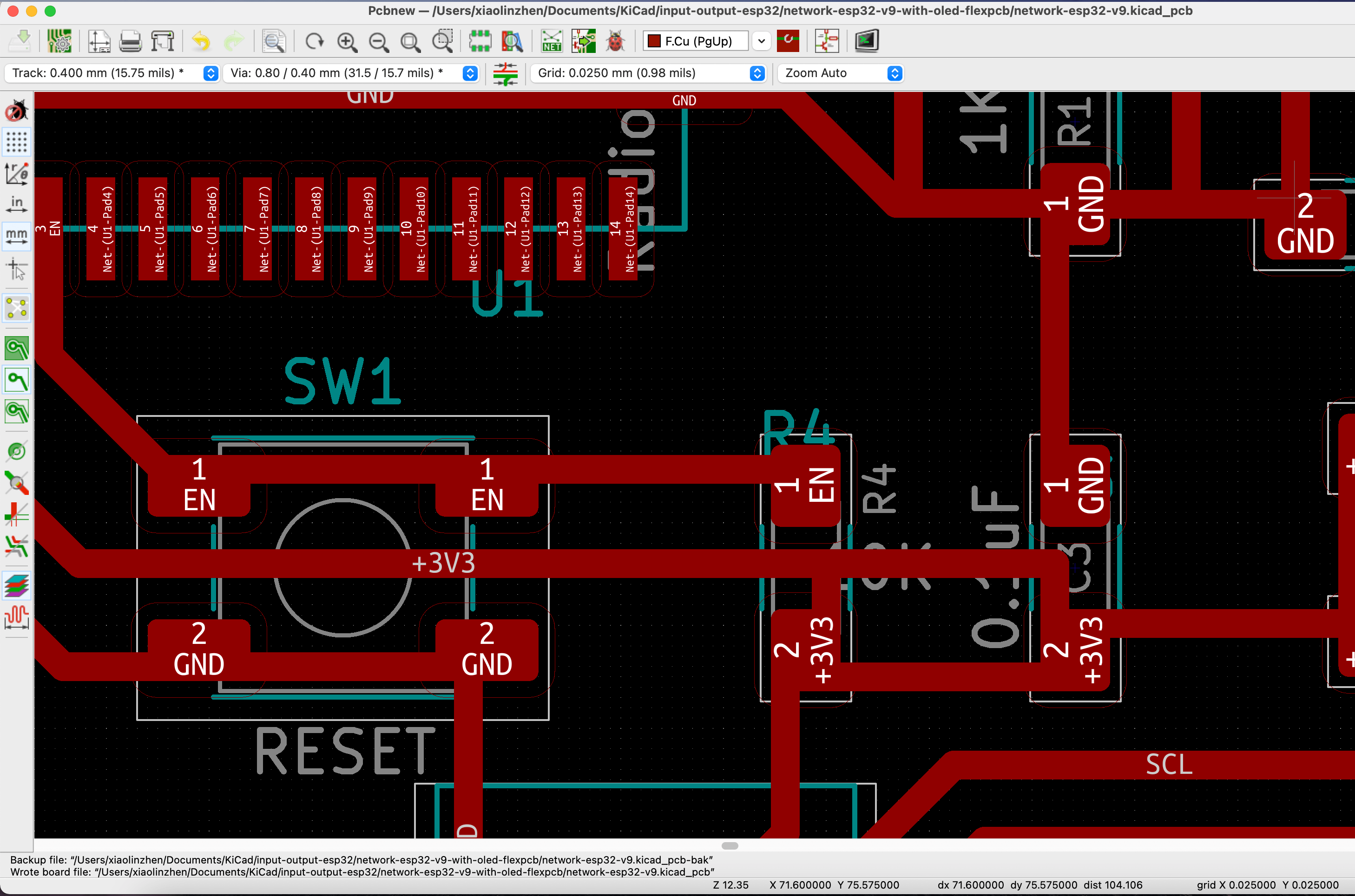
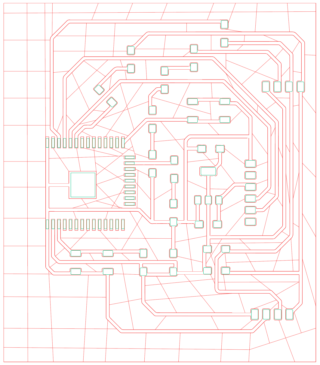
Version 3: 1) Fixed the schematic errors that I made and added eight 0 ohm resistors as the bridges; 2) removed the power supply since I was not sure if the battery alone would work for the system; 3) replaced the ESP32-WROOM footprint with the one in Barduino 2.2 in order to pass the electronics rules check.
Please note that this layout may only work for non-flex PCB production process, since the small pads may struggle staying on the sheets during the weeding process.
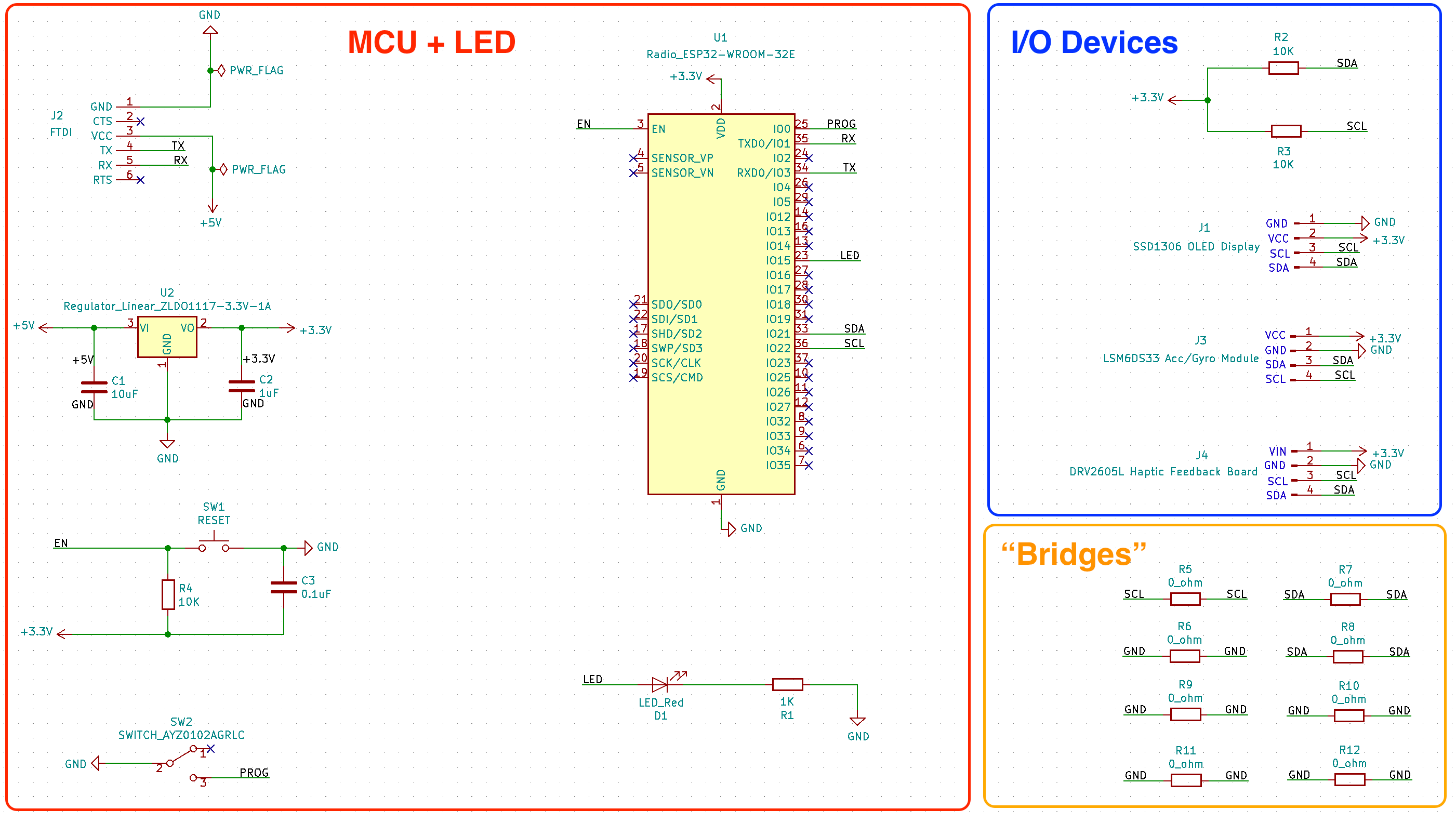
The white/blue components are from Neil's board and I tried to arrange the components in the same way as his board. The purple/black components are the extra ones for my board. The ones without labels are the 0 ohm resistors
May 7, 2021
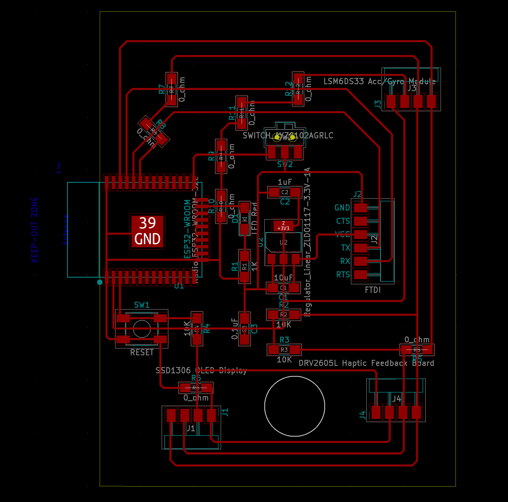
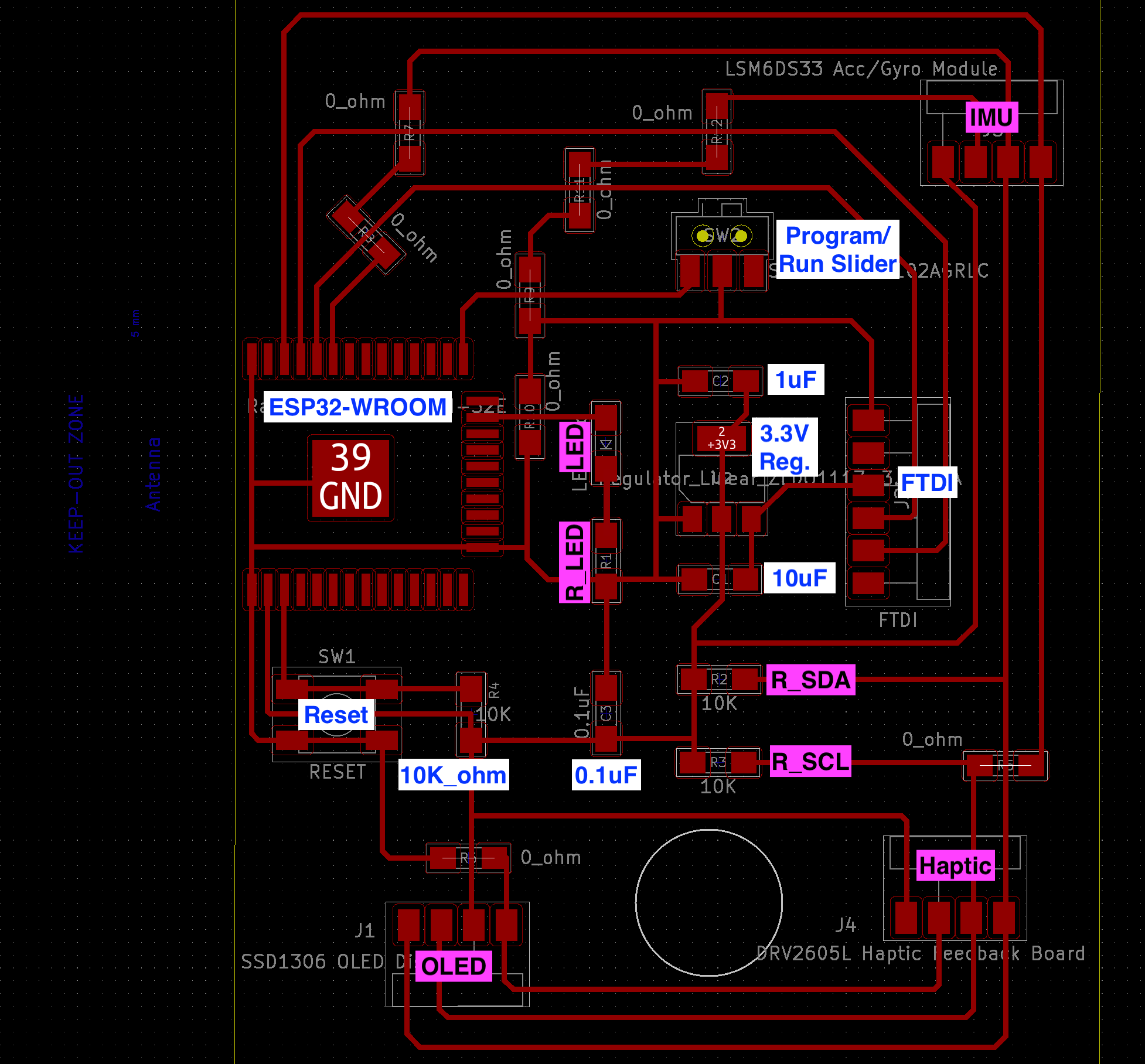
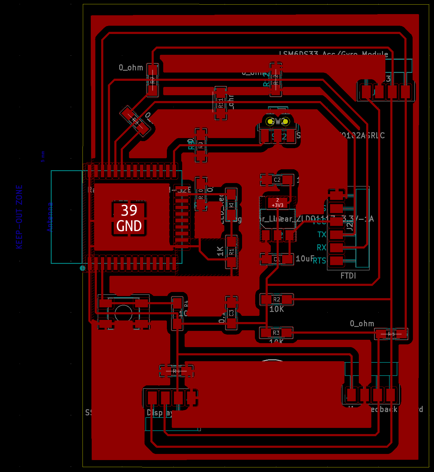
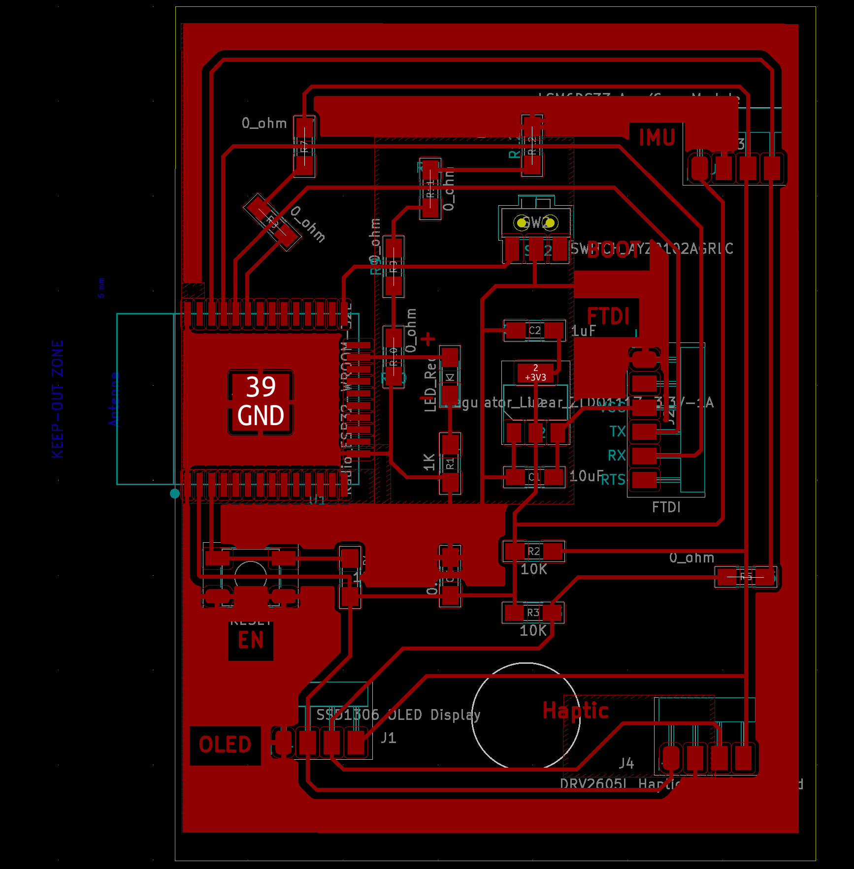
Since I knew that it would take a while to fabricate this board, I decided to spend time making sure my PCB design was correct. I used the built-in "caliper" in KiCad to measure the distances between components to make sure I had left enough room for every component - I found this approach helpful because I realized that I did make a mistake on the OLED display and the Haptic Feedback board. I was able to solve this issue by rotating the OLED board, and also bringing the Haptic Feedback board further away from the resistor. As a result, I was also able to use one fewer 0 ohm resistor. When doing the "ground pour", I blocked out a big area between the FTDI and the ESP32 in order to avoid the FTDI connect directly to the ESP32 without passing the capacitor, since I placed multiple 0 ohm resistor in between. Here are the updated images for the PCB design:
PCB Production on FR1 Boards
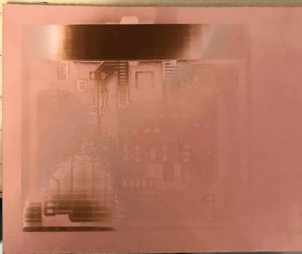
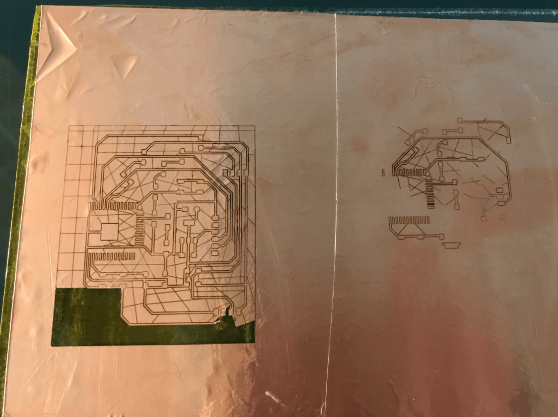
May 10, 2021Part 1 - Laser cutting attempt
Part 2 - Milling and Soldering
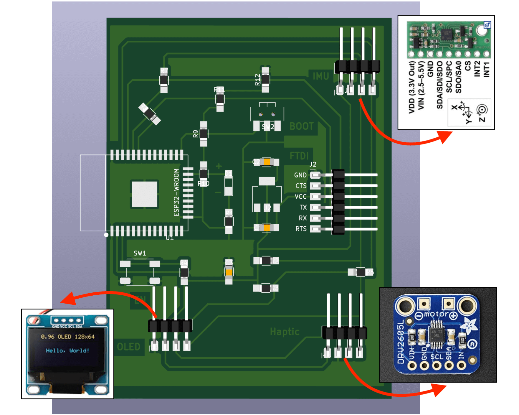
I/O Devices Testing on the FR1 Prototype
1) Test the Accelerometer/Gyroscope module and OLED display
2) Test the Haptic Controller module
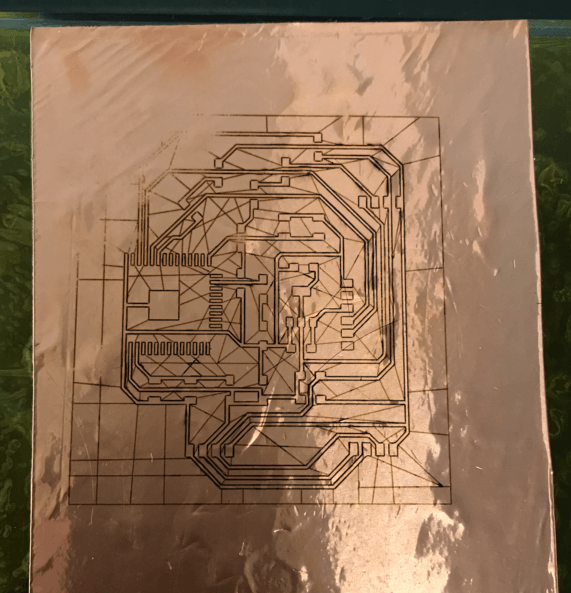
Flexible PCB Production
May 20, 2021My instructors had told me that it was challenging to produce a working flexible PCB using copper vinyl, thus I had set up a back up plan to use the FR1 PCB if it was not working at the end. However, I still wanted to give it a try, and so I consulted my instructors for advices. Spencer had spent some time optimizing the fiber laser settings for the Kapton/Copper vinyl sheets, so he was able to provide me some advices for making a flexible PCB that would work for my project:
- Option 1: make a small FR1 PCB with a I2C line, then connect that with flex PCB ribbon cables that we can make on the laser to your different modules. This is a nice durable solution that based on Spencer's experiments making simple flex pcbs should work ok. li>
- Option 2: do more tests to see if we can make a flexible PCB of my current PCB design. It may be possible to do raster engraved PCBs with the kapton if the calibration is perfect.
- Option 3: figure out the more of the design rules for making flexPCBs and try to adapt my PCB design to those. For example, hand weed boards if the traces are curved or large enough.
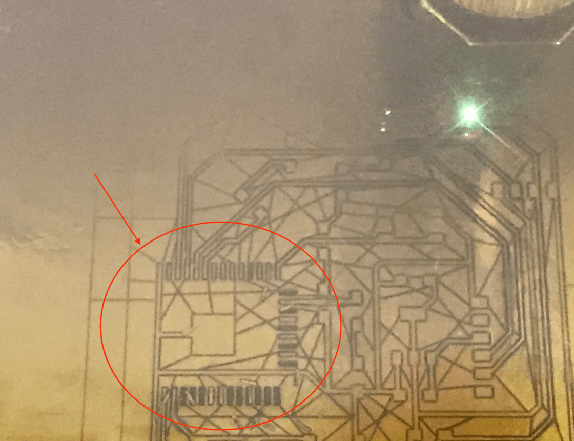
I really liked Option 1 but I was not sure which components I should choose to keep with the ESP32. I assumed the components that were on Neil's example would all be crucial, however keeping them all on the FR1 board might not make the overall system as flexible as I wanted it to be... After some internal debates, I chose to first do a test cut on an ESP32 before making a final decision. I followed Spencer's documentation to set up the fiber laser for flex PCB.
After some experiments, we found that the original settings (P: 65, V: 1.2, Frequency: 2000, Pass: 1) were high on the ESP32, thus, we lowered the power to be 50 and velocity to be 0.6. Yet, the next challenge was weeding:
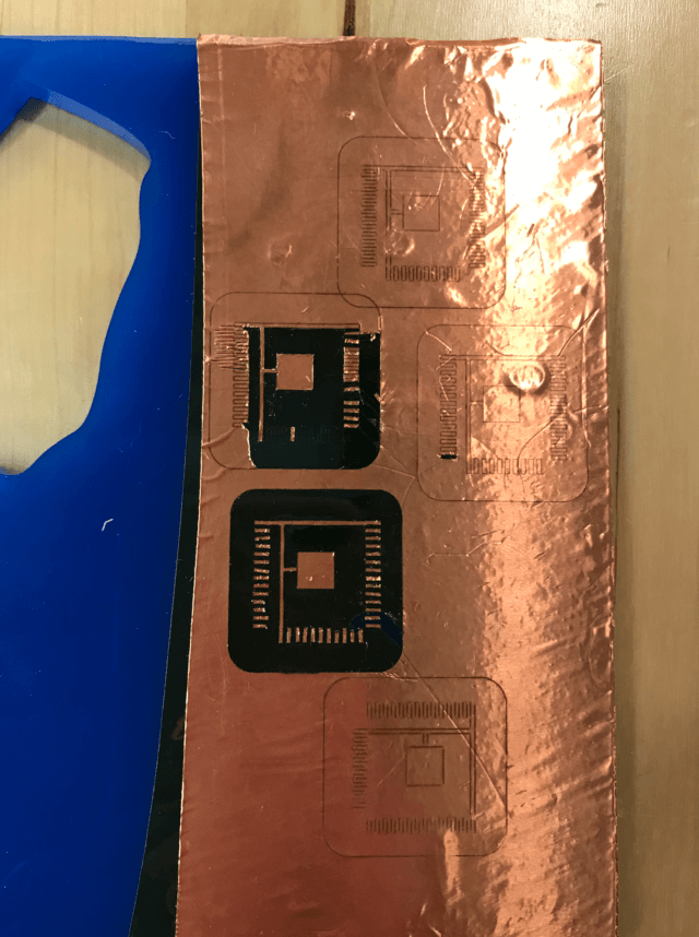
Eventually, I was able to find the right tool and right angle for weeding the copper vinyl.
May 24, 2021
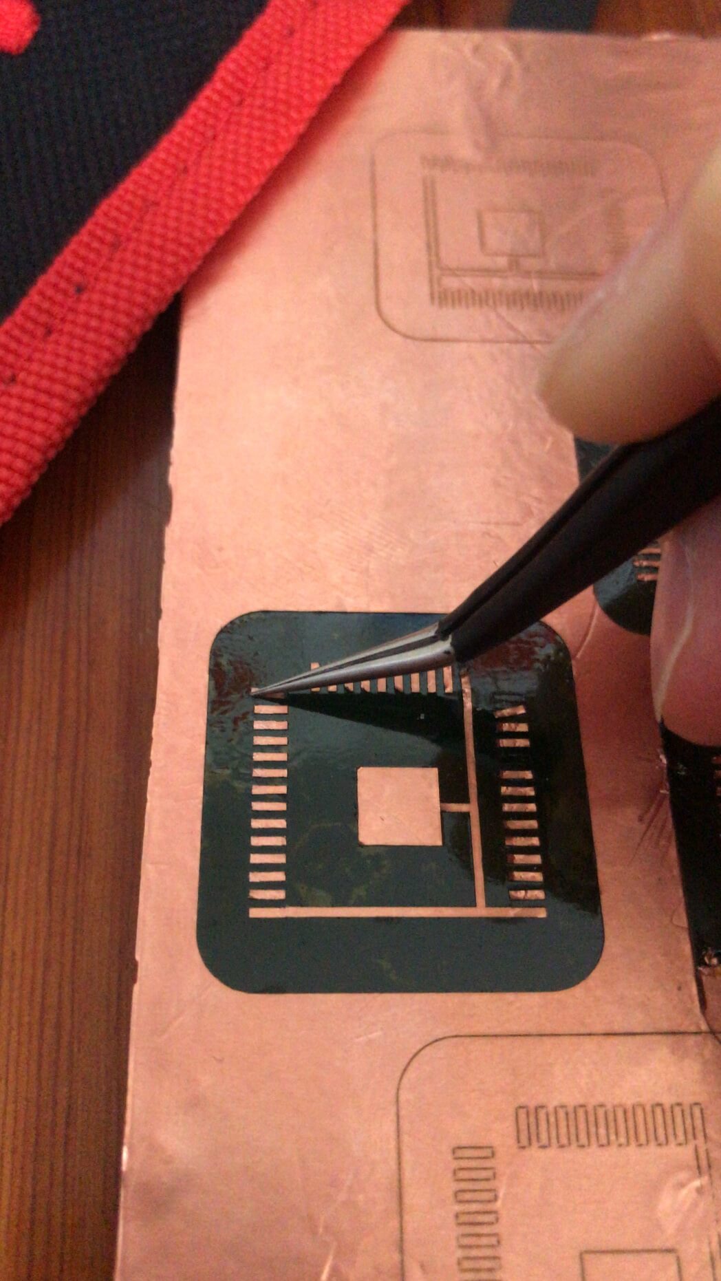
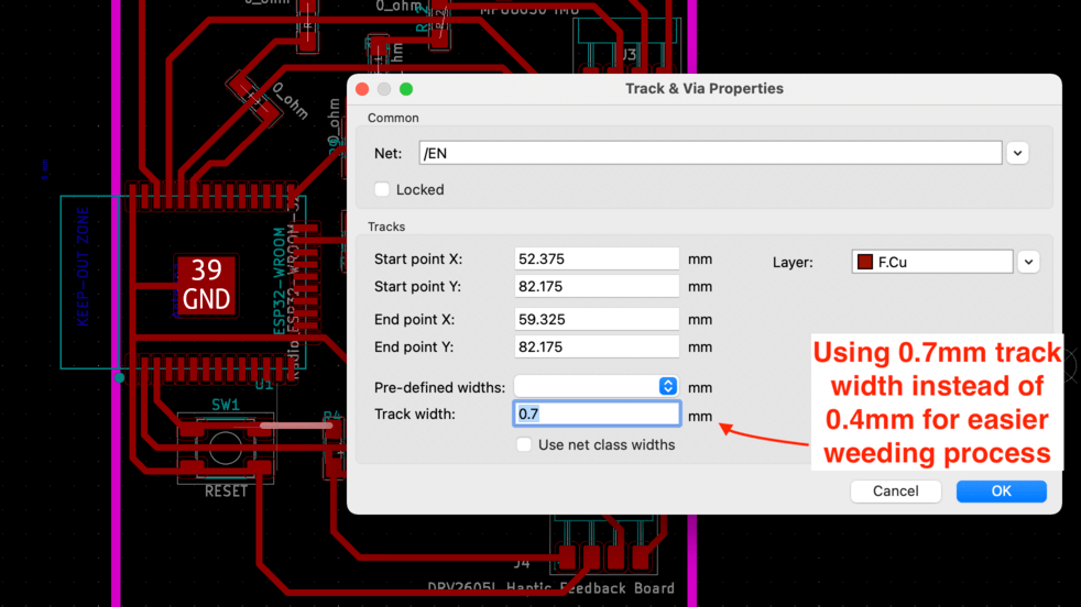
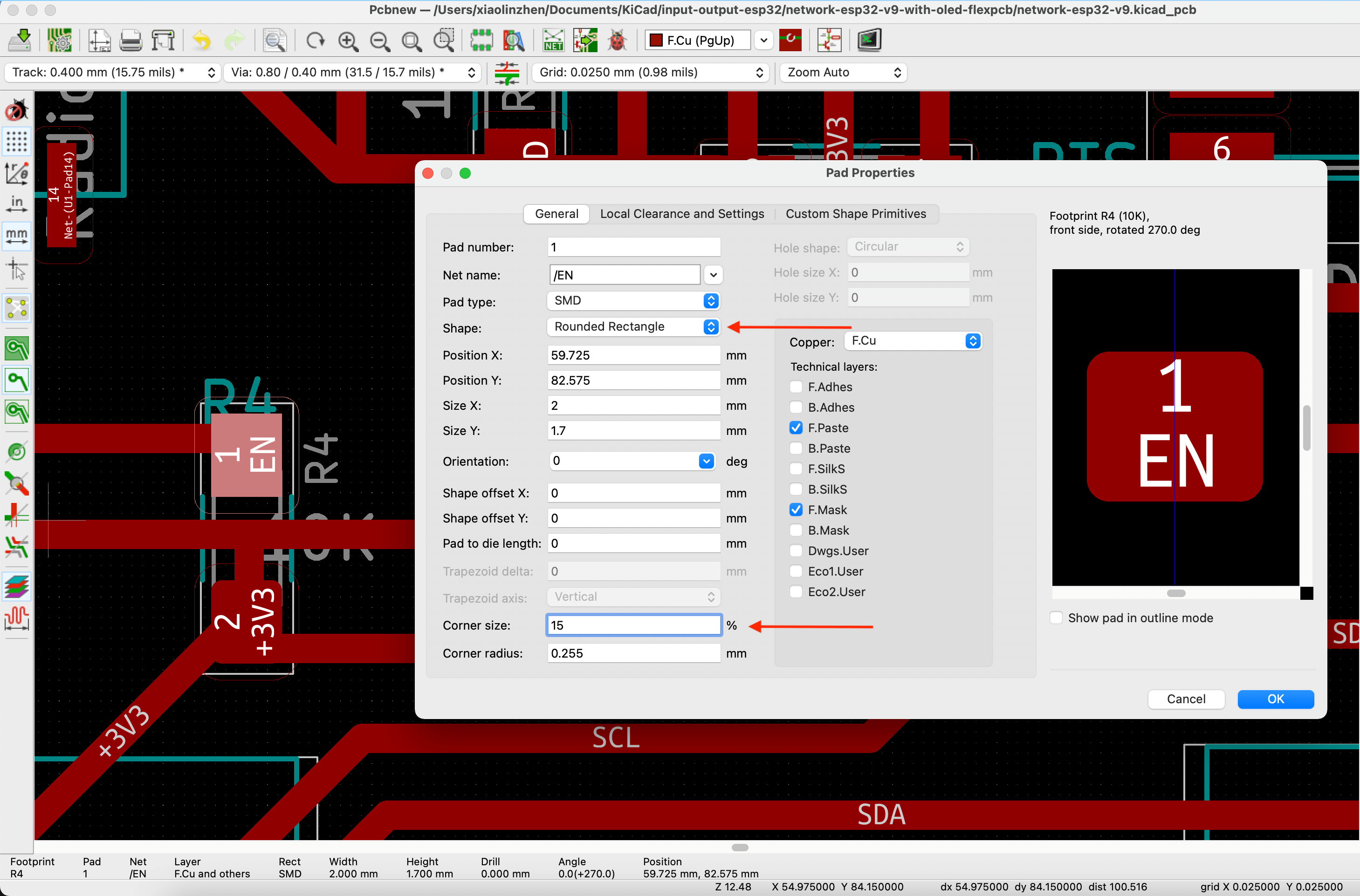
Thanks to this exercise, I felt more confident on making the whole PCB flexible. Here are some changes I made on my PCB to help with the weeding process.
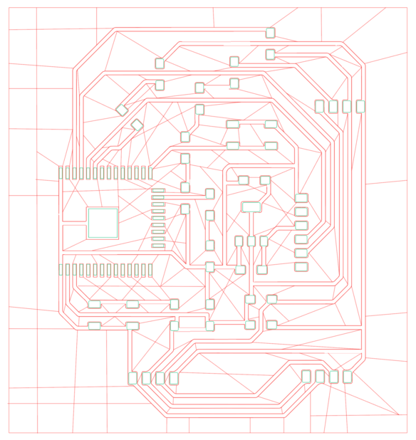
Part 1: KiCad
Part 2: Adobe Illustrator
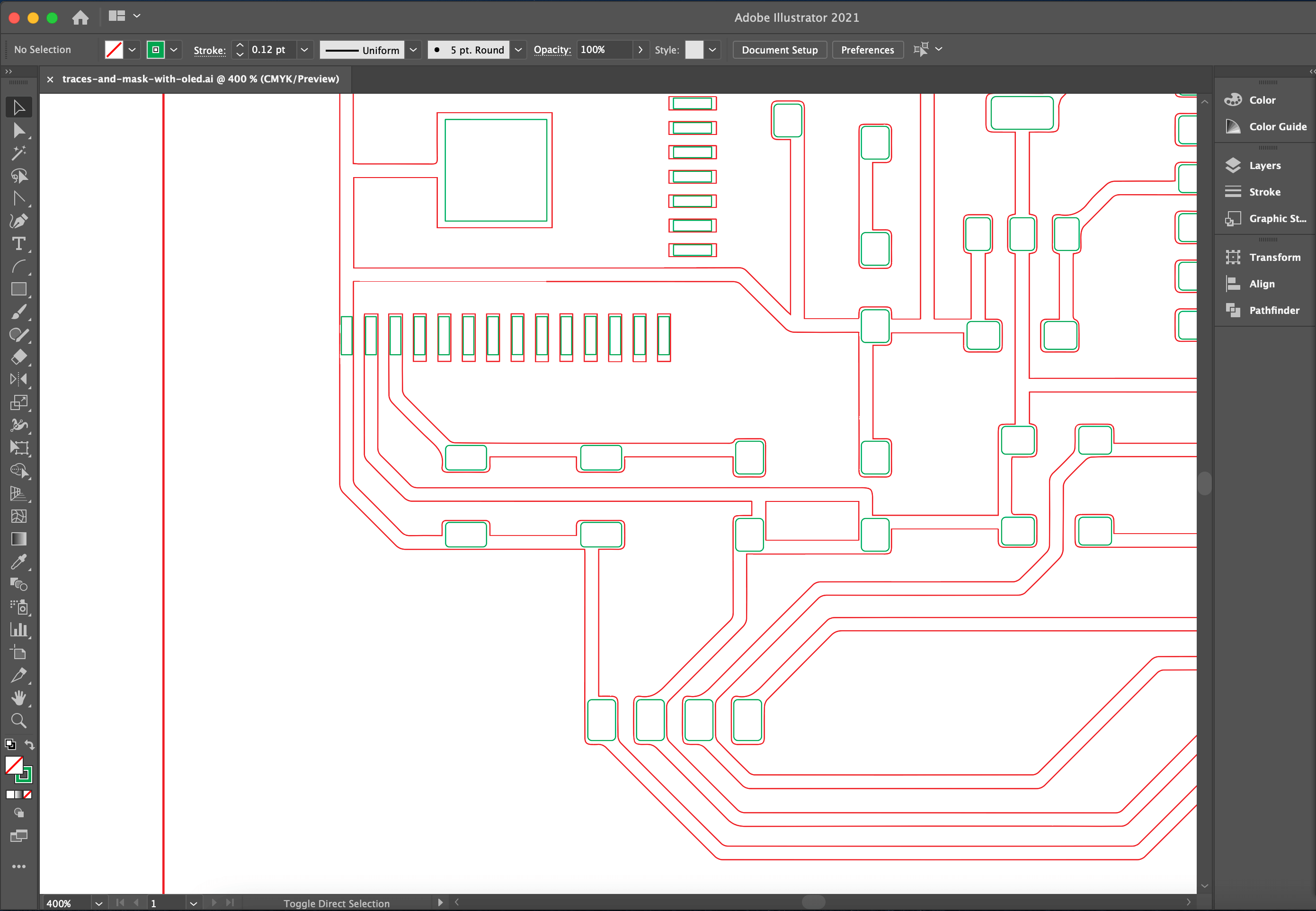
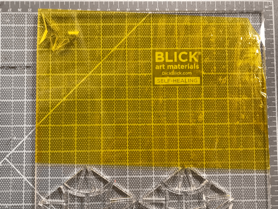
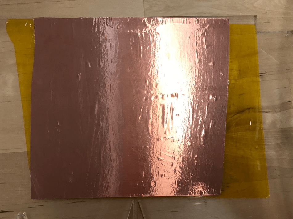
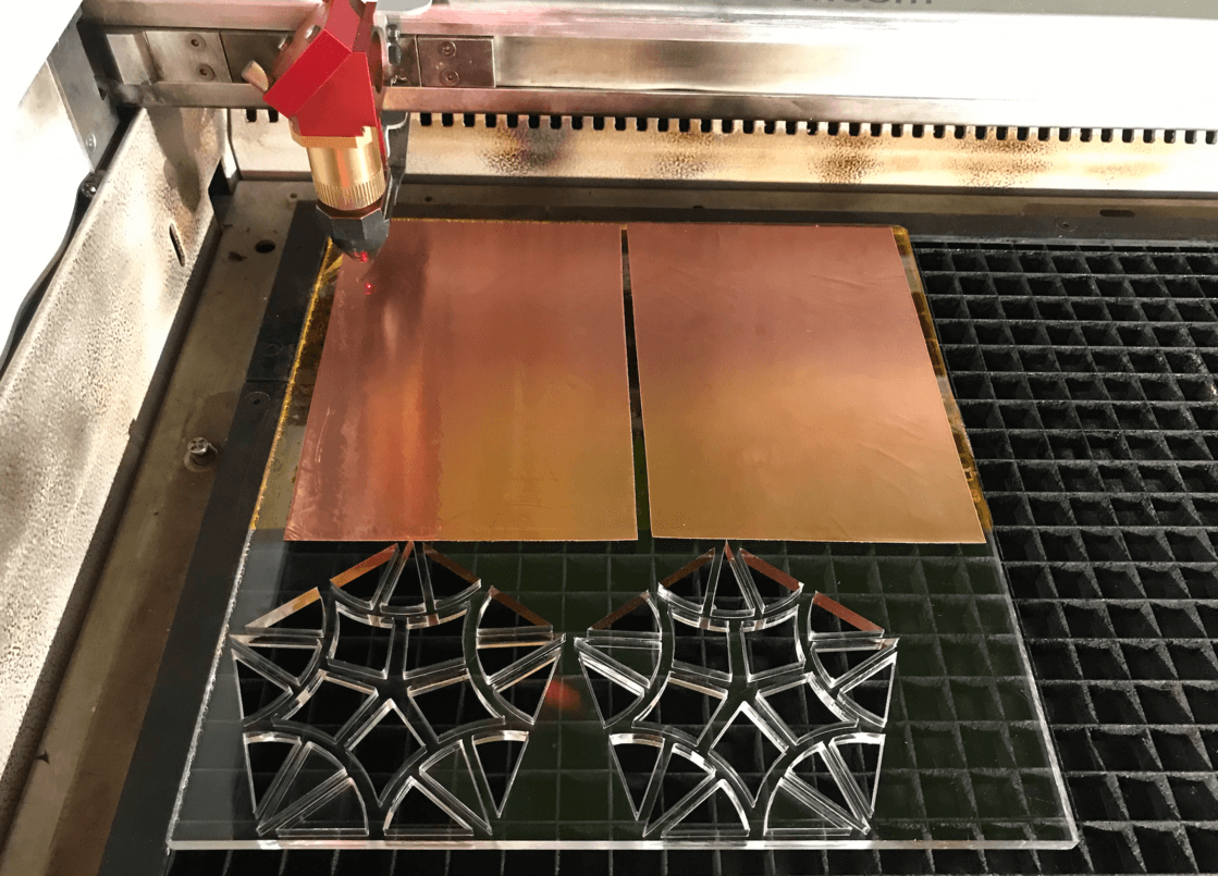
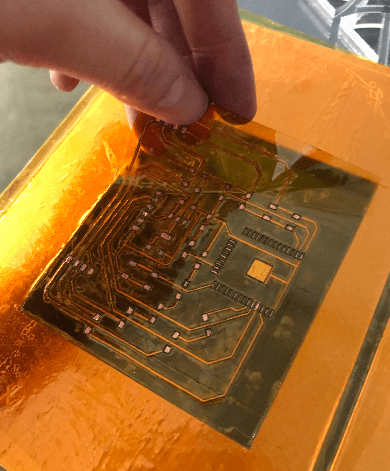
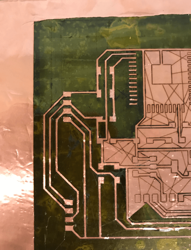
Part 3: Laser Cutting the Board
Here is a short video of cutting the copper vinyl.
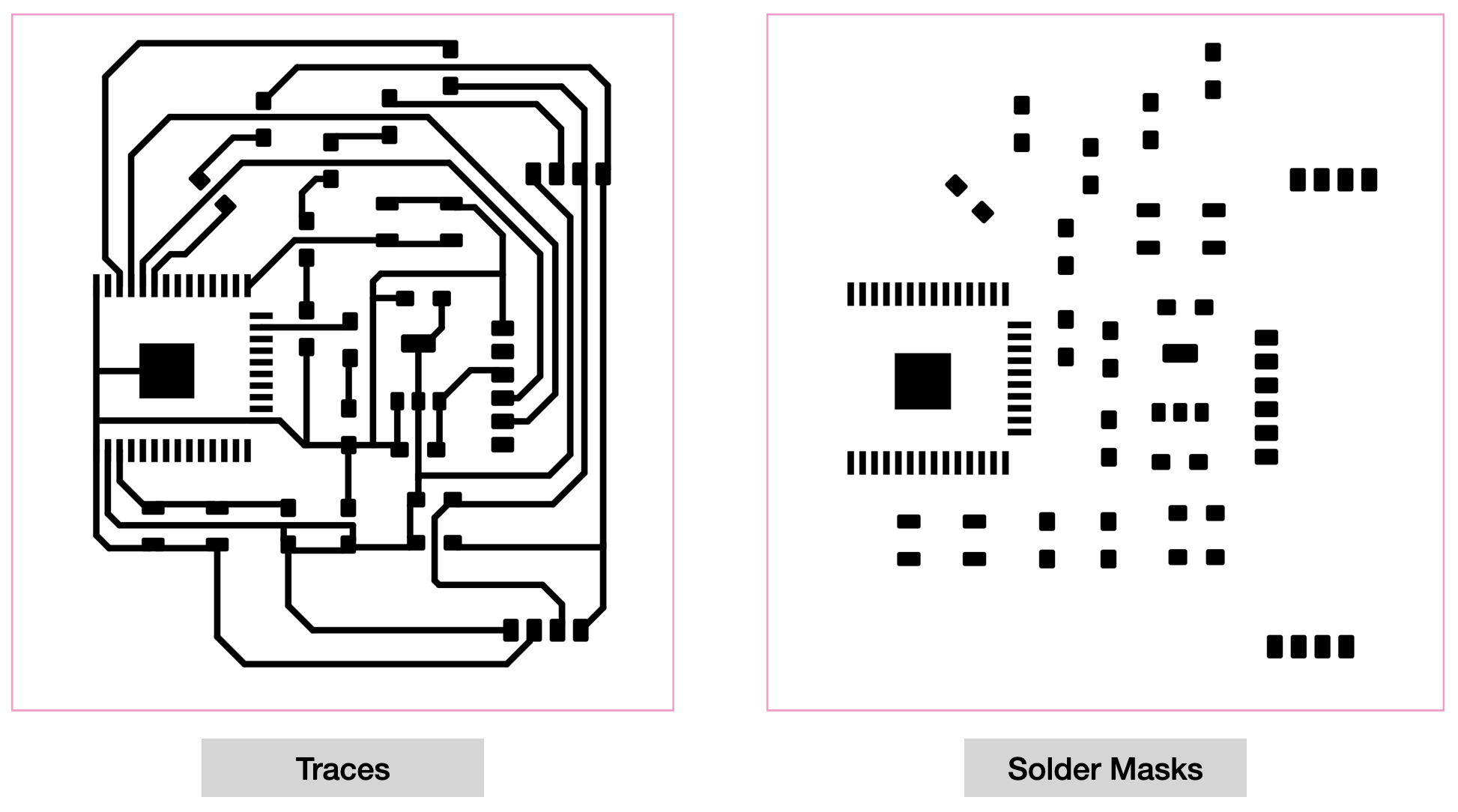
After I removed the scrap copper, I then lay a layer of kapton over the traces. Here is a short video showing the cutting process for the solder masks.
It is suggested to remove the PCB from the acrylic before soldering.
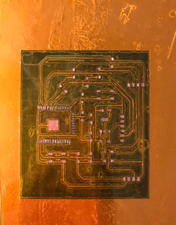
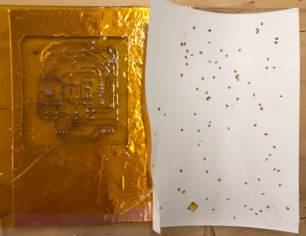
However, I burned some copper pads on the ESP32 so I had to make a new flexible PCB.
Part 4: Debugging and Testing
May 25, 2021From this experience, I learned that weeding plays an important role for soldering. I noticed that I had some difficulty weeding the 90 degree corners, so I reviewed my .ai file and make adjustments on the weeding lines. Spencer had suggested me to keep an extra set of I2C pads on the board in case one of the other two didn't work out.
Eventually, I settled down on one of the boards and started weeding.
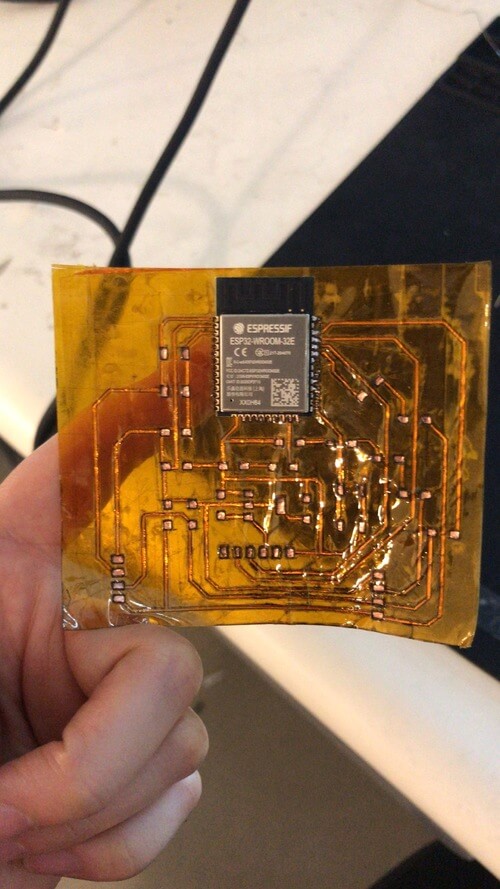
Before removing the PCB from the acrylic, I chose to carefully clean the board with soap water because I thought it was easier for me to find the copper pad. Next, I was ready to solder. To begin, I taped the PCB on the solder mat. I also taped the ESP32-WROOM for better alignment. The modified footprint allowed me to solder this component using the regular method.
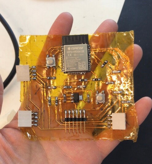
Next, I tested my I/O devices using Adafruit's Arduino examples. Here is a short video showing the I2C communication works for the vibration motor.
Jun 4, 2021
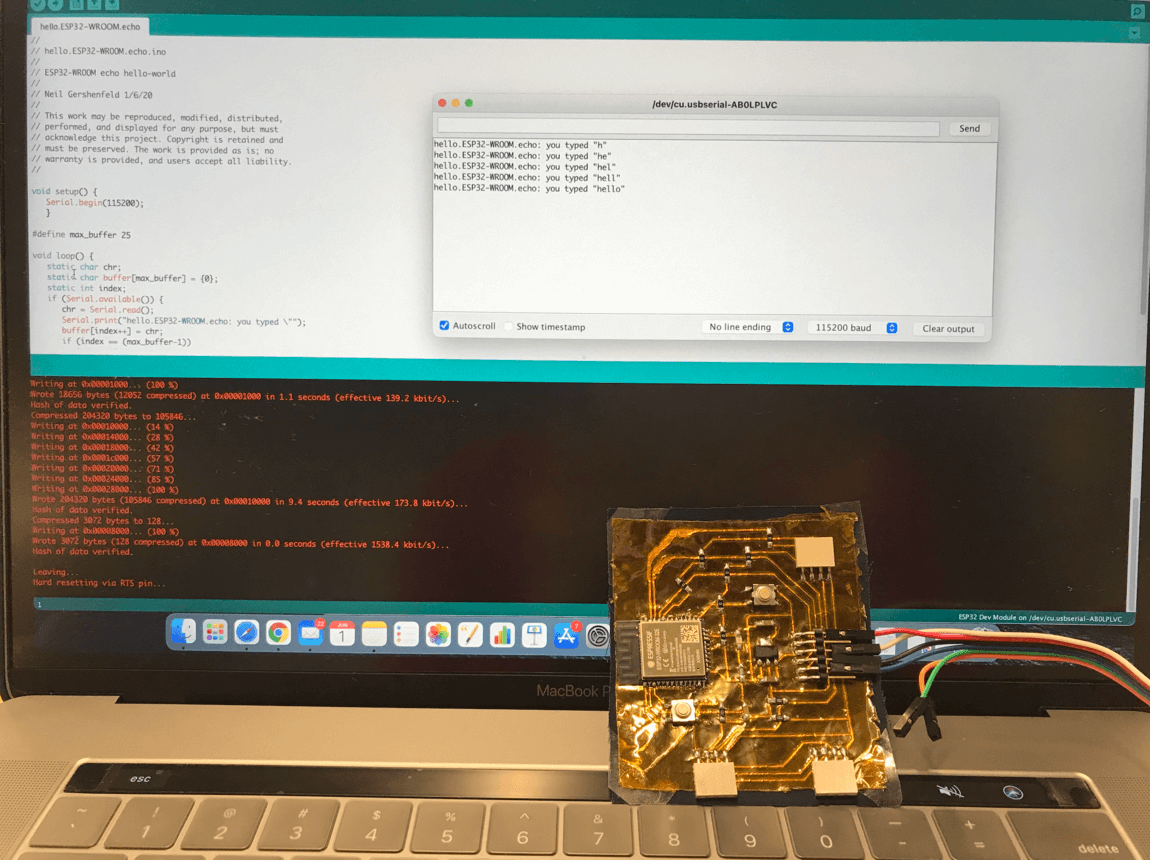
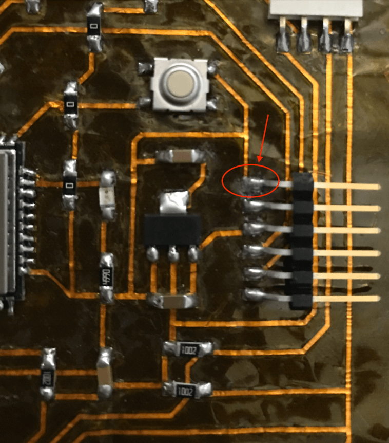
While working on the networking code for my board, I noticed that I kept receiving the error of Failed to connect to ESP32: Timed out waiting for packet header. I then tried the sketch on my FR1 board but it worked. I decided to do a continuity test and found that the GND pad of the FTDI was disconnected. I took a closer look and found that the pad was coming loose, thus I would need to resolder the pad and test again. I also would like to desolder the 4 position headers and solder the modules directly on the board, since that would make the system more compact.
Jun 7, 2021
Part 1: Desoldering
During the office hour, Spencer taught me how to fix the board and also desolder the headers from the flexible PCB using a heat gun. I forgot to take images when he showed me, but the basic process is as follows:
- To fix the pin headers: Spencer used a tweezer to remove a tiny bit of the Kapton mask around the pad to expose some trace, and then connected the pad with the trace. This method helped secure the pin header and passed the continuity test!
- For desoldering: Spencer suggested to hold the header using a long pair of tweezer and lifted the board, then he blew the area (of the header) with a heat gun. In order not to overheat / burn in the area around it, he made sure to move the heat gun left and right. In a minute or two, the tin around the pins started to melt and eventually, the board droped to the table (gently) due to gravity.
Part 2: Making a Second Flexible PCB
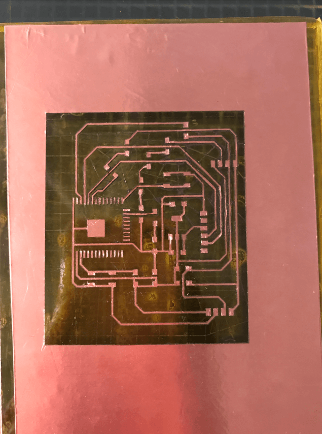
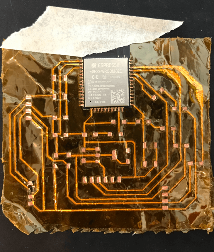
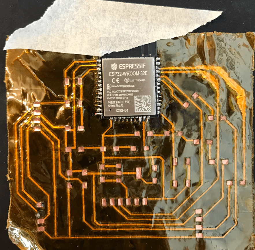
I also seized the chance to make a second flexible PCB. As I already had some experience by then, the process was smooth and it took much shorter time to achieve one. The result was beautiful to me! Here is a short video showing the process and the result of the second flexible PCB. In this PCB, I used a slightly larger power, so the setting that I used for the fiber laser was: P: 55; V: 0.6; Frequency: 2000; Pass: 1.
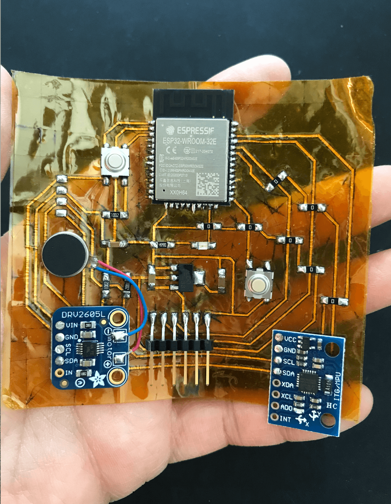
And here is a hero shot of the final flexible PCB, I was very happy with the result!
Files
Please find below the files that I made for this assignment.