7. Electronics design
This week I designed an Attiny412 board, Manufactured it and finally tested it.
Circuit Design
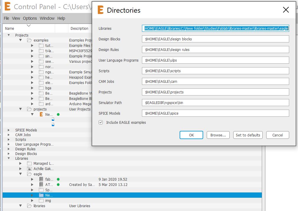
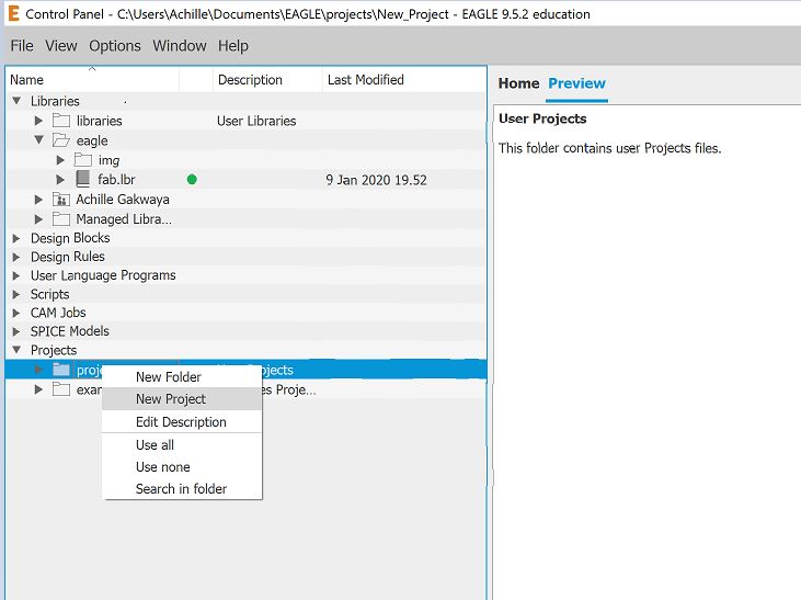
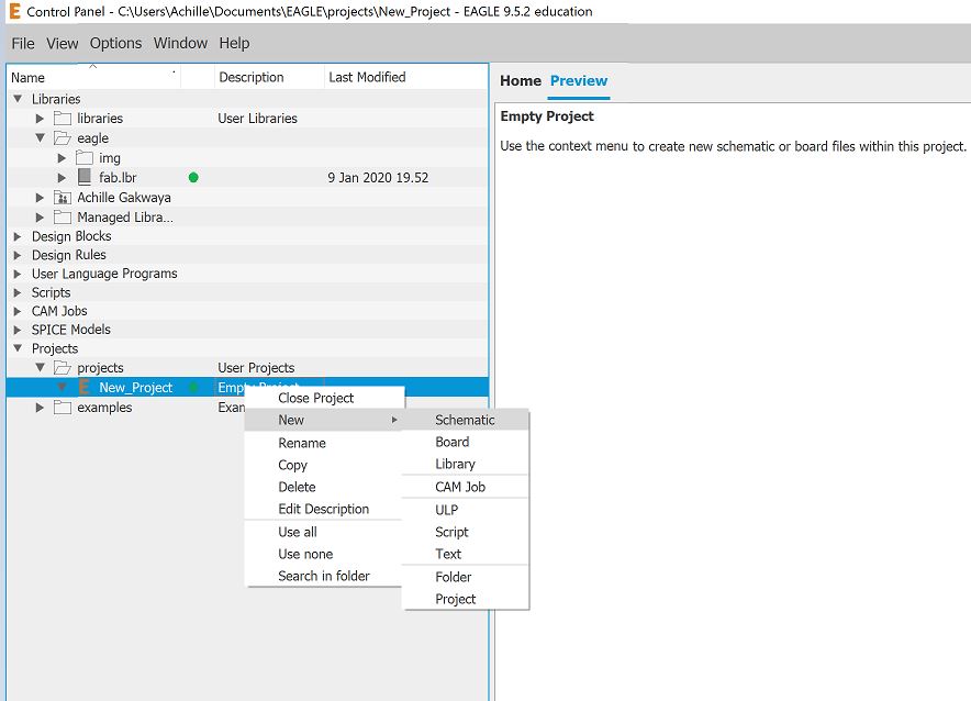
First I got the original design and used Eagle and Additional libraries. The latter was added to Eagle by copying it’s directory as shown in the image. Next after the libraries appeared I clicked on the dot next to it and made it green (active). To create a new project I went to Right click Projects>New Project and to create a new schematic Right click on the new project and the selectNew schematic.
 Original design
 Addinglibraries
 Creating a new project
 Creating a new schematic
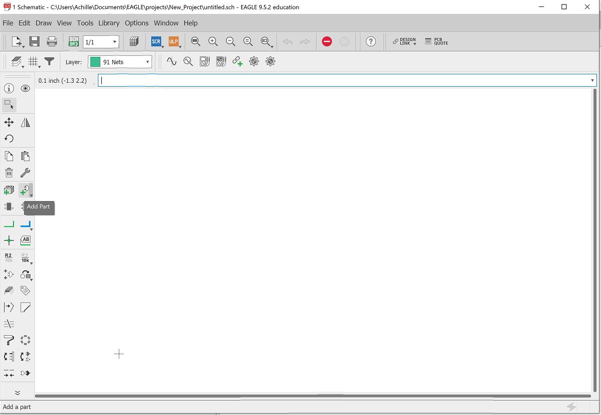
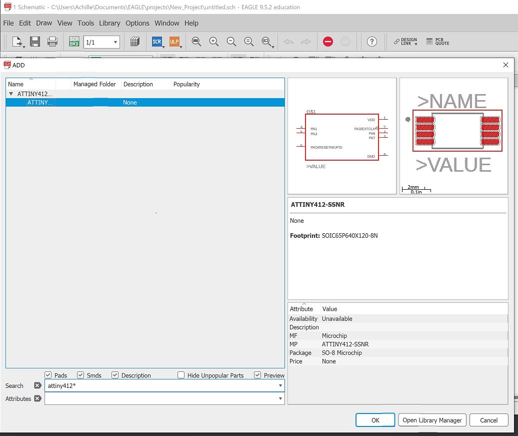
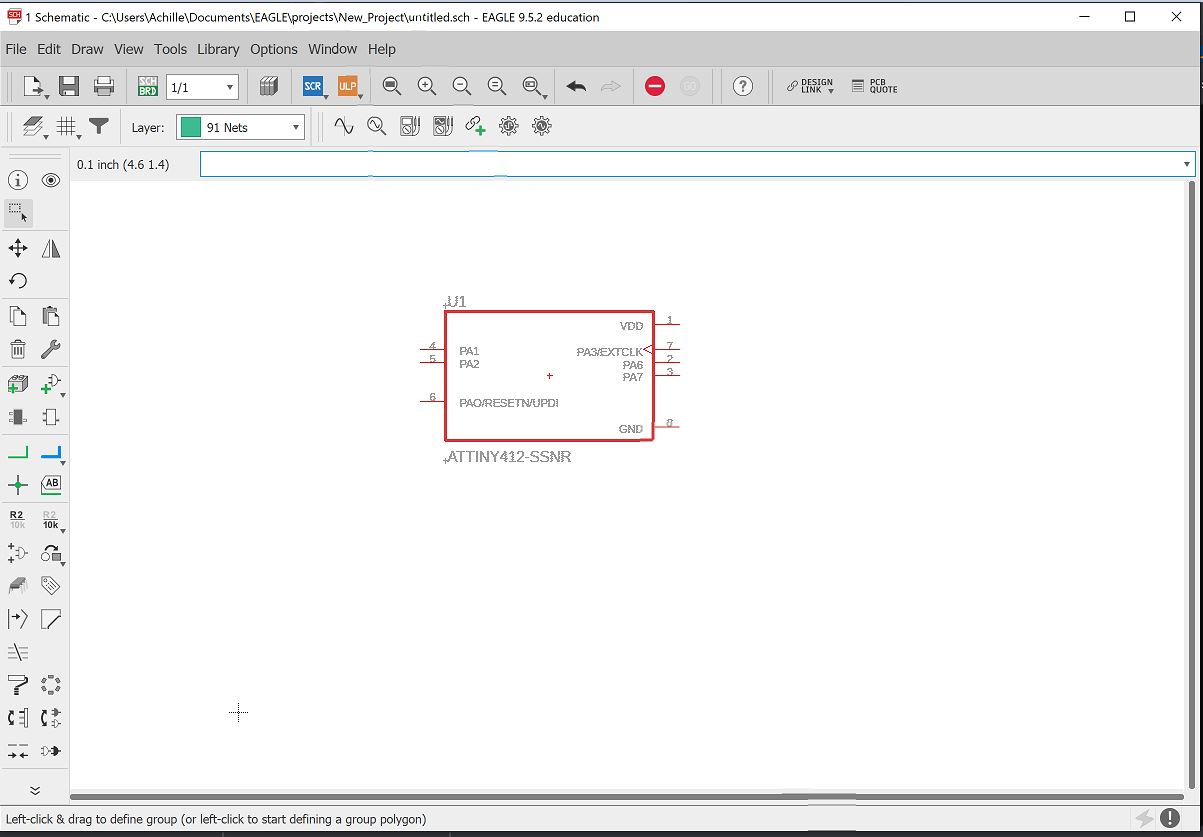
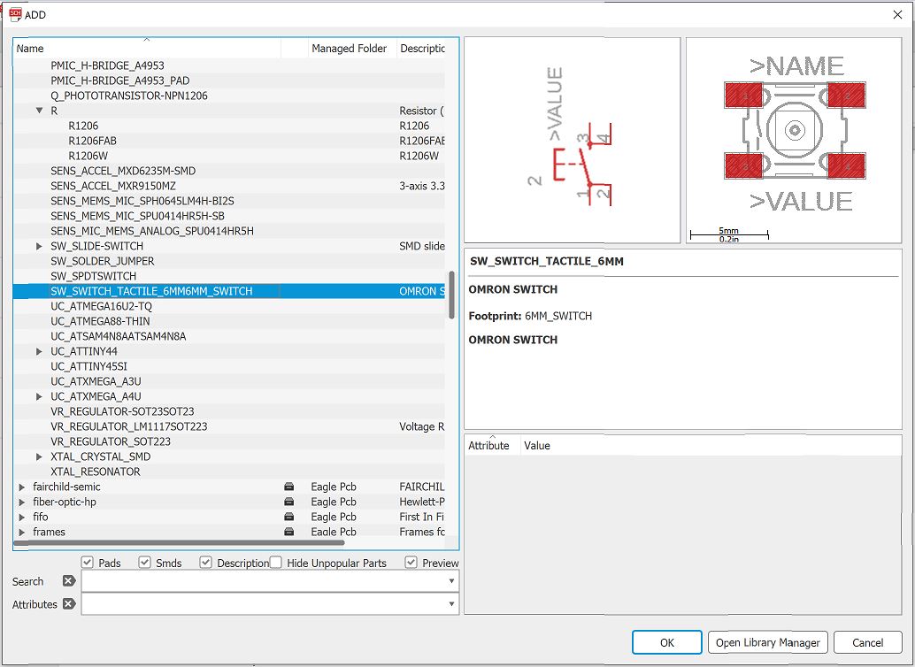
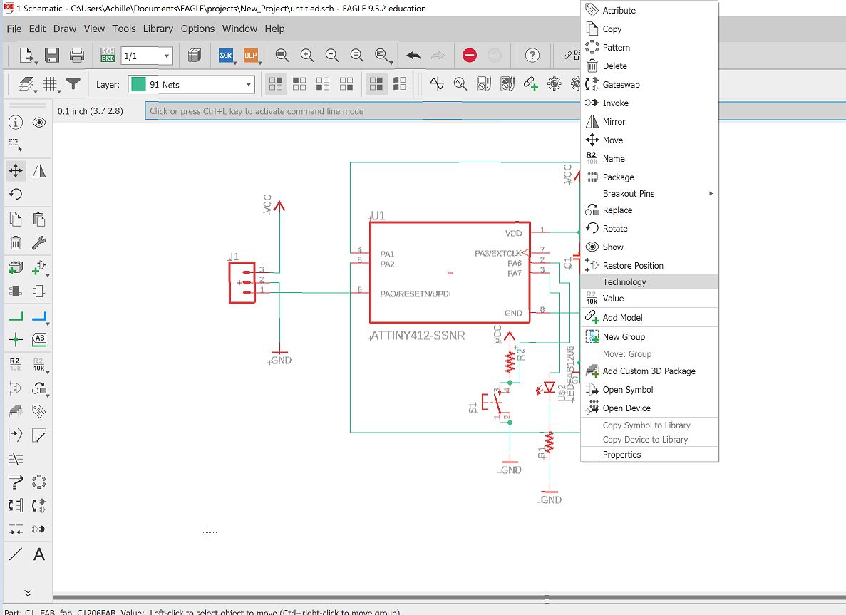
Now that I had a workspace I could add parts by clicking on Get part (as shown in picture). Then I proceeded to selected the ATtiny412 processor whose library was obtained from here. Next, I added the remaining components like resistors, capacitor, push button and diode. After all these were added I started connecting the components as per the original design.
 Adding components
 Search processor part
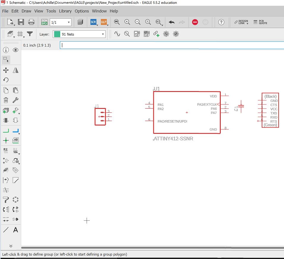 Added ftdi and 3pin connector
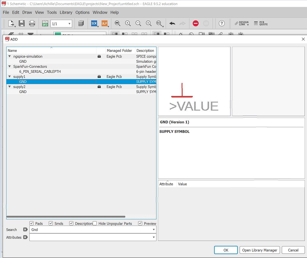 Add ground
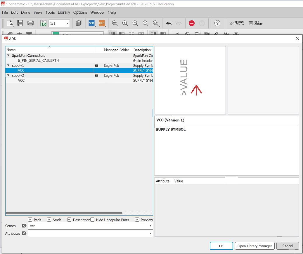 Add Vcc
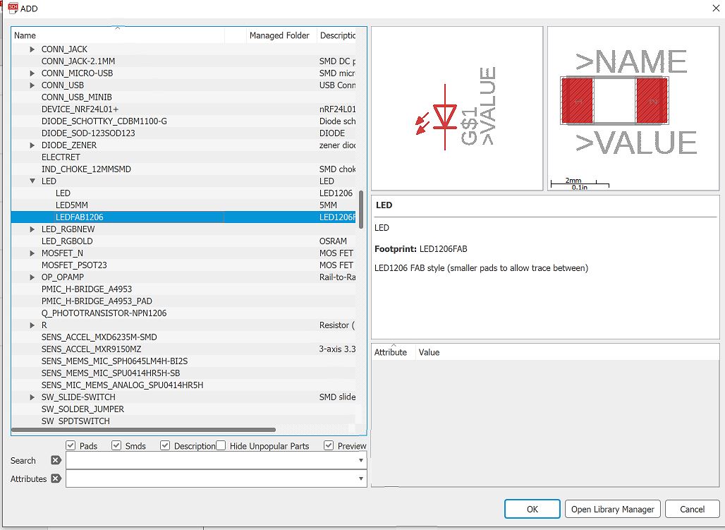 Add diode
 Add push buttton
 Changing component value1
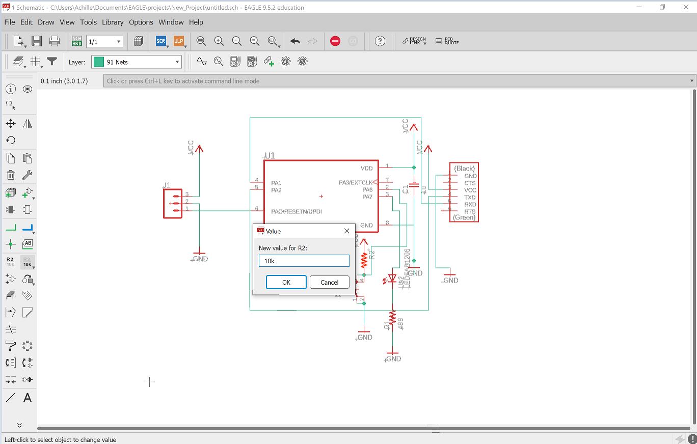 Changing component value2
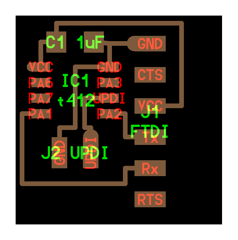
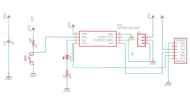 Final Schematic design
I should point out that the ATtiny 412 processor we got at the beginning of the design was not correct before and we had to get a new one from from here.
After the Final schematic was drawn, I proceeded to do the layout for the schematic in order to design the final PCB. to do that I clicked in the upper left coner Generate/Switch to Board and from there I analysed the Board
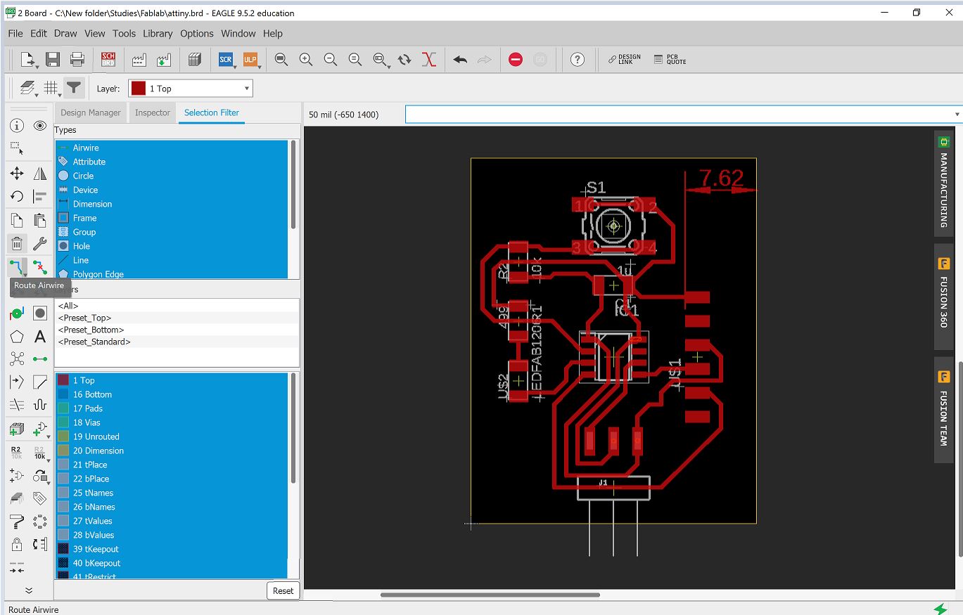
and aligned the components according to the original design. After, this I did routing by clicking on Route Airwire and followed the yellow lines to know where to connect. after the routing was done, I decreased the design window size to a size close to the board and I then
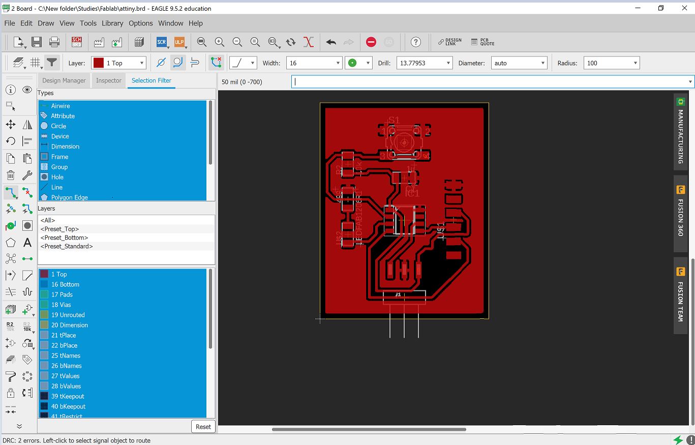
selected Draw Polygon and called it GND to represent ground and drew it along the board’s circumference and then clicked Ratsnest to create the ground in the whole board where it’s applicable.
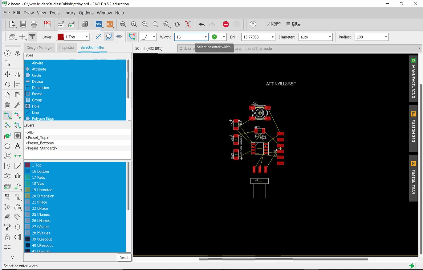
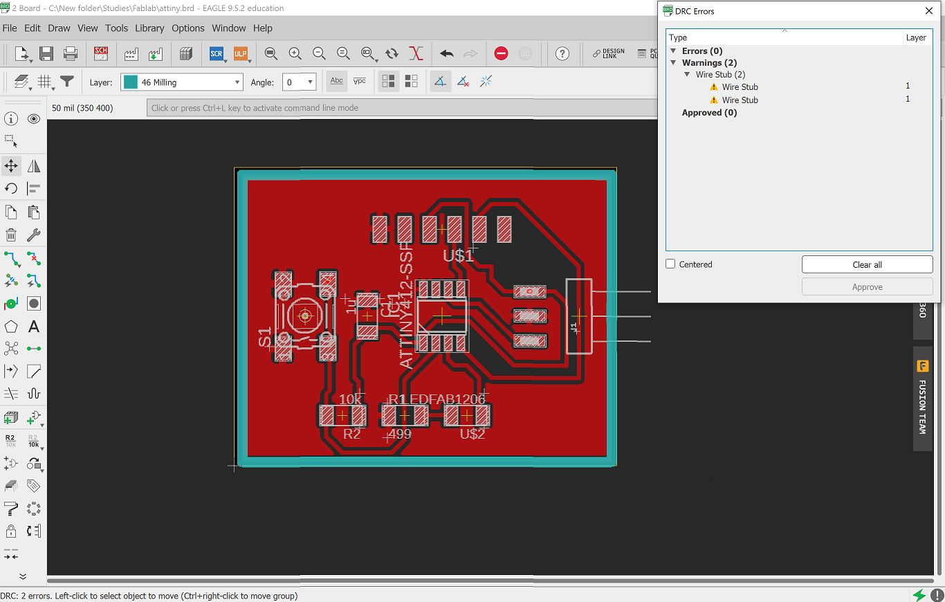
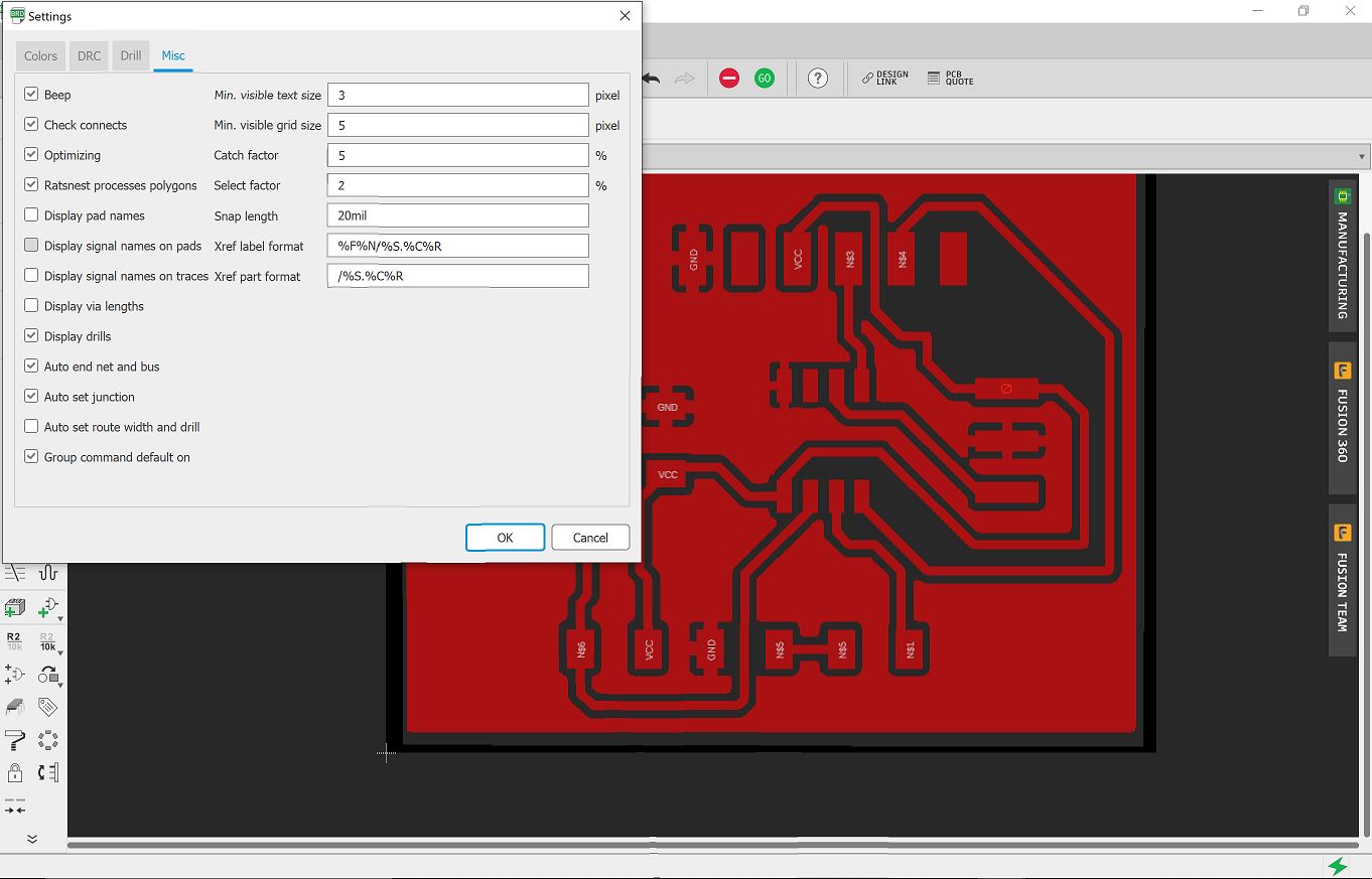
Next I modified Design Rule check (DRC) settings to 16mil (as shown in image). After that I ran DRC to check for mistakes. After this, I proceeded to draw the outline by
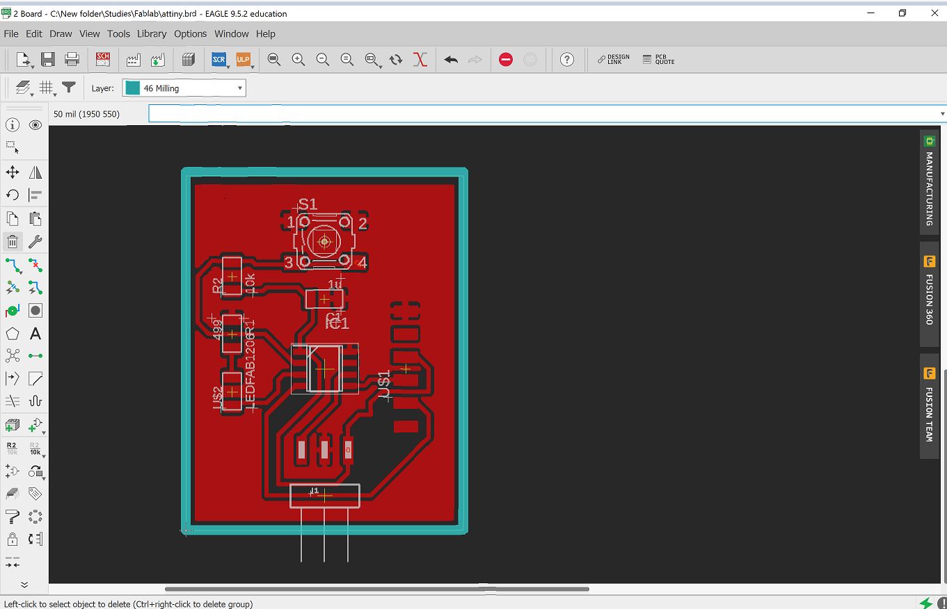
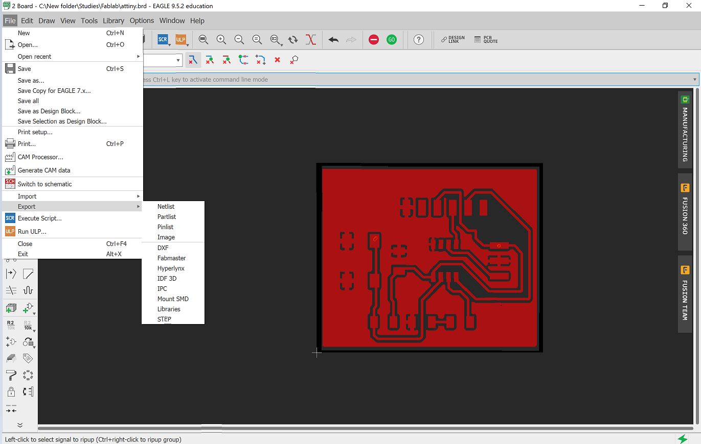
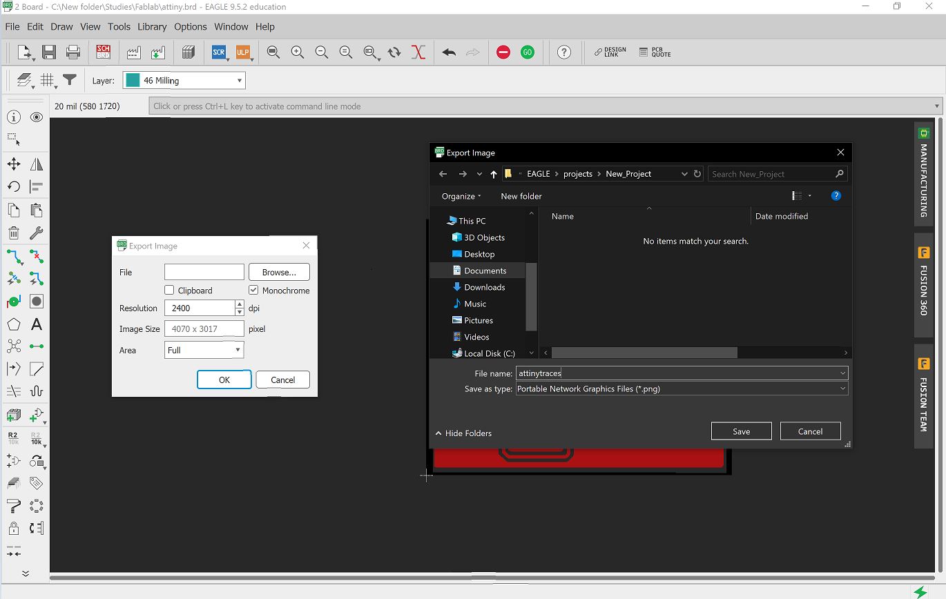
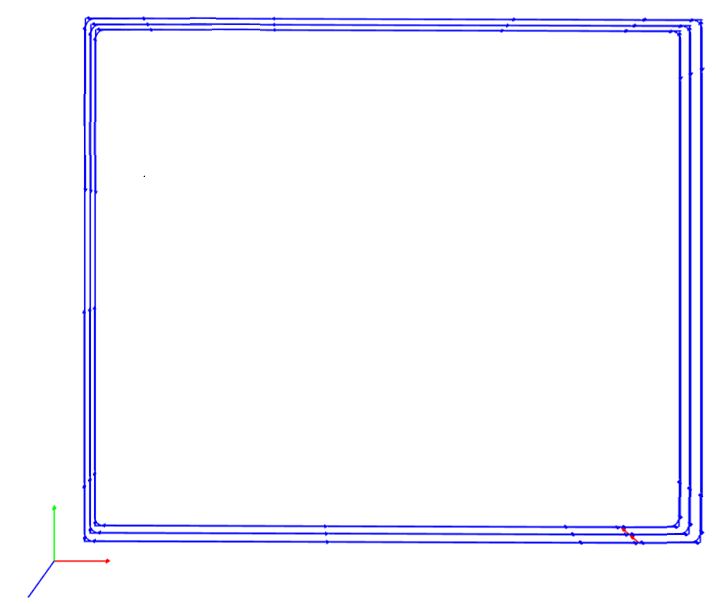
selecting layers and then chose the milling layer then changed it to 40 mil. and drew it along the outline of the board and finally I rotated the board and proceeded to export the final PCB design as shown in pictures. While choosing the size of the board outline I had to measure the distance
from the pin connectors to make sure they have enough space so that some part rests on the board and they don’t get broken(this is shown in image “Distance from connector”)
 Align components
 Routing
 Ratsnest
 Draw outline
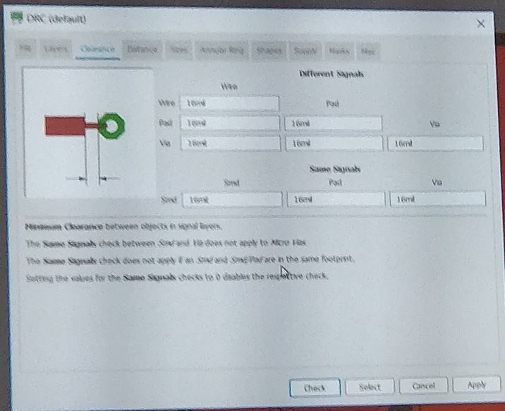 Drcsettings1
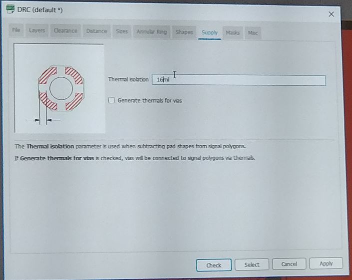 Drcsettings2
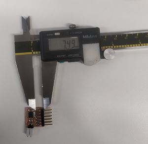 Distance from connector
 Rotateanddrc
 Hide names of components
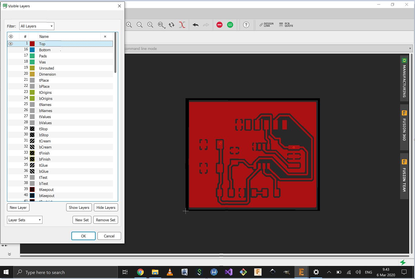 Hidelayers except top
 Exportting toplayer1
 Exportting toplayer2
 Hidelayers except milling Layer
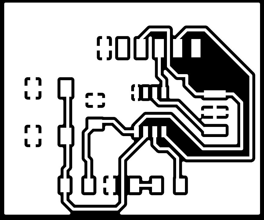 Exported traces
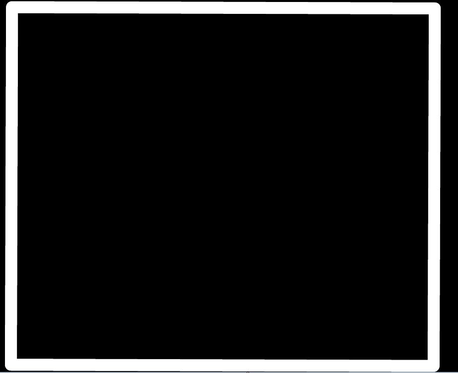 Exported outline
PCB Manufacturing
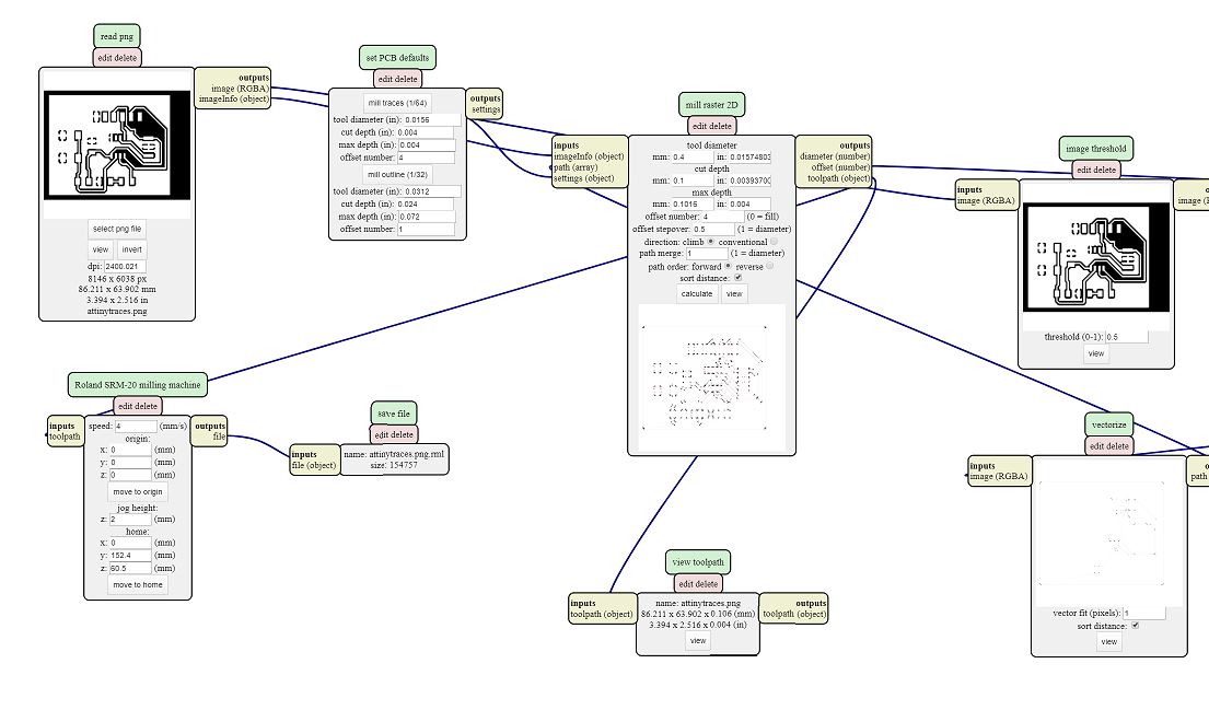
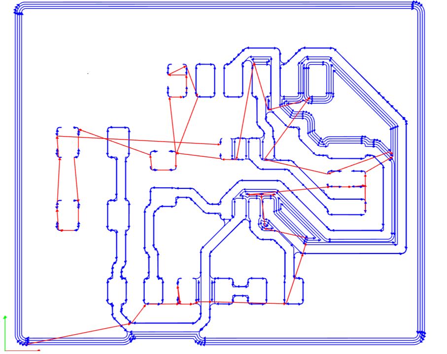
Like previously done I went to Mods and created the G codes for the milling machine.Next, I milled the product(result shown in picture) Then I gathered the components and soldered them on my board and the result looks as shown in the picture. while working with Mods I noticed that I was getting an unusually large board dimension for Traces and Outline but latter on through the help of our local instructors we managed to change this by changing settings as shown in image Correction below.
 Mods for traces (large)
 Correction
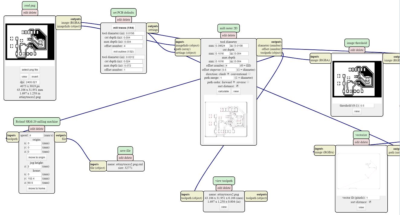 Mods for traces correct
 Mods traces toolpath
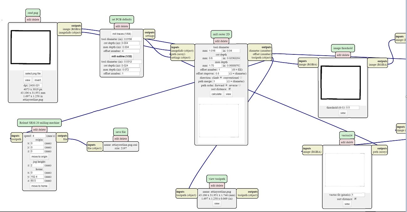 Mods for outline
 Mods outline toolpath
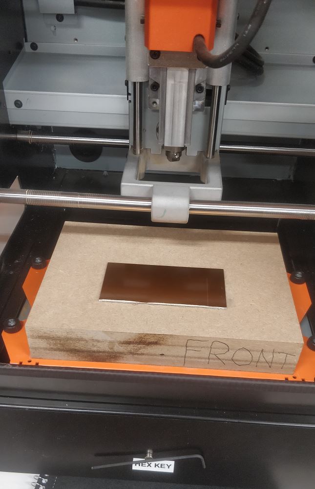 Milling
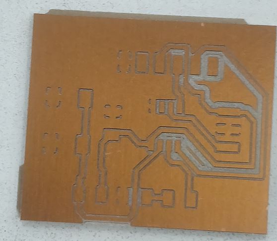 Milledproduct
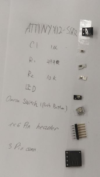 Components to solder
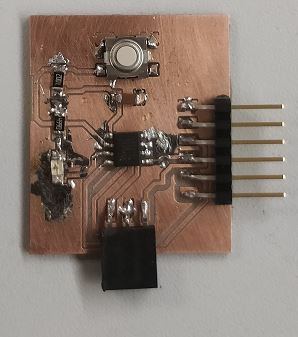 Finalproduct
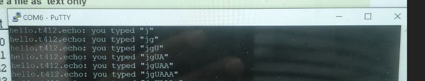
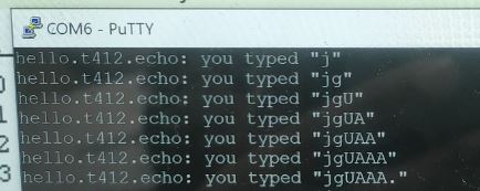
Testing
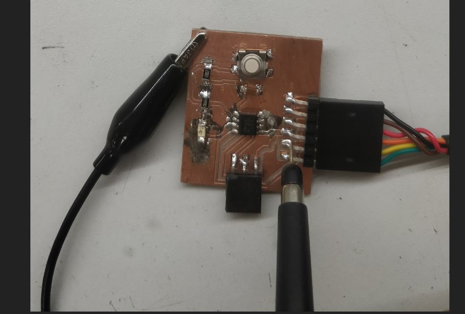
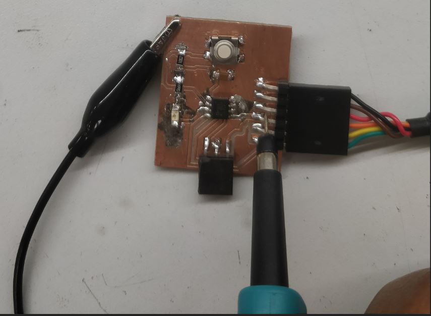
To test the Board I programmed it using my previously manufactured Programmer and uploaded the Echo and then tested the board as shown in the pictures. Detailed steps of the Board programming are explained here.
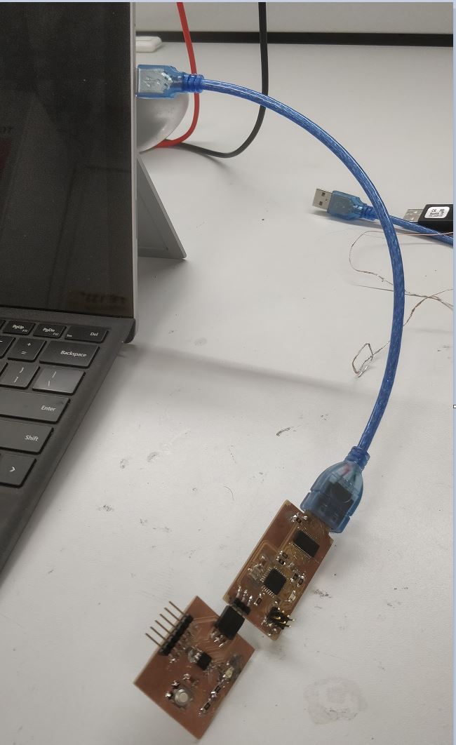 Programming ATtiny
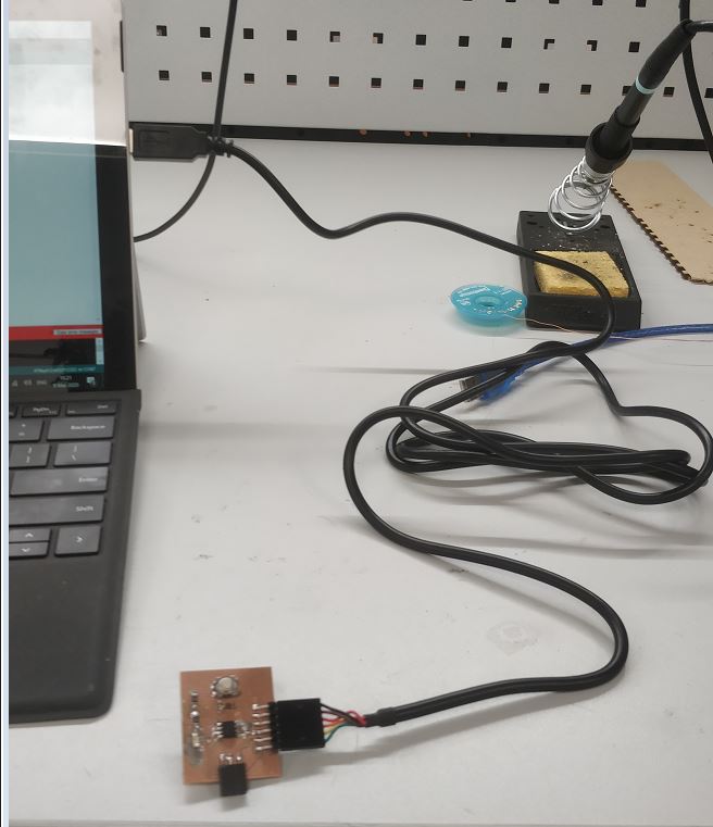 Testing ATtiny
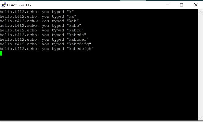 Finaloutput
Group Work
In the group work we use the Oscilloscope to read charcaters that are sent to or from the ATtiny. we also calculated the time duration of all characters sent to see if it matches with that on the Oscilloscope.
The members of the group: Achille , Anssi , Jari , Hannu .
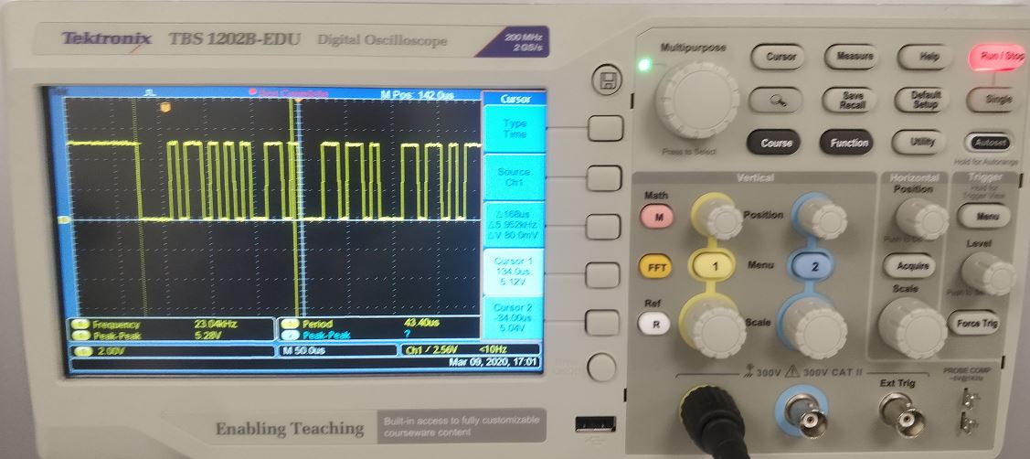
We started initially with the ATtiny connected with FTDI cable to the omputer, then we used the Oscilloscope probes to connect the board’s Ground and Rx pin as shown in picture. AFter that we interpreted the signals on the Oscilloscope’s screen using Ascii Table and made use of the rule of the UART protocol which ATtiny and the computer use. As shown in the picture the signal on the Oscilloscope represents character ‘A’ which is according to asccii 41 in hexadecimal or 01000001 but since the rules of the protocol state that there’s a start bit which is ‘0’ and then 8bit data sent with LSB first follows and ends with a logic ‘1’ stop bit. We used this and found out that the data matched the ‘A’ that was just typed.
ATtiny Setup
 Probes on the Ground and Rx
 Sent character from the Computer
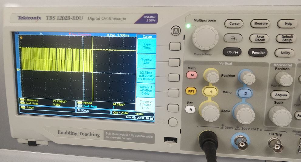
Next, we changed the probe from Rx pin to Tx pin to read the characters that were sent to the computer. As shown in the image the text sent by the ATtiny starts with hello and therefore ascii for ‘h’ (68 hexadecimal) shoulbe at the beginning according to the protocol it comes out as 00010110 and is confirmed to be matching the bit pattern on the oscilloscope. Next, interesting thing to measure is if the characters sent match the time duration on the oscilloscope as shown in the image the last characters are 31 in number and the duration for a single bit is 9 usec and according to the protocol one character is sent in a frame of 10 bits which makes it 109=90 usec duration for one character, therefore time required to send 31 characters would be 9031=2.79 msec which closely matches the value onthe oscilloscope.
 Changing setup to read characters sent from ATtiny
 Characters sent
 Bit pattern of ‘h’ character from hello
 characters duration
Files
(Board/Schematic/Traces rml/Outline rml/Traces PNG/Outline PNG)