7. Electronics design
Often in electronics education, there is a lot of “rote learning” involved, without a proper introduction to the rich history that resulted in a variety of electronics revolutions - i.e. the vacuum tube, the transistors or semiconducting devices etc. upto what we have today.
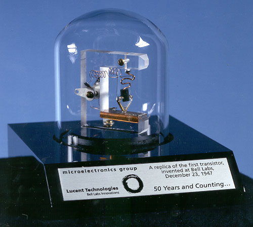
I checked some documentaries on electronics to satisfy this curiosity - on how Bell Lab scientists invented transistors, the impact of the electronics revolutions in the future of globalization, the Japanese tech revolution with transistors,the evolution of computing and so forth - These narratives felt especially inspiring to take up against this daunting task now.
Considering my tentative final project is to be based completely on the design of electronics, I felt the need to create a knowledge repository.
Here is a small list of what I started out with as bedside reading material:
The books :
Resources On Electronics -
The Hitchhiker’s Guide to PCB design
A great inside look at the PCB manufacturing process within a large company - with tacit wisdom.
Art of Electronics - Paul Horowitz
The ultimate book on electronic “design” according to most hardcore-tronicers - with a thorough overview on fundamentals.
How to Test Almost Everything Electronic - Delton Horn
A great book for testing electronics in the lab.
I found great documentation for Learning Ki-Cad both as PDF Resource as well as Digikey’s Ki-Cad YouTube channel.
Online Resource:
Sparkfun had a very nice overview to the world of electricity, using very good analogies.
The site also had a lovely page about voltage, resistance, current and Ohm’s law - they were explained using a water tower as an analogy.
“When describing voltage, current, and resistance, a common analogy is a water tank. In this analogy, charge is represented by the water amount, voltage is represented by the water pressure, and current is represented by the water flow. So for this analogy, remember:
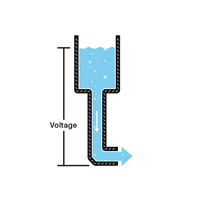
“Water = Charge Pressure = Voltage Flow = Current”
In this way, the formula for deriving the resistance of a circuit is determined by the following:
PCB design, which is major part of this week’s assignement - encapsulates a lot of advanced knowledge to truly understand where the currents flow in these tiny microcosmic circuits.
In the world of manufacturing, there are established workflows for successful PCB design - every decision incorporated into the design feeds the success of the ensuing steps.
This week the central assignment was to redraw an echo hello-world board.
Group Project
Use the test equipment in your lab to observe the operation of a microcontroller circuit board - using an oscilloscope
Individual Project
  *redraw an echo hello-world board*

  *add (at least) a button and LED (with current-limiting resistor)*

  *check the design rules, make it, and test it*

  extra credit: simulate its operation
This board redesign was a very good exercise in getting familiar with not only the arcane universe around electronics - but also to get familiar with the workflow, tools and resources out there.
The ultimate personal goal with the entire electronics modules is for me to (hopefully) be able to evaluate circuits using quick intuitive “back of the envelope” methods, and not dwell too much on the physics and math of it.
Redrawing the Echo Hello Board
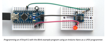
Due to the Covid19 lockdown, and a delay in the projects - initially, the Hello Board and USB-FTDI host board with 5 V power, and long USB cable were provided by the lab for pickup. As a result, I started with embedded programming - and reverted back to this section later on, to design my Hello Board from scratch
Below were the boards initially provided by the lab.
 Hello Board with the AtTiny412 and the USB-FTDI host board powering via USB 5 V
 Programming Board with UPDI (Unified Program and Debug Interface)
What continues below is the process I followed to design and make my own Hello echo board.
Choosing the AtTiny412
Initially, I referred to this Medium Blog, an ATTINY overview blog and an article that talks about the AtTiny’s unique USART (S for synchronous)USART as opposed to UART (Universal Asynchronous Receiver Transmitter) in a process known as bit banging.
Some of its core features are:
A 2/4KB Flash memory, with 128/256bytes of SRAM and 64/128bytes of EEPROM in a 8- pin package
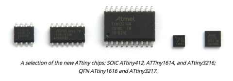
The new ATtiny chips are a new matrix of devices - and they have varying features
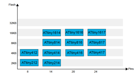
The features are encoded in the name itself.
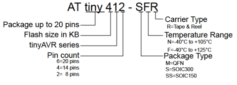
However their real capabilities and differences are only understood by thoroughly going through the datasheet - which is huge. I downloaded the datasheet from Digikey - and went through some of the basics of the ATTINY 412.
A sample programming using arduino and the attiny 412 as a piggyback.
Essentially, the exercise is to recreate a new hello board using the AtTiny 412 with the self made programmer from the previous exercise of Electronics Production week (that used the FX230 programmer chip).
PCB layout for 412 based Hello Board
Initially, the board designs for AtTiny412 HelloBoard were examined.
LED blink board image
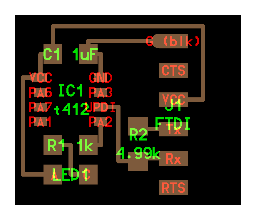
UPDI programmer board image
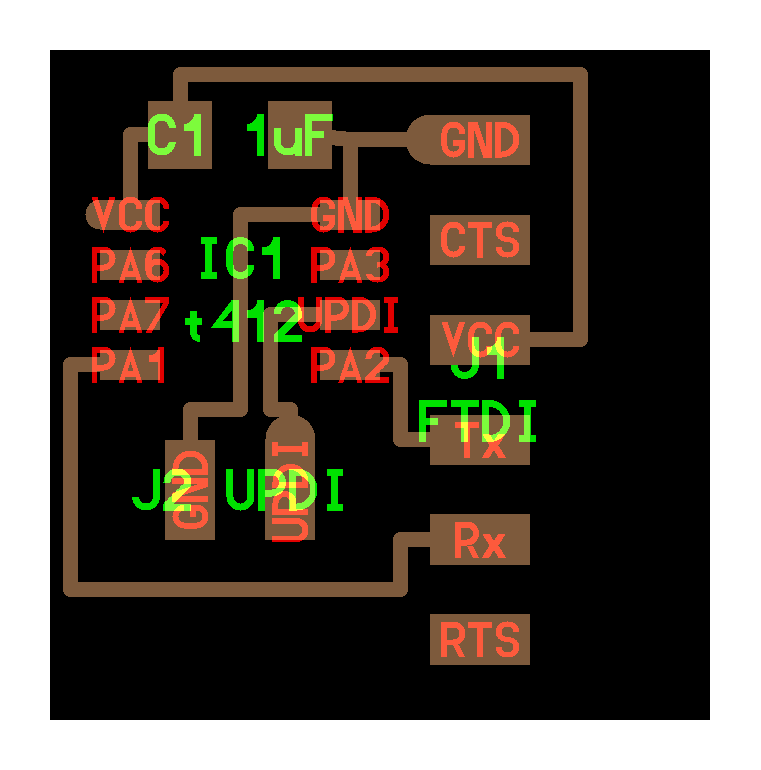
Ultimately, the suggested board design from Fablab that I worked with was a combination of both of the above designs, ie the FTDI I/O pins as well as the UPDI programmer board input pins - as well as switch, one LED one for connection on/off and other for programming blink rates.
Once the board was designed on Ki-Cad, the idea was to test the LED with blink rates.
On Using the Ki-Cad software
Tracing a bit of history, it seems until 1960s (and possibly in India till this decade even!) wires for electronic components, especially in telephone terminals were messily wrapped around posts - and no solders were used. In the 1960s and 70s and commonly in “consumer electronics”, Through Hole technology was used with PTH (plated through hole) - and the solders were applied to the opposite side. Even today, electronic products that need to handle long term impact apparently still use Through Hole technique.
However, Surface Mount Technology (SMT) has no external leads visible, as the leads are milled onto the board - such a board is known as a PCB or Printed Circuit Board. The board is typically made of copper layer with an epoxy substrate if its a single layer, and copper layers on both sides of this substrate for a double sided board.
The goal here is to route / mill copper off the board, in order to establish paths that create the connections needed for our components to establish an electrical signal with each other, as per the design. It is precisely this milling design that is being created with the help of Ki-Cad software (another CAD program, except this is exclusively for PCBs).
The Ki-Cad software is divided into different modules for each step of the process.
For a quick overview, I referred to the KiCad basics on the Digi-Key website along with the Ki-Cad manual previously mentioned in the reading list.
KI-CAD IN ACTION
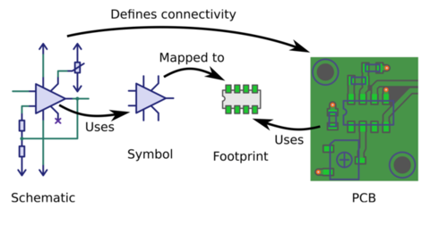
Step 1. Designing the circuit with Schematic Layout Editor using KI-Cad
Why to start with a schematic? The following excerpt is an interesting Pro-Tip from industry veterans.
An overview of the hi-level design stages in PCB manufacturing at scale:

“I start by determining the goal when creating the schematic. At minimum, some engineers understand the [goal of the] schematic to get to a netlist—to essentially create the connectivity.
Without the netlist you cannot move forward to do an actual layout. But if one thinks like that, one could create a netlist in a text editor directly, right?
However, a netlist does not meet the requirement of ease of readability. So, secondarily I make sure the schematic I create will communicate my intent in a graphical form, such that it is readable, not just by me, but also by my peers.” - Theodor Iacob/Hitchhiker’s guide to PCB design
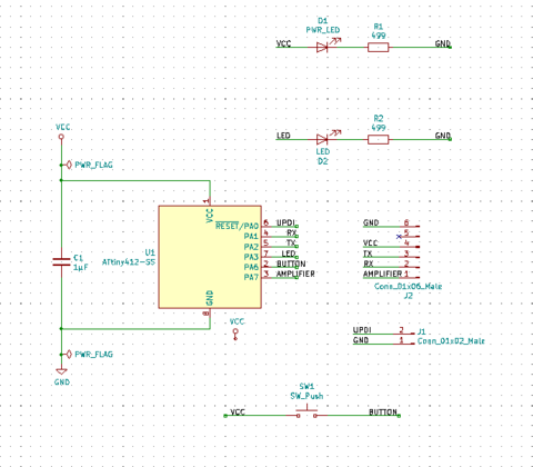
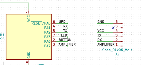
While modifying the new PCB blink board design as our circuit design, the basic reference diagram was the hello board design w/ the AtTiny412. Being new to the software, I followed the tutorial from the Aalto Fab Academy 2020 for the most part for modifying the board.
By using the library of symbols to design, starting with the microcontroller chip AtTiny412, one adds the necessary connections.
Step 2. Ki-Cad schematic Symbols - Usage and Creation
The electronics industry foresaw the issue of the need to standardized the layout schema many years ago and as a result, organizations such as ASME Y14.44-2008 and IEEE 315-1975 formed in order to standardize the way schematic symbols are depicted.
Ki-Cad libraries had a stock of these symbols existing in the library, which we will use to mark the different components. The “symbol editor” contains electronic language symbols according to the standards. One can also make one’s own symbols using this feature - however if it needs to be read in a collaborative effort (Which is almost always the case in industry or even hobby projects), then it is probably wise to adapt to the standard.
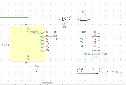
The Pin connections are appropriated according to the function needed. After adding the connections for the FTDI board(pins PA1 & PA2), and the 2 pin UPDI programmer(pin PA0) I added a “ghost pin” for PA7 for an output to send a signal apart from a programmable LED and button(Switch) to PA3 & PA7.
For each part, there is a separate documentation and technical details that can be checked in advance.
Once the schematic is designed, one can assign IDs for the components with the “annotate schematic” function. Finally, one can run the “rules check” bugs editor to check if everything is ok with our diagram, and there are no problematic connections.
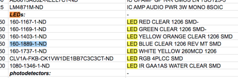
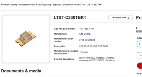
As an example, the LED used for the schematic, was traced first to the FabLab inventory.
This is because the inventory related to the library and the kind of documentation within fablab that supports the part.
Addition of the Power Status and Programmable LED.
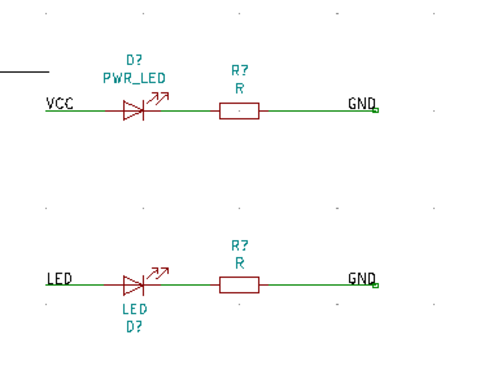
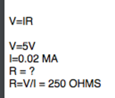
The power LED was added as a status check, useful to determine if the basic current flows through or not - and the resistance for this was calculated after referring to the datasheet of the LED.
Step 3. Schematic Capture & Editing
The schematic follows the connections step by step - by importing the symbols for the parts from the symbol library - and making the required connections.
In this case no new symbols were created as the existing libraries were enough.
Prior to proceeeding to the FootPrint editor, if needed one can look at DIGI-KEY’s website to check what each part’s footprint looks with the help of datasheets.
Step 4. Create Footprints
“The steps for placing components onto a PCB layout are very similar to those which would be followed by a construction company designing a house or a city. Successful completion of either requires an investment of time and planning. PCB component footprints are like the bricks of a building—they must be strong and pure. They must be located near the site for easy access.”” - Hitchhiker’s Guide to PCB Design
Using the Ki-Cad footprint editor. the diameters and positions of pads and holes used to electrically and mechanically attach components can be edited here. Eg. the AtTiny412 has 8 hole footprint for the 8 legs of the microcontroller.
Using the Ki-Cad footprint editor, we can also create and add our own parts to the library - as well as find existing ones.
In case one needs to create their own footprints, they need to refer to the precise DataSheet of the part. In some cases such as that of surface mount components - one has to precisely measure the component width in order to create their own footprint - which is a tedious job on ki-cad.
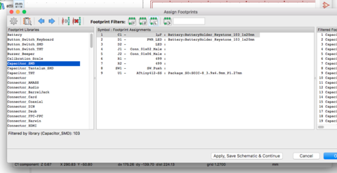
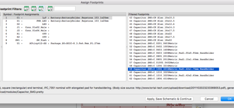
At this stage in the design, I can assign footprints using the existing FootPrint Libraries on the left panel - which gives a range of options for the selected component on the “filtered footprints” panel. For instance, via the footprint library, for the same component one can choose whether to choose footprint for SMD(surface mounted) or THL(through hole) components - in our case we choose SMD. And one can fine tune the choice in the filtered footprints depending on further details like style of soldering or component dimensions.
The pin connectors and switch were then designed as a new Project libraries - using existing template.
Eg. the Pin header with 2.54mm dimension was used as template and renamed and exported to local library.
The parameters were then edited according to the corresponding datasheets on Digi-Key. After editing the changes needed, it is uploaded to the footprint library as a custom entry for our local project.
update for 14 May 2020 - an immensely helpful Fablab footprint GIT library has been created here
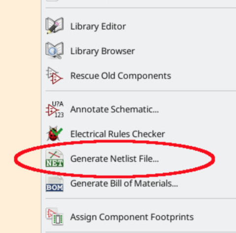
Step 5. Generate netlist
In order to match the Schematic symbols with footprints, we need to generate a metadata file about the interconnections - showing which schematics are connected with which symbols - this generated file is then reimported within the PCB board editing panel.
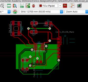
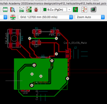
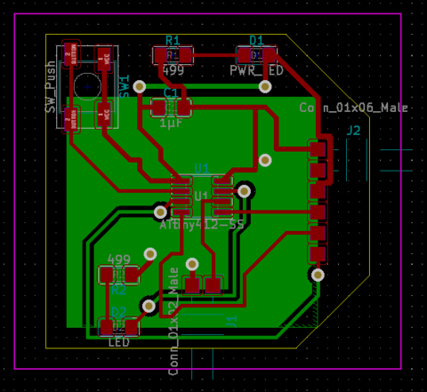
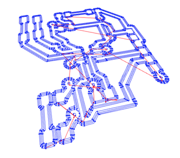
Step 6. PCB editing & Board Layout - aka Parts Placement
” When the component footprints are imported, they are automatically connected by fine lines to show their pin’s connectivity with other component pins. All these connections are based upon the previously established connectivity de ned in the schematic.
The imported part footprints usually appear to be piled up randomly off to the side of the de ned PCB outline after being imported into database.
A design with hundreds of components imported in this way will have so many connections crossed over one another, it will make the pile of parts and connections look like a rat’s nest (which is what it is often called).
To a new designer, this state of confusion can appear rather hopeless, but this is where the fun begins. This is the stage in which the designer can begin adding organization to what appears to be chaos.
Most designers consider the placement stage of layout their reason for being—they know this rest layout step will drive the success of the entire project because parts placement effects every manufacturing process and therefore every manufacturing stakeholder.”
- Hitchhiker’s guide to PCB design
This stage is where the design rules are set by the PCB manufacturer. The net list places the parts in place connected by thin connection “hint lines” - and we use the widgets to move the parts around as well as draw the traces and connections between necessary pins - ie nothing is connected until we make the connections actively.
Because this was my first HelloBoard and PCB design exercise, I had great difficulty fitting all the components onto the same board. As a result with the help of rivets, I created through holes in the board for connections between some of the modules on the reveres side of the PCB.
At this stage, the pre-defined size of the track width and other parameters such as drill thickness is adjusted, using Net Classes - such as in the case of, Net Class traces are customized separately for a double sided PCB board for 2 sided PCB rivets; as well as for classes such as VCC & Ground.
After this, the traces are connected between the respective components. The traces on the front side of the board are red & the backtraces (via) are in green, with the ground plane in green.
Once the layout is ready, an outline is made around the PCB that defines the cutting area - I experimented with an asymmetric pattern. A 0 line thickness polygon in the user drawings layer is made to match the outline to fill the space.
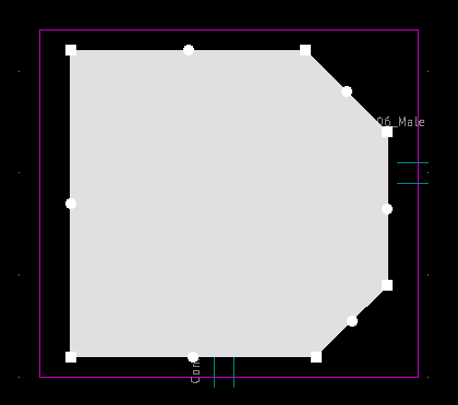
A margin is extended outside this polygon as an offset. Now that the board is ready, we export the front and back sides of the layout for the milling process.
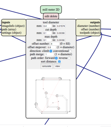
Step 7. Production and Milling
We now export the files that represent the layer of the board - The GerbView allows us to see the finished PCB layout.
The 4 files we need to generate are the front facing traces, the outline to be cut, the backtraces and finally the drill holes that go from the front of copper layer to the back.
These are exported as front trace and back trace and edge cut files from ki-cad as SVG format.
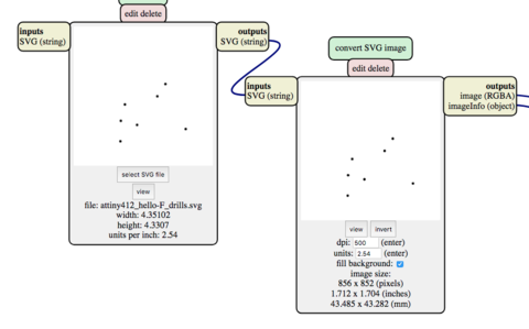
The formats exported are imported to image editing software specifically to isolate the rivet holes - in this case there are six rivet drill holes that need to be clearly depicted on the board in order to be traced out - and then need to be drilled through manually.
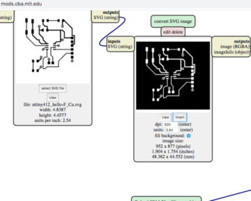
Generating the front traces using MODS
Generating the traces for the reverse side
ensuring all the drill holes are visible in mods for cutting
Generating the edge cuts
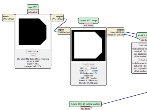
Generating traces for the milling
Milling the board
In order to mill the board, the Roland MDX 40 was used. As we are using a double sided board - there was a unique problem.
A double sided board needs to be flipped and put into the same slot on the reverse side where it was taken out from. This is because the X,Y settings need to be the same in order for the reverse side to have the exact counterpart on the other side - since we are building a tunnel through the board to connect components on opposite sides to a mm level precision.
My board was asymmetric in shape (on purpose, funky design) and that meant that once flipped, it would not fit into the previous slot.
The problem was thankfully solved by timely intervention by the FabLab master with a handy chiselling of the groove to somehow fit it into the same position. And it worked!
Here is the milled PCB board.
reverse side
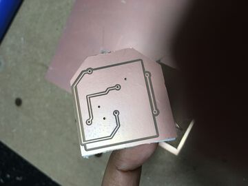
front side
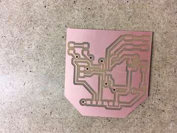
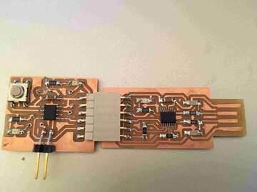
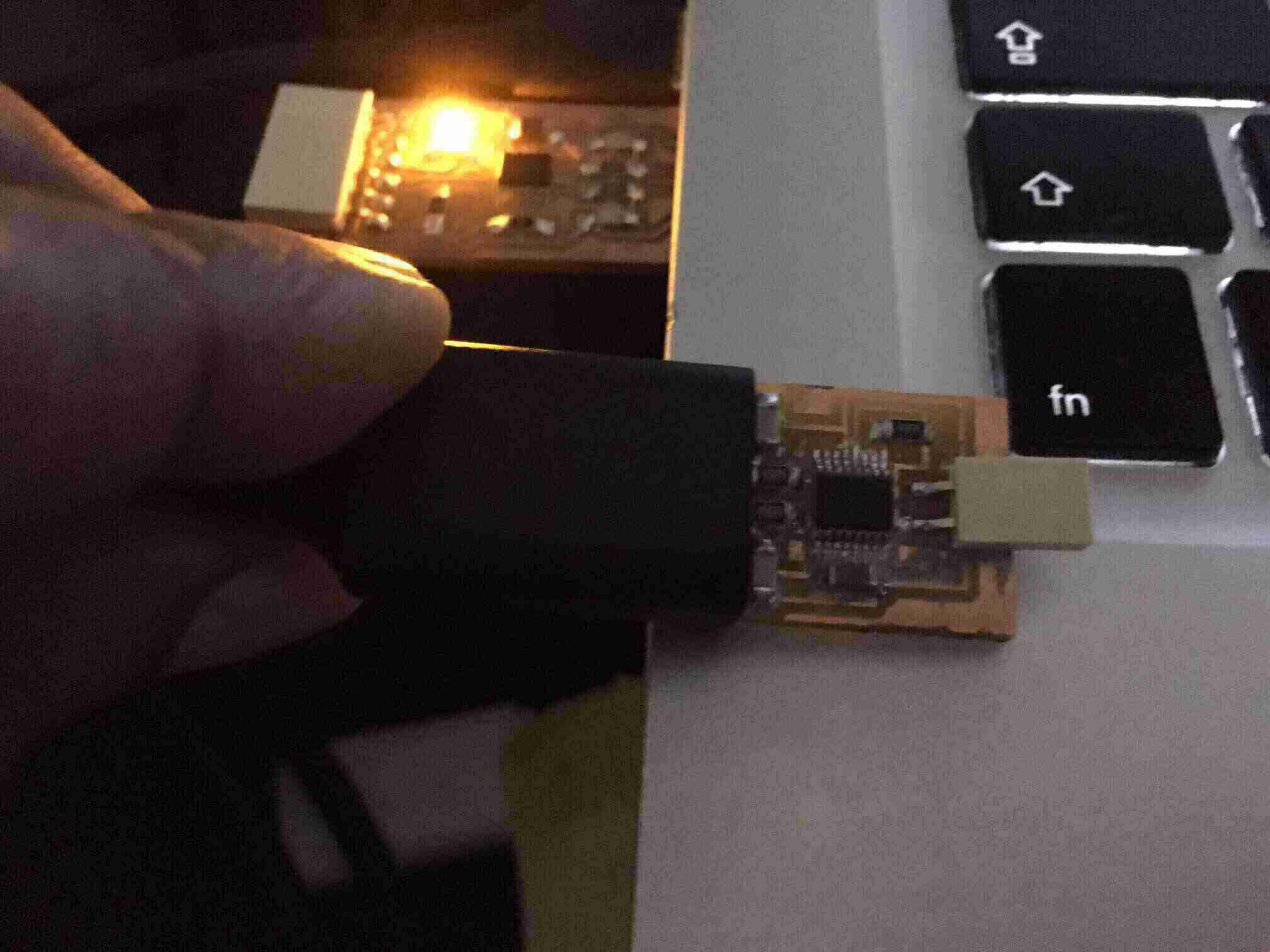
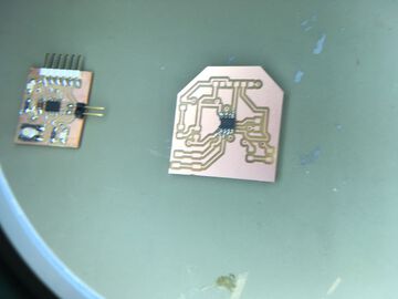
A comparison between the lab donated AtTiny 412 hello board and my AtTiny 412 hello board
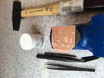
Step 8. Soldering & Testing
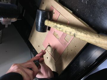
The first step was to drill through the marked drill hole traces, using 0.6 mm drillbit as seen below:
The next step was to hammer in the 0.6mm rivets in place to establish a “through hole” connection from the front end of the copper board to the reverse end.
Here some old crafstmanship tools came in handly.
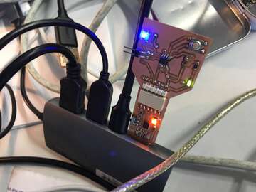
The components were then soldered onto the board and tested - it seemed to work!
files: download