Week's Assignments
Group Assignment:
● Use the test equipment in your lab to observe the operation of a microcontroller circuit board.
Individual Assignments:
● Redraw the echo hello-world board.
● Add (at least) a button and LED (with current-limiting resistor).
● Check the design rules, fabricate it, and test it.
Schematic and Layout
I decided to use Eagle as the PCB design software for my FabAcademy project.
Antti Mäntyniemi gave us a lecture
about the basic rules of PCB design and assisted us in getting started with Eagle. In addition, I watched some
Eagle tutorials on YouTube.
After installing Eagle, we needed to add the FabLab components
library to it. To accomplish this, I downloaded the eagle_fab.lbr,
and put it in the "library" folder of my Eagle.
(or you can put it anywhere in your computer and from Options > Directories (Fig. 1) define where Eagle looks for it).
To activate the library, select it from the left
menu, right click on it and check the 'use' box (Fig. 2).
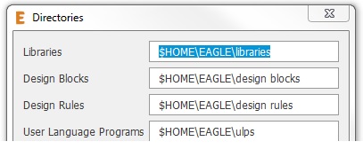 Figure 1.
 Defining library path.
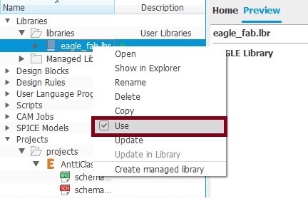 Figure 2.
 Activating the library.
For this week, we reverse-engineered an
an existing board
(echo board designed by Neil), and added a button
and a LED to it. Here is a summary of the steps that I followed to draw the schematic and layout:
Schematic
1. Creating a new project in Eagle from File > New > Project.
2. To Create a new Schematic (.sch), right click on your project in the left menu, then New > Schematic.
3. Adding the components needed from eagle_fab library, with Add Part tool (Fig. 3).
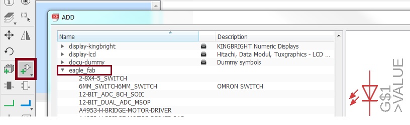 Figure 3.
 Adding the components.
4. To add a value to each component, right click on it and select Value.
5. Adding GND and VCC from supply1 library with the Add Part tool.
6. Wiring the components with the Net tool.
7. Check the correctness of the schematic by Electric Rule Check (ERC) (from the left menu).
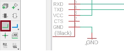 Figure 4.
 The Net tool.
Figure 5 shows the final view of my schematic. As can be seen, a simple RC low pass filter is added and connected to the push button as a de-bouncer circuit
(thanks to Antti for the suggestion).
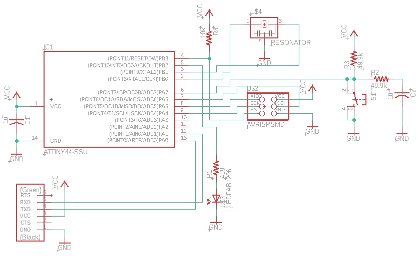 Figure 5.
 Schematic of my board.
Layout
8. Go to board editor by clicking on Generate/Switch to board icon (Fig. 6).
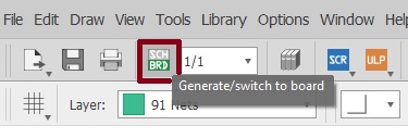 Figure 6.
 Switch to board editor.
9. Click on Move icon in the left menu to move the components to their place, so that you can minimize the wire length.
10. Define the Design Rules Check (DRC) parameters (e.g. minimum clearance) from Tools > DRC... (Fig. 7).
The minimum clearance cannot
be less that the diameter of the milling bit that you plan to use.
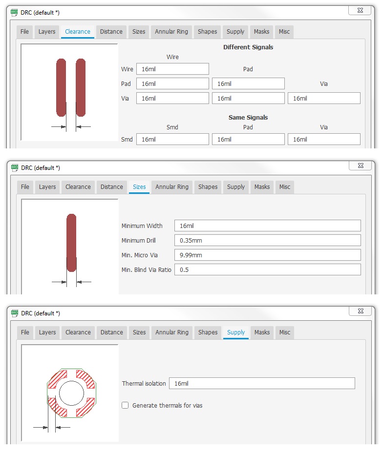 Figure 7.
 Defining Design Rules Check (DRC) parameters.
11. Set the Wires' width to 16mil and connect the component with the Route tools from left menu.
Make sure that you are working on the Top layer (Fig. 8).
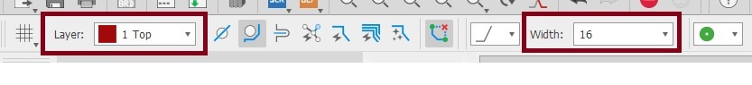 Figure 8.
 Setting the working layer and wire width.
12. When the routes between the components are ready, modify the size of the board. The board area is defined by the dimension layer (layer 20).
Simply
drag it to change it to your desired size.
13. To make the ground fills, follow these steps:
- In the top menu bar, make sure the top layer is selected.
- Click on the polygon icon in the left menu.
- Route the polygon in the shape you want it. Make sure to close it at the starting point. A polygon with a dashed line will appear.
- To connect the polygon to ground, right click on the dash line and select Name. Name the polygon GND (Fig. 9).
- Click on Ratsnest icon in the left menu.
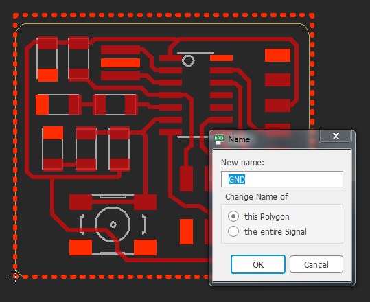 Figure 9.
 Connect the polygon to the ground.
14. To draw the outlines for cutting, set the working layer to Milling (layer 46),
and draw the the outline with Line tool from the left menu.
Outlines must be thicker than the diameter of the milling tool that you are going to use for cutting the outlines.
Since I was going to use a 1mm milling bit, I set the outlines width to 40mil (=1.016mm).
Figure 10 shows the final view of my PCB layout.
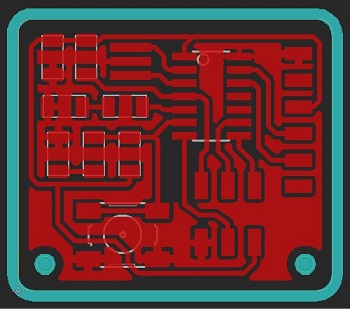 Figure 10.
 PCB layout of my board.
Fabricating the Board
I exported the designed PCB layout as black and white image files. Then, I used fabmodules To create an .rml file
for milling the board.
To export the traces:
- Set the background to black from option > User interface... > Layout > Background.
- Hide all the layers except the Top layer from View > Layer settings... (Fig. 11).
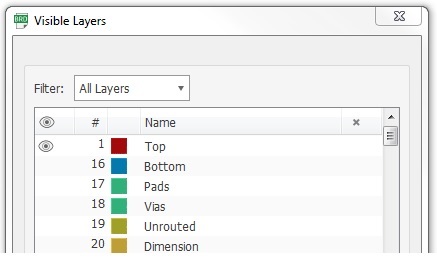 Figure 11.
 Layer setting for exporting the traces as an image.
- Go to File > Export > Image.
- Set the resolution to 2400dpi and select the monochrome (Fig. 12).
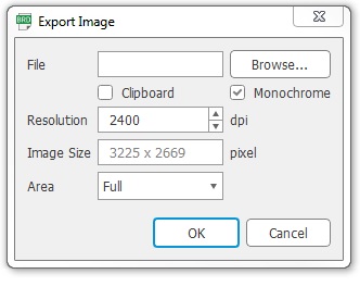 Figure 12.
 Image Setting.
To export the outlines:
The process for exporting the outlines as a .png file is roughly the same as traces.
But, you must set background to white, and only make the Milling layer (layer 46) visible.
Fig. 13 shows the exported images.
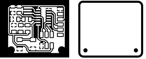 Figure 13.
 Traces and outline exported as .png files.
I used fabmodules to create the .rml file for milling machine.
I set the tool diameter to 0.2mm and cutting depth to 0.1mm (Fig. 14).
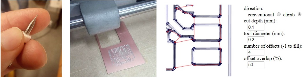 Figure 14.
 Milling the traces.
Similar to
week 4, before soldering the components on the board,
I cleaned the surface of the board using steel wool and robbing alcohol. The needed components were:
● 1x ATtiny45
● 1x 2x3 Pin header
● 1x 1x6 Pin header
● 1x 1uF Capacitor
● 1x 10nF Capacitor
● 1x 20MHz Oscillator
● 1x 499Ω Resistor
● 1x 10kΩ Resistor
● 2x 49.9Ω Resistors
● 1x Omron 6mm Push button
● 1x Blue LED
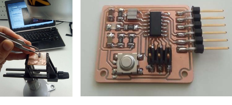
After soldering the components (Fig. 15), I did continuity testing with a multimeter, to make sure that all the connections are fine
and there is no unwanted shorts. For this purpose, set the multimeter to
diode mode.
Programming and Testing
Programming the Board:
Everything required for programming the microcontroller was already installed from
week 4.
I also used the ISP programmer that I made in week 4. This programmer does not
provide
VCC, so I powered the echo board through FTDI cable (Fig. 16).
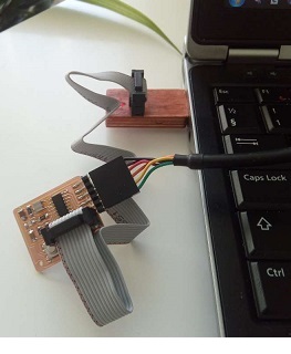 Figure 16.
 Programming the board using ISP programmer.
I downloaded the files below and saved them in the same directory:
●
hello.ftdi.44.echo.c
●
hello.ftdi.44.echo.c.make
Then, I opened a Git Bash and navigated to the folder with the downloaded files, and ran these commands to program the microcontroller:
- Running this command to compile the .c file and build the
.hex file:
make -f hello.ftdi.44.echo.c.make
- Set lfuse to 0x5E for 20 MHz external oscillator using this command:
make -f hello.ftdi.44.echo.c.make program-usbtiny-fuses
- Running the following command to program echo board microcontroller flash memory with the contents of the .hex file (Fig. 17).
make -f hello.ftdi.44.echo.c.make program-usbtiny
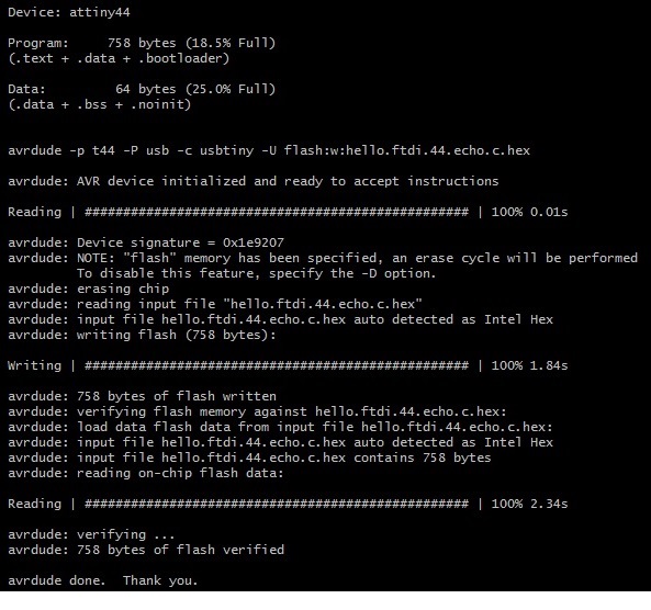 Figure 17.
 Successful programming of the microcontroller.
Testing the Board:
I used both PUTTY
and Adruino IDE
to test the board. First, I connected the echo board to a USB port via FTDI cable,
and checked the assigned serial port number from Control Panel > System > Device Manager (Fig. 18).
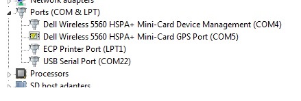 Figure 18.
 Check the assigned serial port number.
Then, I opened PUTTY terminal and set a session for serial, set Serial line to COM22 and Speed (Baud rate) to 115200 (Fig. 19).
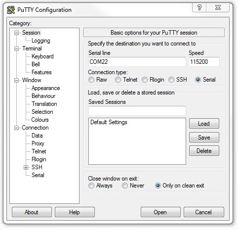 Figure 19.
 Set a session for serial in PUTTY.
The hello program that we burned on the microcontroller was a echo program. So if everything works fine,
it must return an echo of what we are writing in the PUTTY command prompt (Fig. 20).
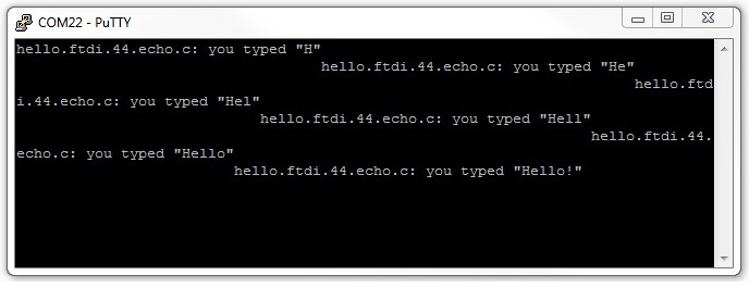 Figure 20.
 Returning echo of the pressed keys.
I also tested the board using Arduino IDE. First, I opened Arduino IDE.
Next, I selected the serial port assigned to echo board from Tools > Port. Then, I opened a
serial terminal from Tools > Serial Monitor. Finally, I set the the baud rate to 115200 (Fig. 21).
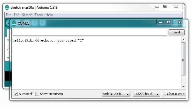 Figure 21.
 Testing the board using Arduino serial monitor.
Group Work
I had This week’s group assignment was to use the test equipment in the lab to observe the operation of a microcontroller circuit board. I did the task on my own this week.
I used Neil’s code for the individual assignment,
but I wrote my own sample code for the group work.
My sample code has a baud rate of 9600 (not the same as Neil’s code). A snapshot of the code that I wrote for the Group Work is shown in Fig. 22.
The test equipment that I used was a Tektronix MSO 2002B Mixed Signal Oscilloscope, which is capable of 200MHz bandwidth and 1 GS/s sample rate.
The device is shown in Fig 22.
The ‘Single’ button shows the result of a single measurement (without averaging many).
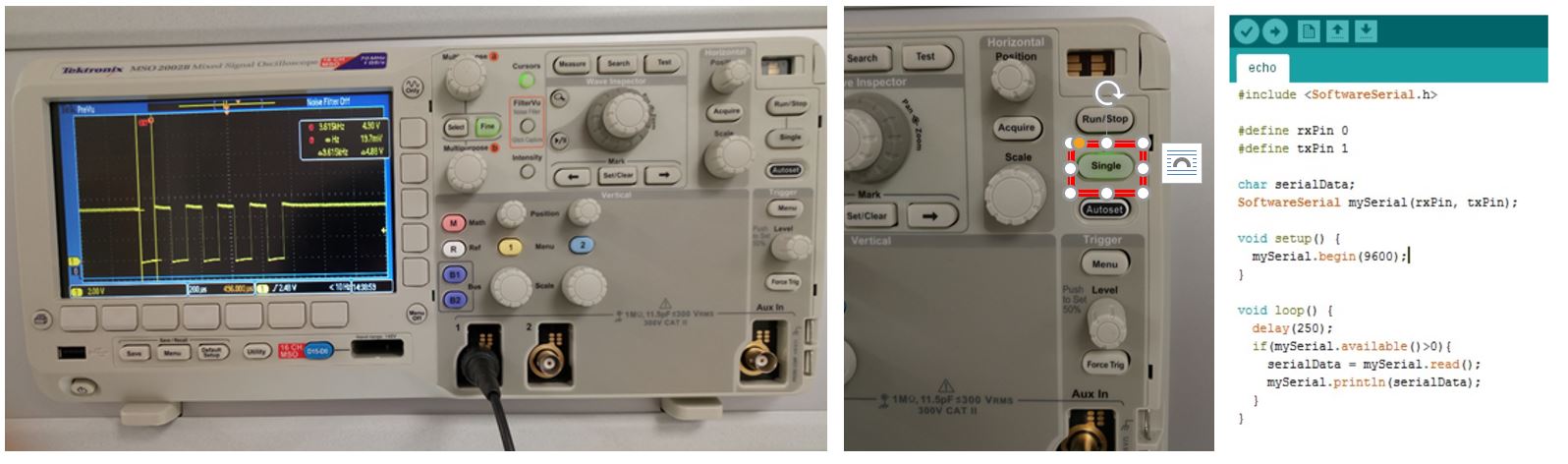 Figure 22.
 Tektronix MSO 2002B Mixed Signal Oscilloscope and group work code.
I used a passive probe in the measurements. First, I checked the baud rate with the scope.
Figure 23 shows the signal for transmitting "U" and the baud rate measurement result. Baud rate measured using oscilloscope was 9.615kHz,
that was close to the configured serial baud rate (9600).
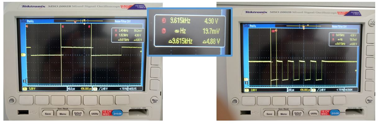 Figure 23.
 Baud rate check.
I used Arduino 'Serial Monitor' to send serial data. I typed in the characters ‘U’, ‘5’, '0' and ‘a’ and observed the the ASCII code for them in the serial format.
Figure 24 shows the data format when sent serially. According the data format, the order of the bits are a zero start bit, the 8 bit data form LSB to MSB and a one stop bit.
For example, binary code for “U” 01010101. The reading on the oscilloscope should be (from right to left) 0>1>0>1>0>1>0>1>0>1 (Fig. 23).
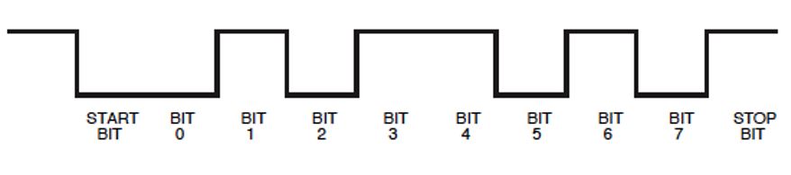 Figure 24.
 Serial data format.
Figure 25 shows each of the characters ‘0’, '5' and ‘a’ as seen on the oscilloscope.
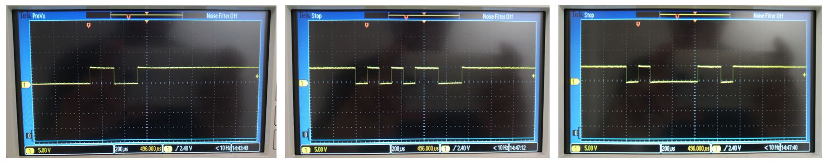 Figure 25.
 ASCII code serial test.
Reflection
I had designed several PCBs using KiCad and Eagle. But, it had been a long time that I used Eagle. This week's assignment was a useful practice for me to be confident
in using Eagle again. Also, I learned several valuable tips from Antti, for example he proposed a good
online calculator, to calibrate 'Depth of cut' and 'With of cut'
for the 'V' shape milling bits.