Week's Assignments
● Characterizing the design rules for PCB production process.
● Making an in-circuit programmer by milling the PCB.
● Soldering the components on the PCB and programming the microcontroller.
PCB Milling Process
Among the programmers suggested in the Fab Academy lecture page
for this week, I selected Brian’s version . He
documented the process very well. Besides, most of the former Fab Academy students from FabLab Oulu had done the same. Therefore, I could get good support,
if I would have faced a problem.
The .png files needed for PCB traces and cutout borders were provided by Brian in his page. Therefore, I just needed to make the .rmf file for the SRM-20 milling machine.
Making the .rml file:
Jari Pakarinen (Fab Lab Oulu staff and Fab Academy 2017 graduate) gave a comprehensive lecture on the subject, including how to convert the .png files to .rml using mods and fabmodules, SRM-20 machine, etc.
1. Go to fabmodules.org.
2. Select the .png file for the traces from input format > image (.png). Check the dpi and size of the image to make sure everything is all right.
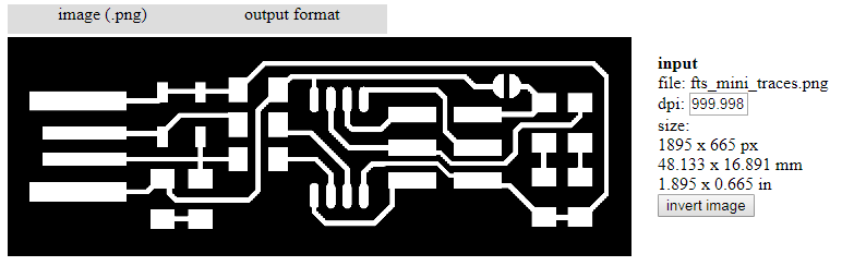
Figure 1. Importing the .png file to fabmodules
3. Select the .rml as the output format from output format > Roland mill (.rml).
4. Select the process from process > PCB traces (1/64).
5. Select SRM-20 as the milling machine. Set the speed to 4mm/s and origin (x0, y0, z0) to zero (Figure 2).
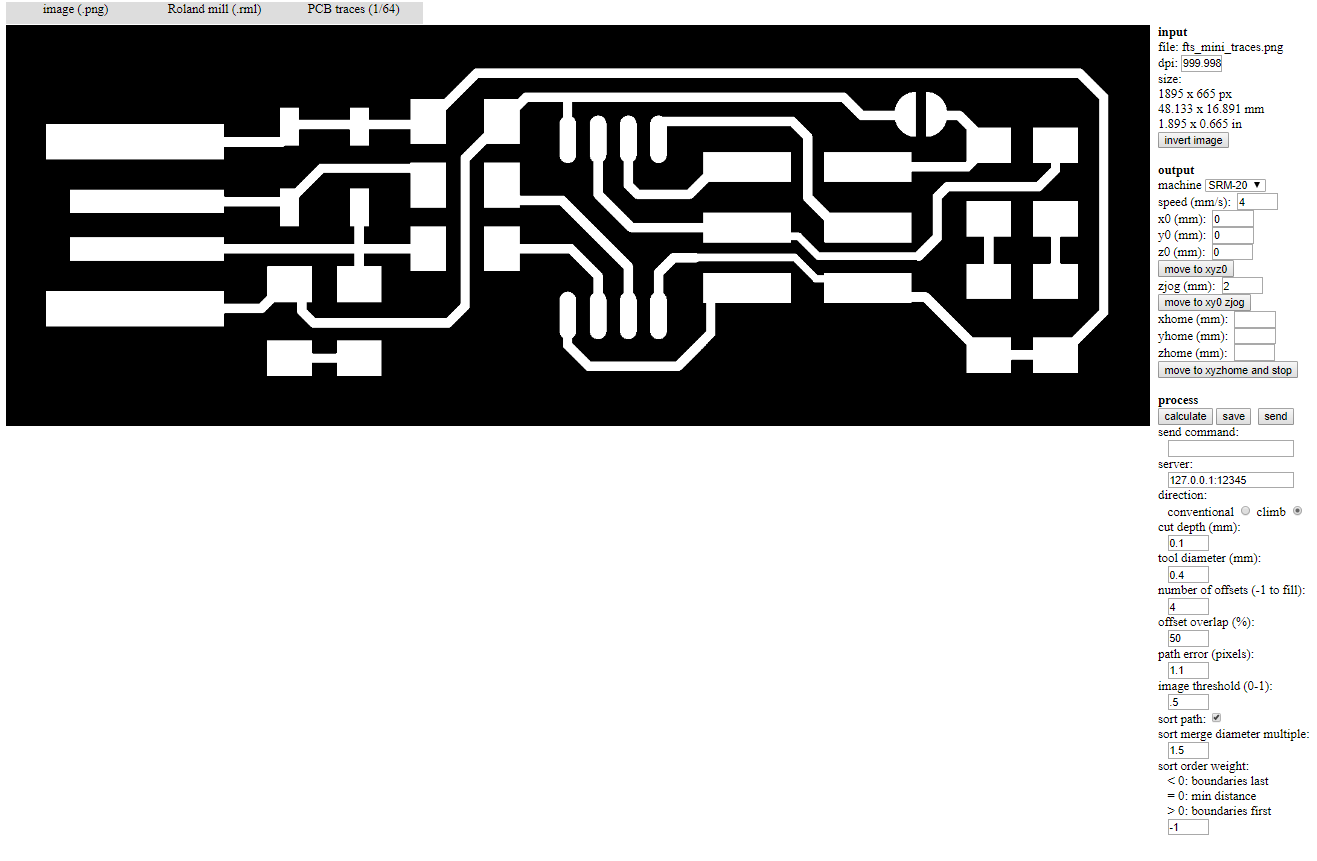
Figure 2. Machine settings.
6. Set the tool diameter (I used a 0.4mm flat milling tool).
7. Set the cut depth to 0.1mm. Since the FR-1 had a copper layer with a 35um thickness and I was using a flat milling bit, a 0.1mm cutting depth guaranteed
that the copper would be removed well (Figure 3).
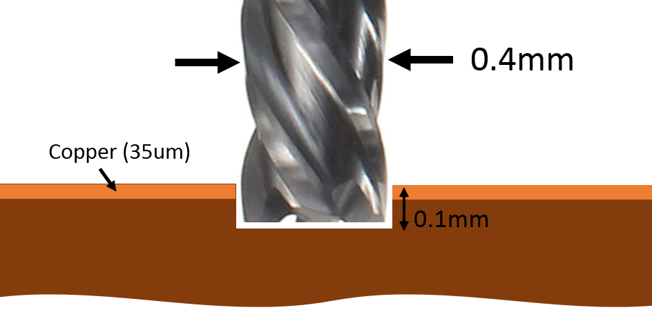
Figure 3. Setting the cut depth.
8. Set the number of clearance to 4 and offset overlap to 50%. Combined with the 0.4mm milling bit, which I was using, this settings provided a 0.8 mm trace clearance
(note that this is not the minimum trace clearance of the PCB) instead of removing all the black area on the .png file.
9. Press the calculate button (I got an output result similar to Figure 4). Now save the .rml file.
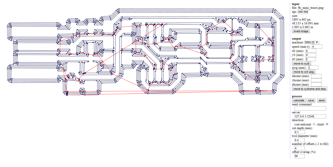
Figure 4. Calculated .rml file for the traces.
For producing the Cutout file, the process is more or less the same. After importing the cutout .png file and selecting .rml as the output, The process must be selected as PCB outline (1/32). For the cutting process, I used a 1mm flat milling bit, so the tool diameter was set to 1. Also, since the FR-1 board is roughly 1.7mm thick, I set the stock thickness to 1.7mm. The cut depth was set to 0.6mm, which means the milling bit accomplishes the cutting process within three rounds, cutting 0.6mm deep in each round. You can rotate the calculated output and see it from different angles by dragging the mouse while holding the right click button (Figure 5).
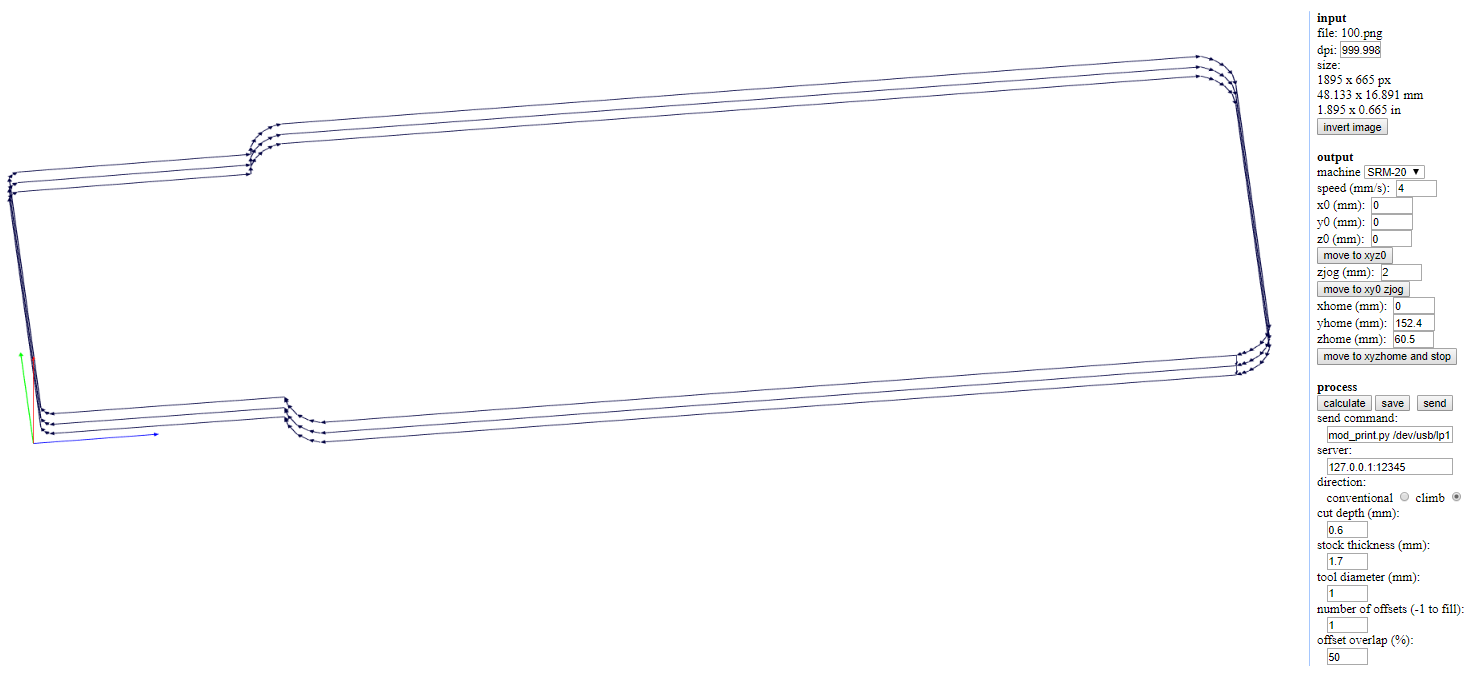
Figure 5. Calculated .rml file for the cutout.
Milling the PCB:
Fab Lab Oulu is equipped with two Roland SRM-20 compact milling machines.
They have 232mm by 156mm work piece tables with a 0.01mm resolution. A more detailed specification of the machines can be found here.
Fixing the FR-1 board in the milling machine and placing the milling bit:
The first thing to do is finding a piece of FR-1 board and fixing it on the workpiece table of the milling machine. The board Should not be bent, even a small curve in the board might ruin the milling process. If the size of the FR-1 board is much larger than the size of PCB, it is better to cut the board to a smaller piece. Figure 6 shows why the smaller piece is less bent. To fix the board in the milling machine, I used double-sided tape.
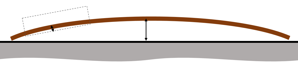
Figure 6. Fixing FR-1 boards of different sizes on the workpiece table.
In order to attach the milling bit, hold it between your fingers, as shown in Figure 7, and put it in its place. Then tighten it using a hex key tool.
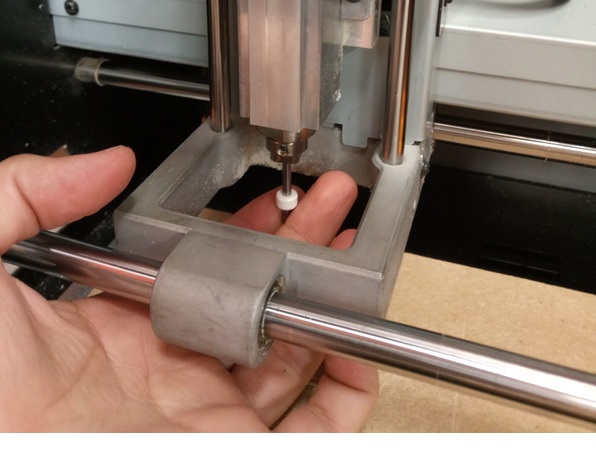
Figure 7. Installing the milling bit.
Settiong the origins:
Now turn on the milling machine (Power button is located on the top right side of the machine), and start the Vpanel for SRM-20 software. Table 1 explains the function of each section of the software. More details can be found here.
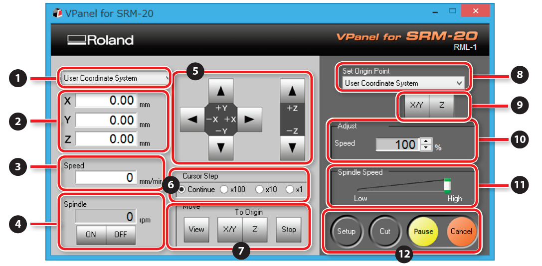
Figure 8. Vpanel for SRM-2.
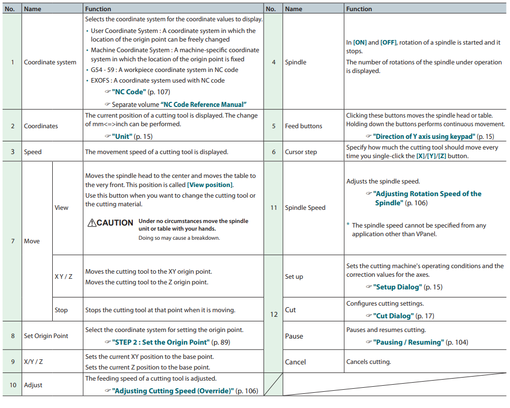
Table 1. Functions in the milling machine software.
To set the X/Y origin point, change the milling bit's position using the arrow buttons that are shown in section 5 of Figure 8. Speed of the movement can be set from section 6. When you reached to the desired position, press the X/Y button from section 9 to set the X/Y origin of the machine. Setting the origin for the Z axis is a little bit tricky. Move the milling bit close to the surface of the board using the arrow buttons for Z axis in section 5. Be careful that the milling bit does not touch the surface of the board (when it is getting close to the board decrease the speed). When the milling bit is roughly 1-2mm from the surface of the board, stop moving it. Now loosen the milling bit using a hex key tool and let the bit tool fall down to touch the copper surface of the board. Then re-tighten the mill bit and set the Z origin to the machine using Z button located in section 9. To start the milling process, first press the Cut button. Then click the Add button (Figure 9) and select the .rml file. Finally click the Output and let the machine does the job.
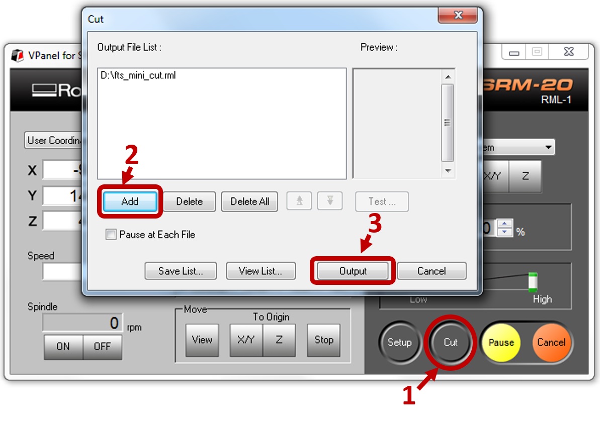
Figure 9. Starting Milling Process.
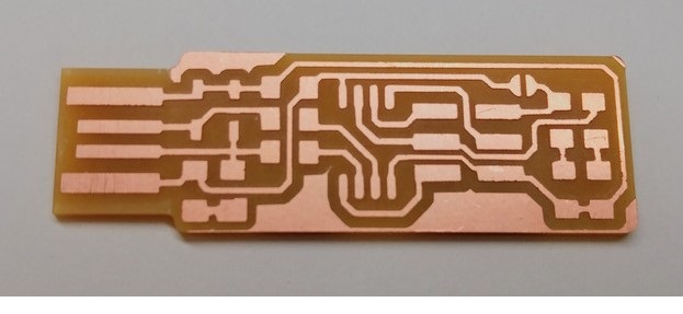
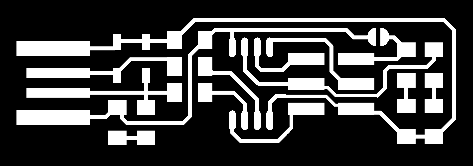
Figure 10. My programmer's PCB.
Soldering the Components
First I picked the SMD components that were needed for the programmer according to the Brian's instructions. Before starting the soldering, remember to peel off the extra coppers around the usb pins (unfortunately I forgot to take an image before doing it). But hopefully you can find it in Brian's instructions. For having a clean soldering, it is essential to make the PCB surface super clean. I washed the PCB board, then I scrub it using a piece of steel wool and washed it again. Finally I cleaned it using rubbing alcohol. Figure 10 shows my PCB with the components soldered on it.
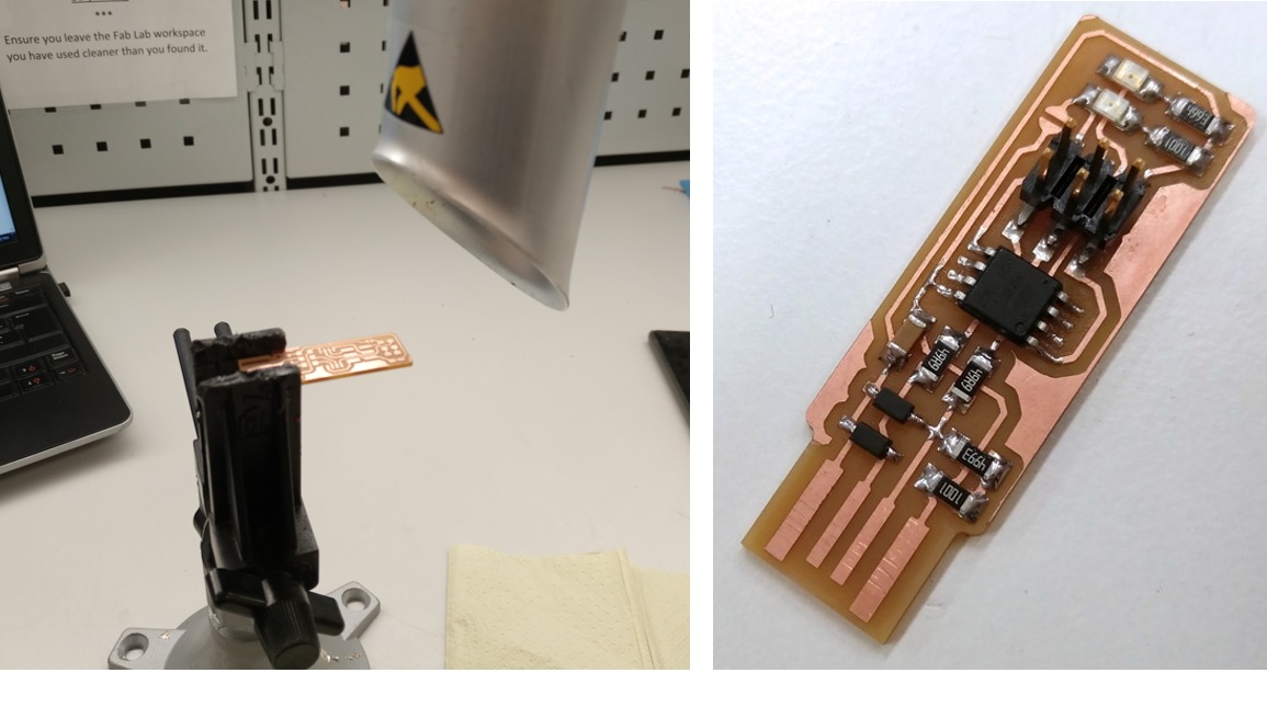
Figure 11. My PCB with soldered components.
Programming the ISP
Brian provided a detailed programming instruction , in Linux, Windows and MacOS operating systems. I performed the programming using Windows 7. Here's a brief explanation of the steps that I took:
1. Installing Atmel GNU Toolchain (The link provided by Brian did not work, But I could download it from here ).
2. Installing GNU Make.
3. Installing avrdude.
4. Updating the PATH in Control Panel >System > Advanced System Settings > Environment Variables.
5. Installing Driver for the Programmer: Download Zadig. Plug in the programmer and select USBtinySPI device in the list.
Then select libusb-win32 as driver and click the Install Driver button (Figure 12).
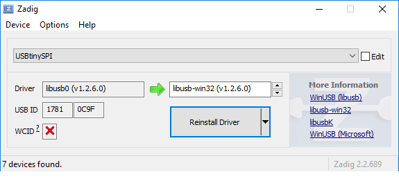
Figure 12. Installing Driver for the Programmer.
6. Downloading the firmware source code.
Then, I opened a Git Bash and navigated to the folder of the firmware source codes, and followed steps below to program the ATtiny45 microcontroller (soldered on my PCB). I used Jani's programmer (USBTiny) as the programmer. I connected my own programmer to Jani’s Programmer and the Jani’s to one of my laptop's usb port.
7. Making a solder bridge, in order to connect the existing jumper on the PCB.
8. Plug the USBTiny Programmer to a USB port (preferably USB 2.0). Then Connect the programmer to my board using ISP header cable. If everything is connected correctly, the red LED on the board should be lit up.
9. Running make command to build the .hex file.
10. Running make flash to erase the target chip, and program its flash memory with the contents of the .hex file (figure 13).
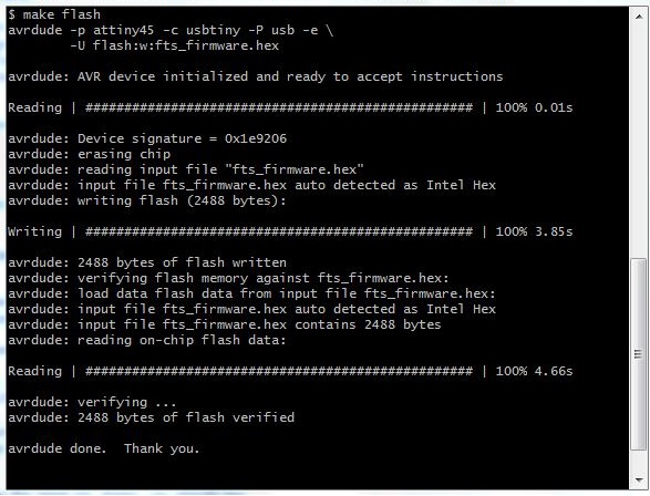
Figure 13. Programming ATtiny45 flash memory with the contents of the .hex file.
11. Running the make fuses command.
12. Running the make rstdisbl command.
13. Removing the bridge on the solder jumper.
I passed all the steps successfully and programmed the microcontroller, but windows did not recognize my board even as a connected device. After spending a few hours debugging, I finally managed to find the problem with the programmer board. The resistor between Zener diode and vcc was incorrect. I had picked a 499k ohm (4993) resistor instead of (4990) (Figure 14). I replaced the resistors with the correct ones, then I could find my programmer under Device Manager (Figure 15).
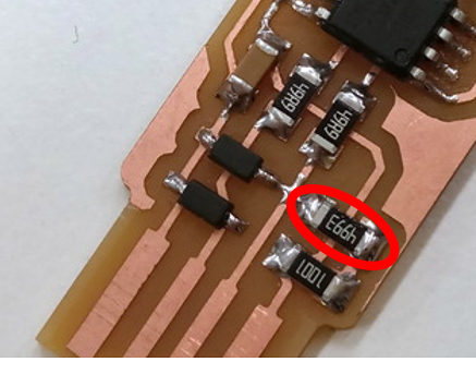
Figure 14. The 4990 resistor.
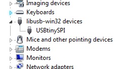
Figure 15..
Making a cover
I decided to make a wooden cover for my ISP programmer, using the SRM-20 milling machine. I almost accomplished the task with the same method that I used to build the pcb. I found two small pieces of 4mm thick pine wood in the Fab Lab to to use for making the cover. I made two .png files (by manipulating Brian’s .png file) as the Cutout files (Figure 16), to cut the two sides of the cover. However, I could have done the task simply using the laser cutter, but I did not want to have signs of burning in the edges of the cover.

Figure 16. Cutout images of the cover.
In order to make room for the programmer within the cover, I made a .png file (Figure 17) according to the size of the programmer pcb. The same as the previous step, I used the .png file to make an .rml file for milling machine.

Figure 17. Inside the cover.
I wanted to go 3mm deep on each side of the cover to make enough room for the programmer. The milling bit I used for this purpose was a 2.38mm flat type, also I selected the cutout process in fabmodules. The other important settings and calculated .rml file can be seen in (Figure 18).
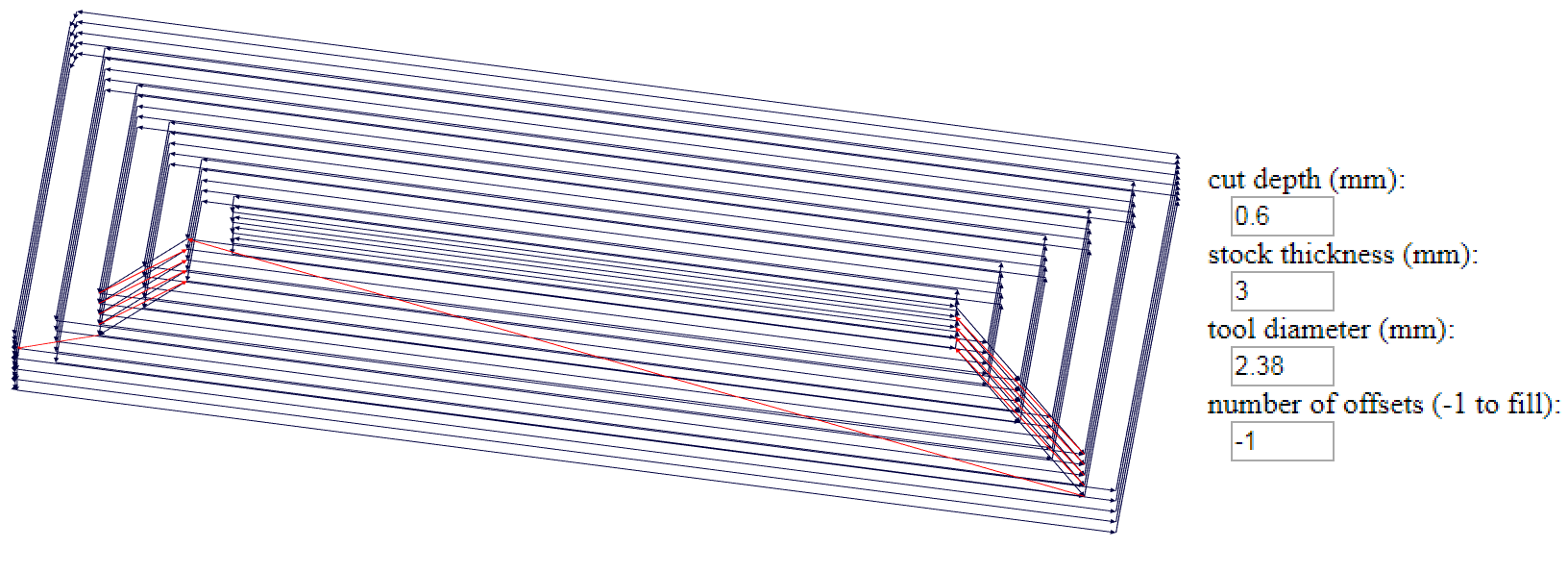
Figure 18. The .rml file for the cover.
I also removed the metal support of a broken usb cord and used it in my programmer.
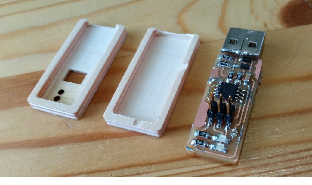
Figure 19. Programmer and its cover.
To make holes for the LEDs, I used the laser cutter machine in Fab Lab. In order to find the exact position of the LEDs on the cover, I made a .svg file using Inkscape (Figure 20). The green and red circles are for cutting and the rest is for engraving. I first engraved on a piece of pine wood, then I aligned the cover according on to engraving result. I used the same technique to engrave my name to the top side of the cover (Figure 21).
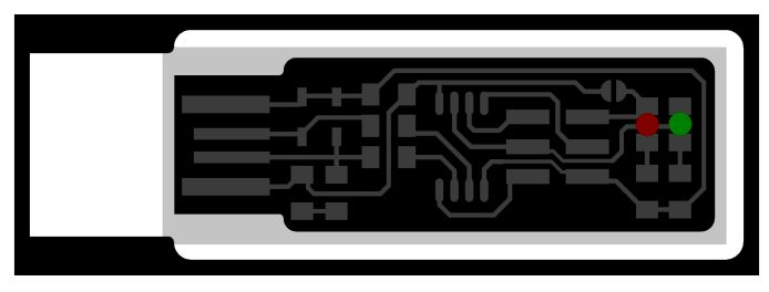
Figure 20. The Inkspace file for LED positions.
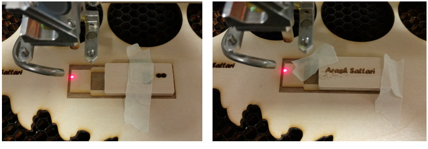
Figure 21. Engraving Process.
At the end, I applied a mixture of olive oil and brown polish shoe as a finish to the wooden cover. I also added a thin layer of clear coat for protection of the applied mixture. Figure 22 and 23 show the final result of this week's assignment.
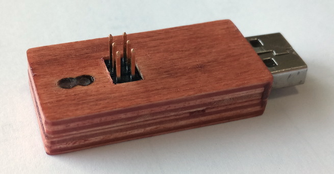
Figure 22. My programmer (bottom side).
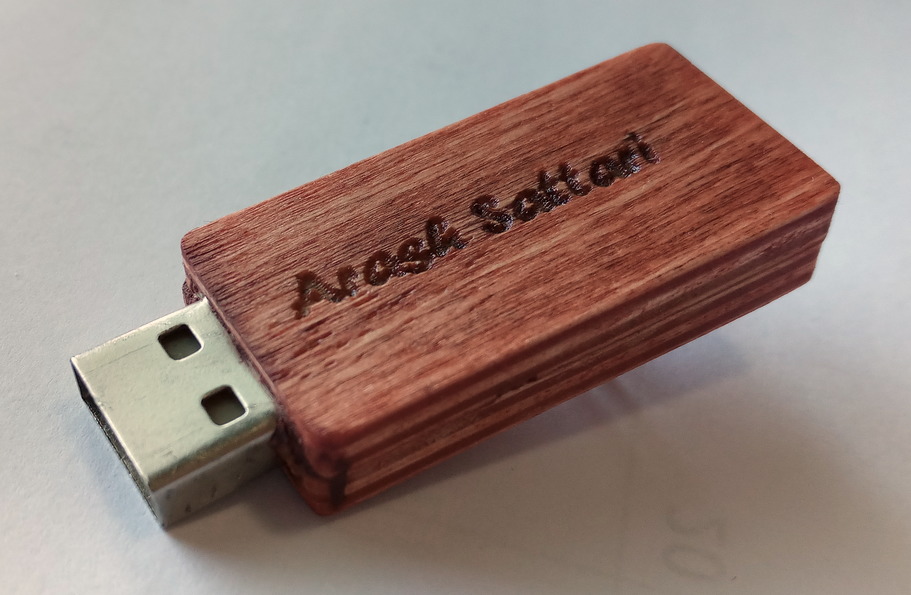
Figure 23. My programmer (top side).
Group Work
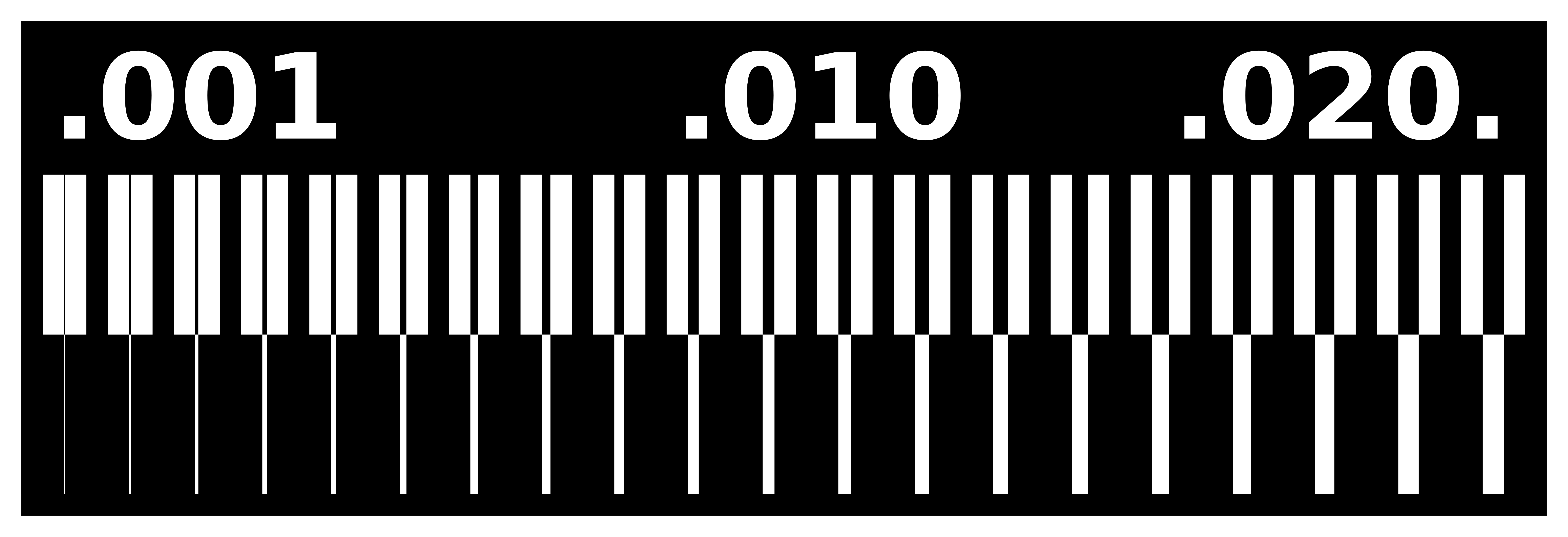
Alok, Michael and I worked as a group. In order to characterize the design rules for our PCB production process, we downloaded a .png file (Figure 24) and milled the pattern using different milling bits (0.4mm flat and 0.2-0.5mm V shape) and settings to investigate the milling results.

Figure 24. Desired traces that should be milled
For the group work we used mods to make the .rml files. The following procedure was done at mods to generate the required files:
1. Right click and select programs (Figure 25.1).
2. Select open server program (Figure 25.2), then choose Roland/mill/SRM-20/PCB (Figure 25.3).
3. After selecting Roland/mill/SRM-20/PCB, the default program will open which wants to communicate with the
Roland over sockets, but since in our case Roland is not connected to the same PC, so instead of sending the output to a socket we send it to a file. So as shown in figure x.y,
delete the websockets module, right click to add a new server module called file/save.
4. Connect the input port of file/save module to the output port of Roland SRM-20 milling machine output port.
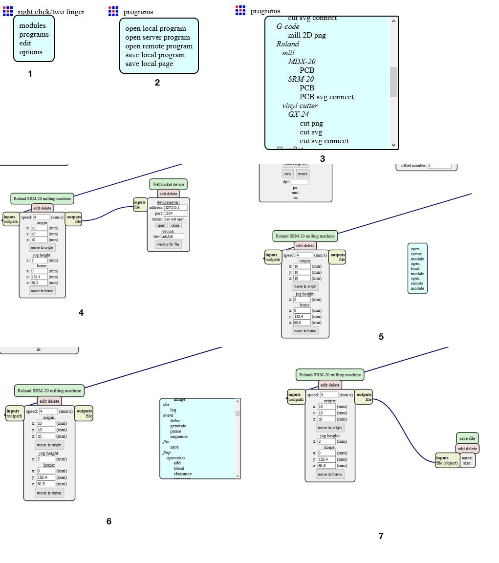
Figure 25. Steps taken to get the milling program in the mods
In the png file, the mill runs on the edge of the white, a bit on the black side and it takes away the black part of the png files. The recommended dpi for the png file is 1500.
The offset number tells the number of passes the tool makes and the offset step-over tells the overlap percentage.
In the picture below we have marked with red all the places where some change was done. In the top left corner, we had to put in the png file name. In the right corner we have the
tool settings. In the middle “mill traces” is selected as we are milling the traces and not cutting the outline. In the bottom left the origin is set to 0,0,0.
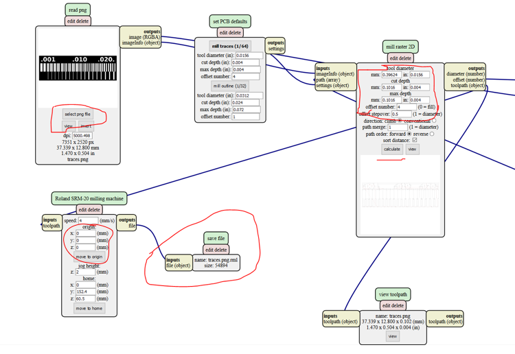
Figure 26. Steps taken to get the files needed for milling from the mods program
We used 3 different parameters (shown in the table below) for the milling bits. We first milled the PCB with a flat bit of diameter 0.4 mm with a cutting depth of 0.1 mmm. Then for the other two we defined the diameter settings in the software of the program. The results can be seen in table 2. The milling process (Figure 27) was as explained in PCB Milling Process section.
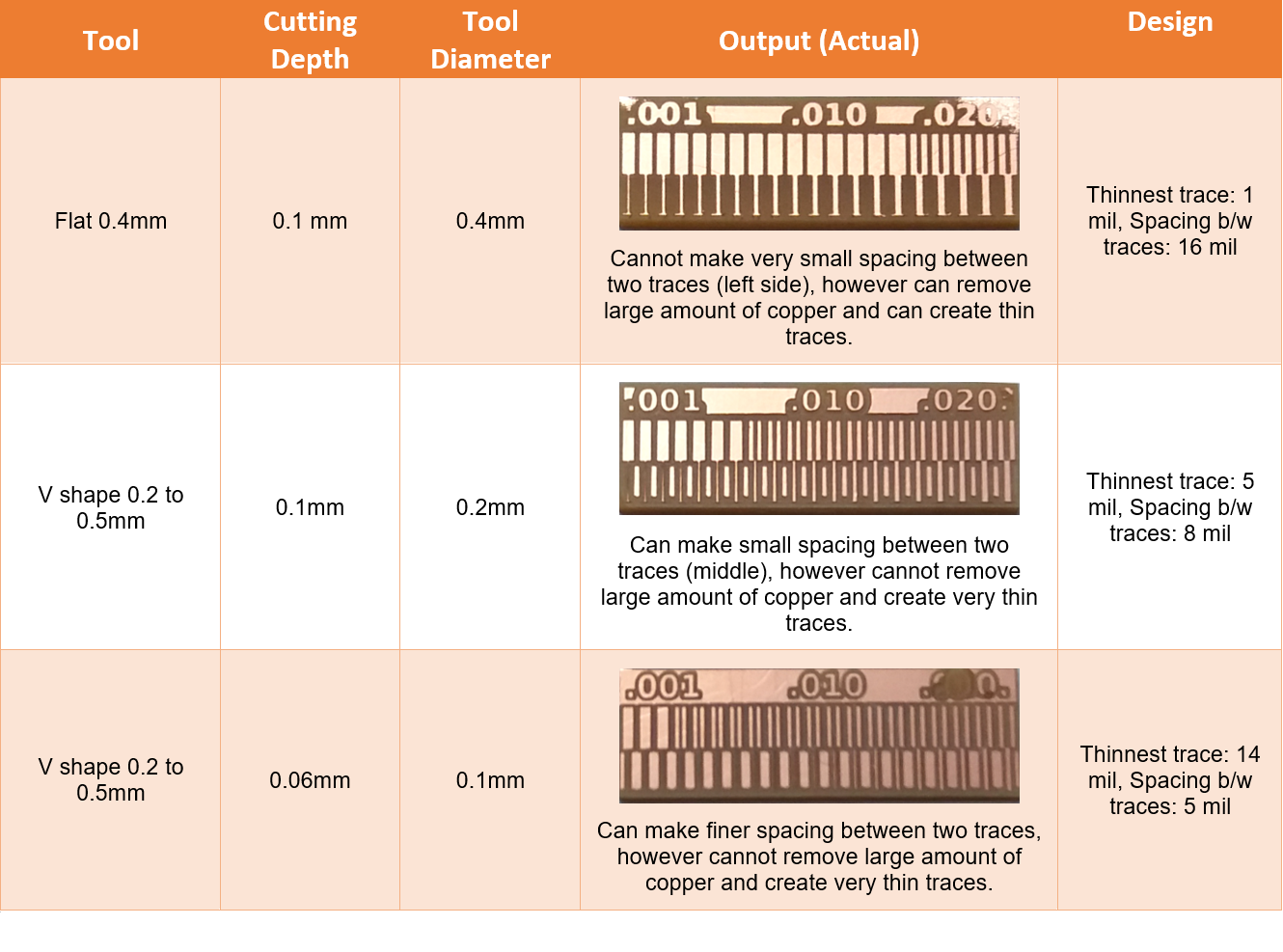
Table 2. Output Results
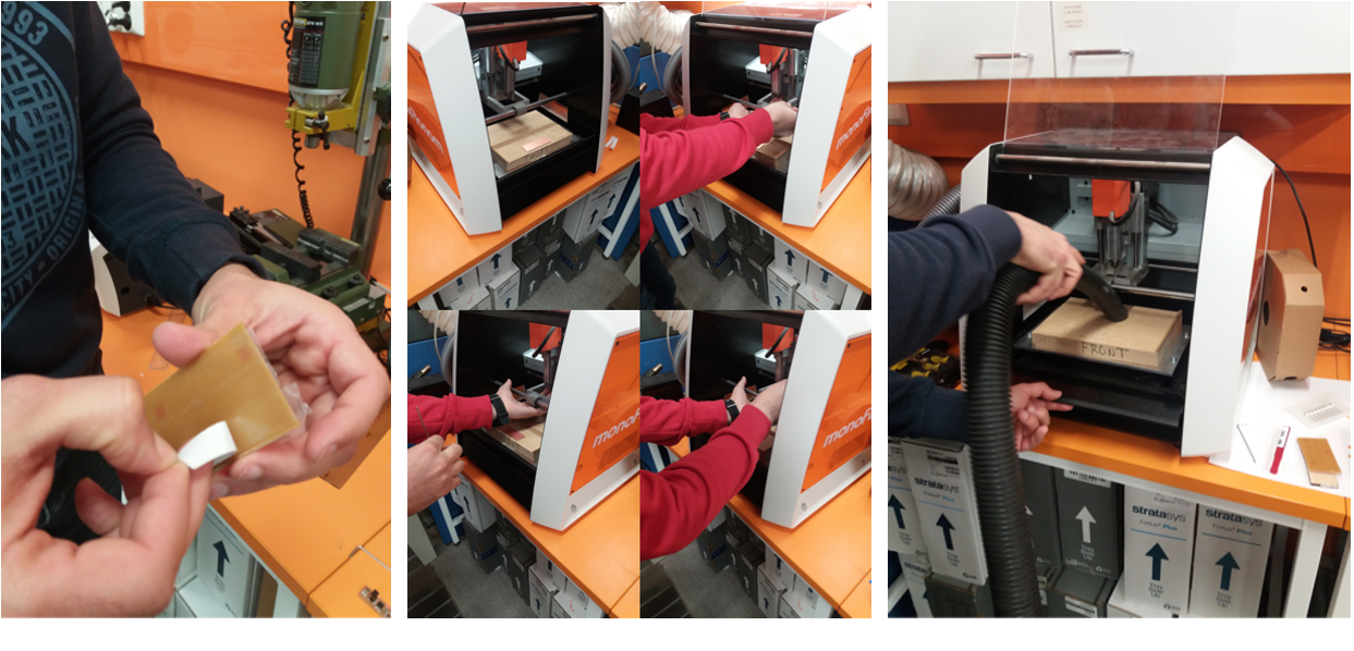
Figure 27. Milling the test board via SRM-20 milling machine.