Week's Assignments
Group Assignment:
● Probe an input device’s analog levels and digital signals.
Individual Assignments:
● Measure something: add a sensor to a microcontroller board that you have designed and read it.
Electronics Design
For the test board, I modified the electronics and PCB design of
Electronics Design's week.
Fig. 1 shows the schematics of the design. ATTiny44 (8-bit AVR Microcontroller) which has a 10-bit ADC.
As the input device,
I used a temperature sensor RTD 1kohm 1206, which will be explained in detail later in this report.
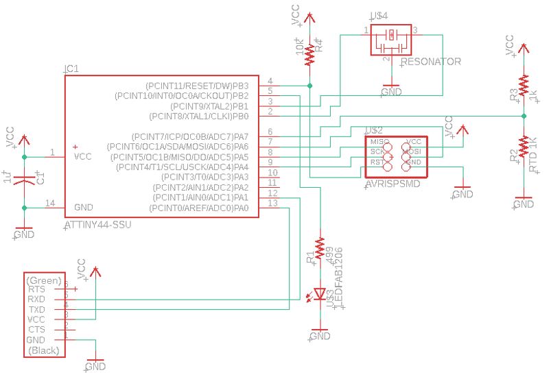 Figure 1.
 Schematic of the designed electronics.
PCB Design
When designing the PCB for the schematics of Fig. 1, I decided to experiment a new feature,
adding a logo to the PCB. I did a bit of research and found this useful video.
I followed the suggested steps, and added a FabLab logo to my design (Fig. 2):
1. Make a black and white version of the logo from the colored one (I used gimp for this).
2. Saved the image as a 16-color bitmap format.
3. Before starting floorplanning and wiring, place the image on the PCB.
4. Make all layers invisible except the one you want for the logo
(choose layer 22 bPlace, if you want the logo at the back side or layer 21 tPlace ,
if you want the logo at the front side. I had a one-sided PCB, so the choice was obvious!).
5. Go to File> Run ULP> select ‘import.bmp.ulp’.
6. Select the logo > open > choose no scan > select ‘black’ as the color >
specify the DPI and layer > click OK> Run script.
7. The logo appears on the screen with the logo file address.
8. To get rid of the address push Ctrl+z.
9. Since the graphic of the logo is made from many parallel lines, to move it,
select the group button > select all the lines > select the move button > press Crtl + right click >
drag the logo to wherever you want.
10. Make all layers visible again.
11. If the size does not fit your design, you cannot change it on the PCB layout
and must go all the way back to step 2,
change the image size before saving it and redo all the steps.
I used 0.2-0.5mm V-shape milling and followed a milling process similar to Electronics Design week.
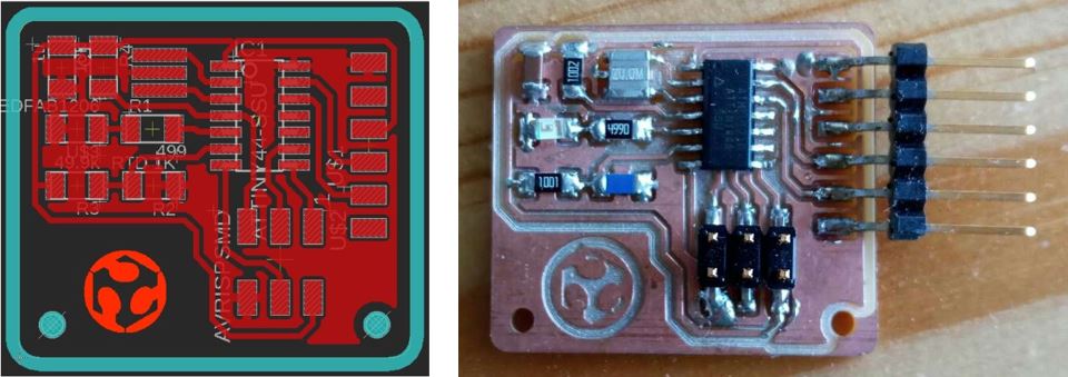 Figure 2.
 The PCB layout and fabricated board.
Sensor Measurement
As I mentioned, my input was a 1kohms temperature sensor.
This means that the resistance between the two pins of the sensor changes with temperature.
Fig. 3 shows the pattern of the resistance change vs. temperature.
R0 is the resistance of the sensor, when it is exposed to zero-degree temperature.
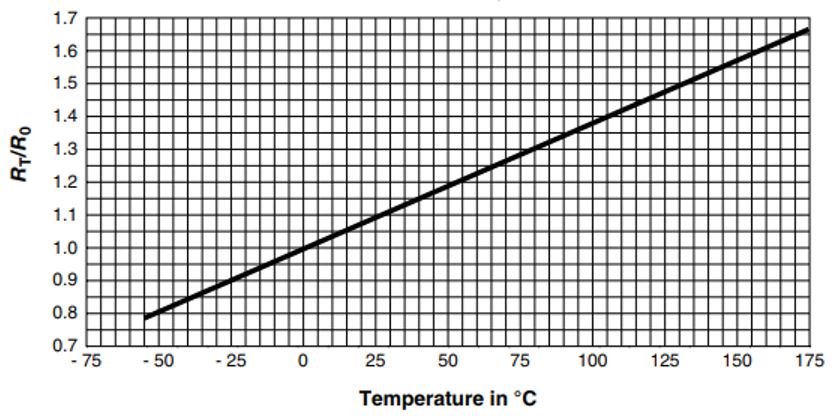 Figure 3.
 Resistance vs. temp.
According to the pattern: Rt = 1000 + 3.75T, in which Rt is the resistance when the sensor
measures T degrees. I biased the sensor in a resistor division with a 1kohm resistor
(R3 in the schematic) between
VDD (5V) and GND and connected it to the on-chip ADC of my microcontroller (right side of Fig. 1).
I wrote a simple code in Arduino IDE to test the sensor. The code is fairly simple,
it reads the value from the analog pin, which sensor is connected to. Then, it calculates
the actual temperature according to
the formula was mentioned above and sends it to the computer via serial communication. The programming process is described in details
in the Embedded Programming week.
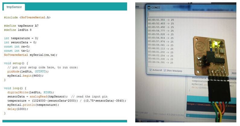 Figure 4.
 Code and result.
Group Work
I did the group assignment for this week on my own.
With the above-mentioned configuration, I was able to probe my input’s voltage level with
three different methods: at the pins of the sensor with a multimeter (analog),
after digital conversion with an oscilloscope (digital, Fig. 5) and the code result
of microcontroller (digital).
The multimeter showed 2.667V (Fig. 4). To interpret this, we have to remember
that the multimeter reading is RtR3/(Rt + R3) (according to the resistance division
equation). This means that with the above-mentioned reading,
the sensor’s resistance value, and its corresponding temperature are 1143ohm
and ~30 degrees, respectively.
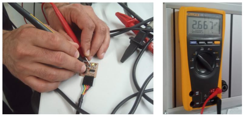 Figure 5.
 Probing with multimeter.
The code written for programming the ATTiny44 is shown in Figure 6. According to the ATTiny datasheet, it has eight 10-bit ADC channels on
the pins 6-13 covering 5V range (I connected the temperature sensor to pin 6 of the microcontroller). It means that the ADC result is Rt×1024/(Rt+R1). My code returns 29 as the analog to digital conversion.
The temperature readings were of course higher than the environment temperature due to the test board heating up during operation.
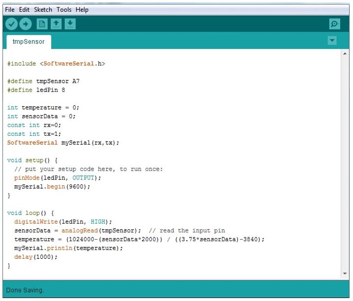 Figure 6.
 Measurement code.
Fig. 7 shows the bit stream of the result after the analog to digital conversion,
which is the same as what is read from the code result. The temperature variable is defined
as integer so the results is being sent in 4 bytes, the first two of which are the conversion result.
I got the following: 00110010, 00111001, 00001101, 0001010, which are ASCII code for 2, 9,
line feed and carriage return, respectively. So, the digital code represents 29 degrees.
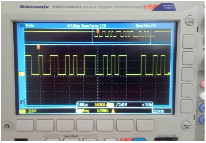 Figure 7.
 Probing with oscilloscope.
Reflection
I already had experience in working with input devices. However, this week I learned
how to add an image to a PCB design.