Week 14 : Assignment
- design, build and connect wired or wireless node(s) with network or bus addresses
Embedded systems Communication protocols
Analog
Simple sensors do not implement the conversion and communication logic, and the output is just the analog signal – voltage level depending on the value of the parameter that is measured. It needs to be further converted into a digital representation; this process can be made by analog to digital converters (ADC) implemented as the internal part of a microcontroller or separate integrated circuit. Examples of the sensors with analog output are a photoresistor, thermistor, potentiometer, resistive touchscreen. One can learn more about these terms in week 9 and Wiki
Digital
Dummy, true/false information can be processed via digital I/O. Most devices use positive logic, where, i.e. +5 V (TTL) or +3.3 V (those are the most popular, yet there do exist other voltage standards) presents a logical one, while 0V
presents logical zero. In real systems this bounding is fuzzy and brings some tolerance, simplifying, i.e. communication from 3.3 V output to 5 V input, without a need of the conversion (note, the reverse conversion is usually not so
straightforward, as 3.3 V inputs driven by 5V output may burn easily). A sample of the sensor providing binary data is a button (On/Off).Wiki
Click here to know the difference between Analog and Digital signals !
SPI
One of the most popular interfaces to connect the sensor is SPI (Serial Peripheral Interface). It is a synchronous serial interface and protocol that can transmit data with speed up to 20 Mbps. SPI is used to communicate microcontrollers with one or more peripheral devices over short distances – usually internally in the device. In SPI connection there is always one master device, in most cases, the microcontroller (μC) controls the transmission, and one or more slave devices – peripherals. To communicate SPI uses three lines common to all of the connected devices, and one enabling line for every slave element. One can learn more about these terms in week 9 and Wiki.
TWI
TWI (Two Wire Interface) is one of the most popular communication protocols used in embedded systems. It has been designed by Philips as I2C (Inter-Integrated Circuit) for using in the audio-video appliances controlled by the microprocessor.
One can learn more about these terms in week 9 and Wiki
Source of Above Content : Roboticlab
Since I was using the SPI interface from week 5, I wanted to try a new communication protocol and I found I2C is most popular for embedded communications. so I choose i2c. Below is more detail about i2c Communications.
Working of I2C
Data recognition part: The data is sent using frames of bytes. Every frame begins with the sequence of signals that is called the start condition. This sequence is detected by slaves and causes them to collect the next eight
bits that
form the address byte – unique for every circuit on the bus. If one of the slaves recognizes its address remains active until the end of the communication frame, others become inactive.
Sending Response signal: To inform the master that some unit has been appropriately addressed slave responses with the acknowledge bit – it generates one bit of low level on the SDA line (the master generates clock pulse). After
sending
the proper address, data bytes are sent. The direction of the data bytes is controlled by the last bit of the address, for 0 data is transmitted by the master (Write), for 1 data is sent by the slave (Read). The receiving unit must
acknowledge
every full byte (eight bits).
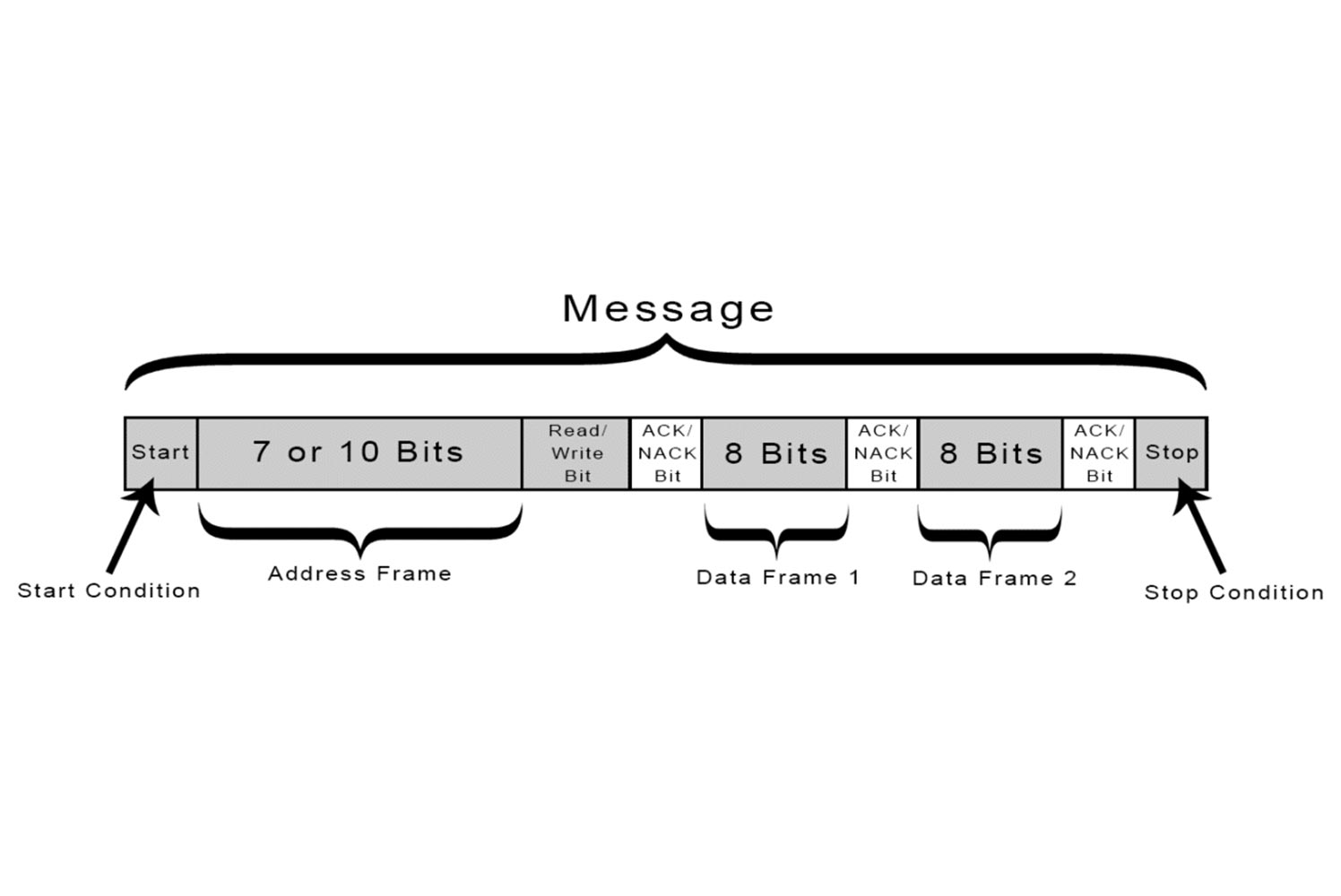
Start Condition : The SDA line switches from a high voltage level to a low voltage level before the SCL line switches from high to low.
Stop Condition : The SDA line switches from a low voltage level to a high voltage level after the SCL line switches from low to high.
Address Frame : 7 or 10 bit sequence unique to each slave that identifies the slave when the master wants to talk to it.
Read/Write Bit: A single bit specifying whether the master is sending data to the slave (low voltage level) or requesting data from it (high voltage level).
ACK/NACK Bit : Each frame in a message is followed by an acknowledge/no-acknowledge bit. If an address frame or data frame was successfully received, an ACK bit is returned to the sender from the receiving device.
ADDRESSING
I2C doesn’t have slave select lines like SPI, so it needs another way to let the slave know that data is being sent to it, and not another slave. It does this by addressing. The address frame is always the first frame after the start bit in a
new message.
The master sends the address of the slave it wants to communicate with every slave connected to it. Each slave then compares the address sent from the master to its address. If the address matches, it sends a low voltage ACK bit back to the
master. If the address doesn’t match, the slave does nothing and the SDA line remains high.
READ/WRITE BIT
The address frame includes a single bit at the end that informs the slave whether the master wants to write data to it or receive data from it. If the master wants to send data to the slave, the read/write bit is a low voltage level. If the master is requesting data from the slave, the bit is a high voltage level.
THE DATA FRAME
After the master detects the ACK bit from the slave, the first data frame is ready to be sent.
The data frame is always 8 bits long and sent with the most significant bit first. Each data frame is immediately followed by an ACK/NACK bit to verify that the frame has been received successfully. The ACK bit must be received by either the
master or the slave (depending on who is sending the data) before the next data frame can be sent.
After all of the data, frames have been sent, the master can send a stop condition to the slave to halt the transmission. The stop condition is a voltage transition from low to high on the SDA line after a low to high transition on the SCL
line, with the SCL line remaining high.
Click here to know the basics of I2C communication.
Process
Networking Boards
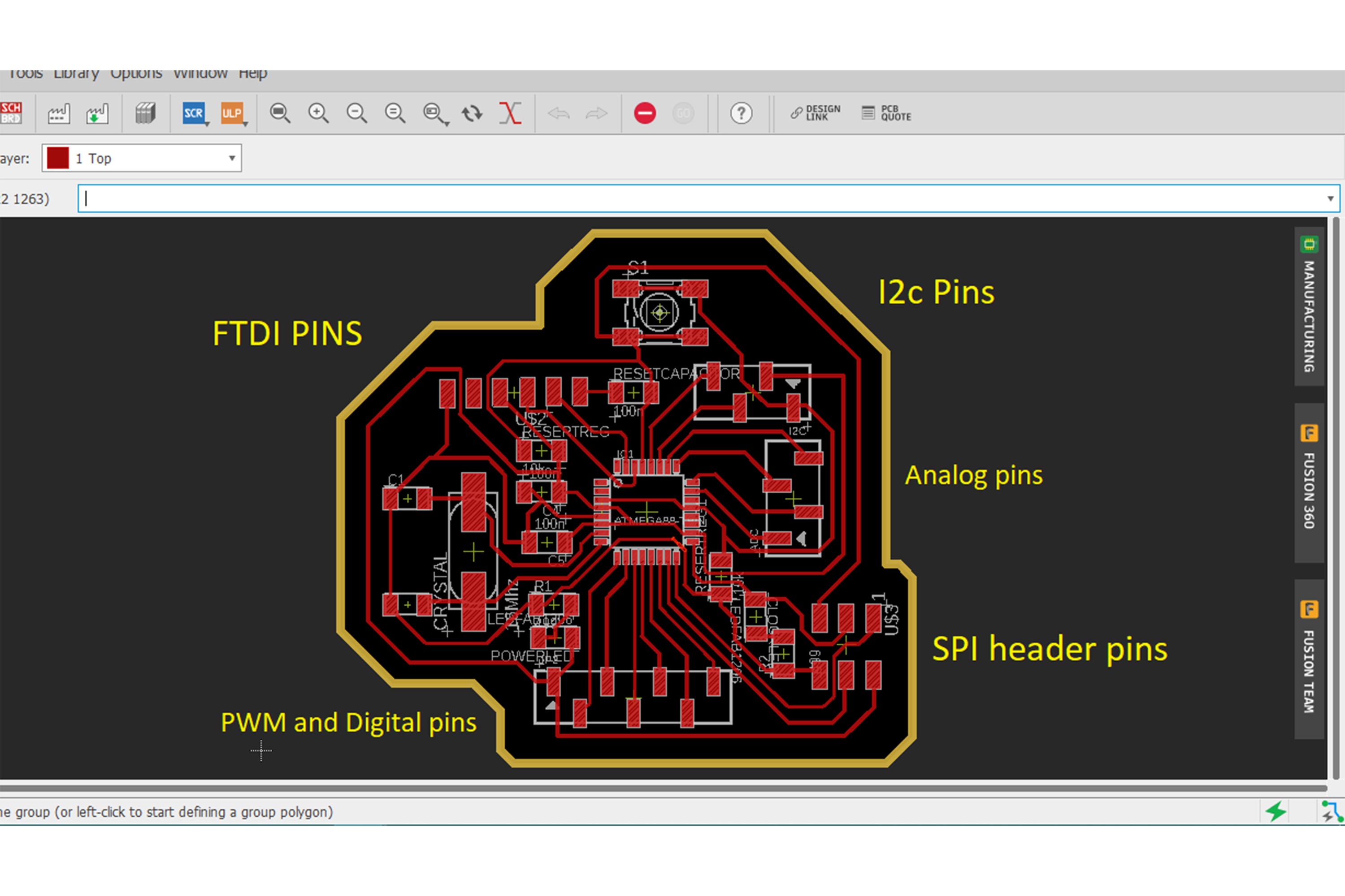
I designed new Networking boards for this week, this boards contain UART, SPI and I2C header pins. it has Some analog and Digital pins two, I gave two extra PWM pins additions to most and miso for running micro servos. one can see Eagle and PCB design In detail in week 7.
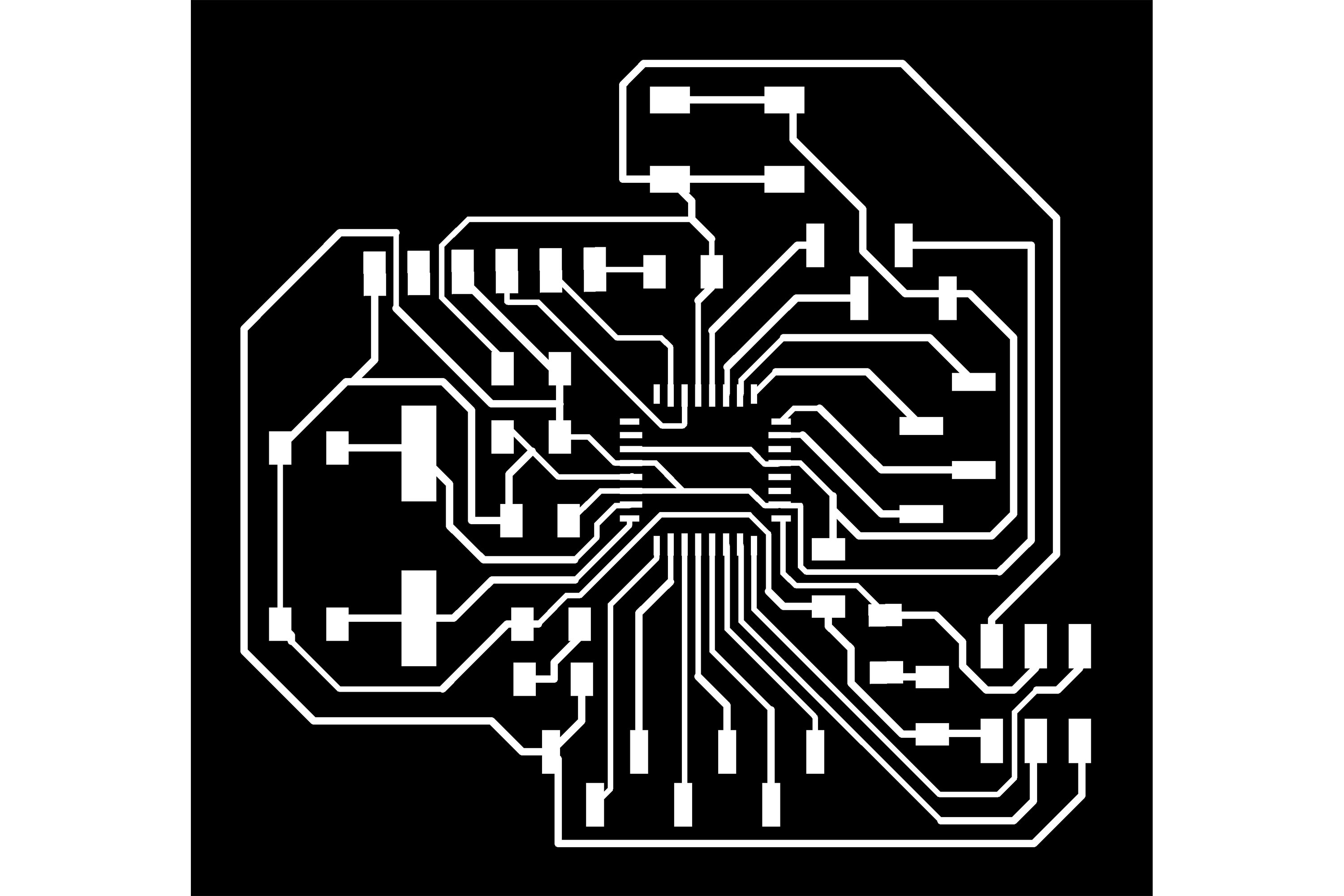
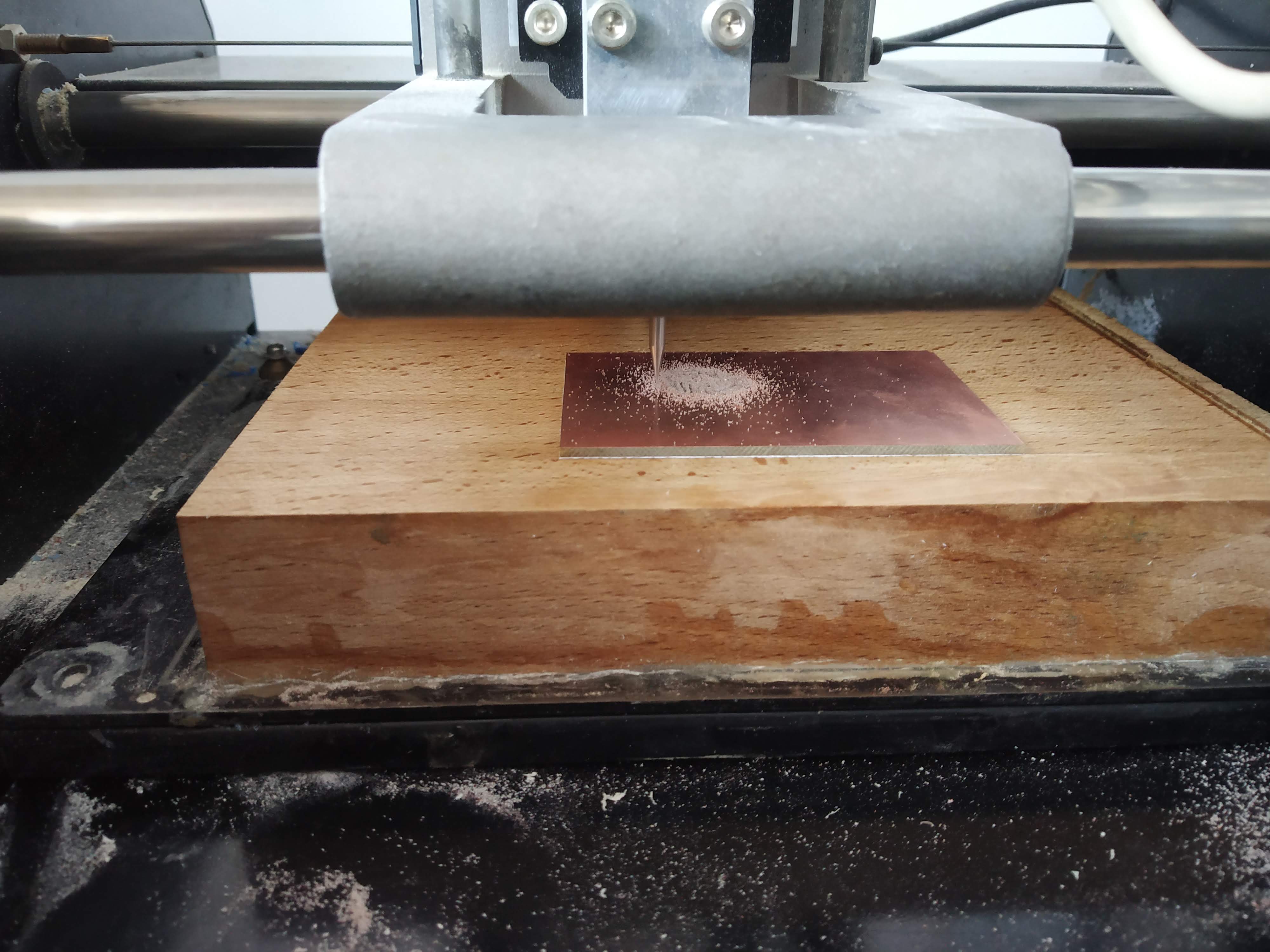
Exporting monochrome files
Then I exported Monochrome files of my board. below is Trace and Cut files of it. one can see these processes in Week 7

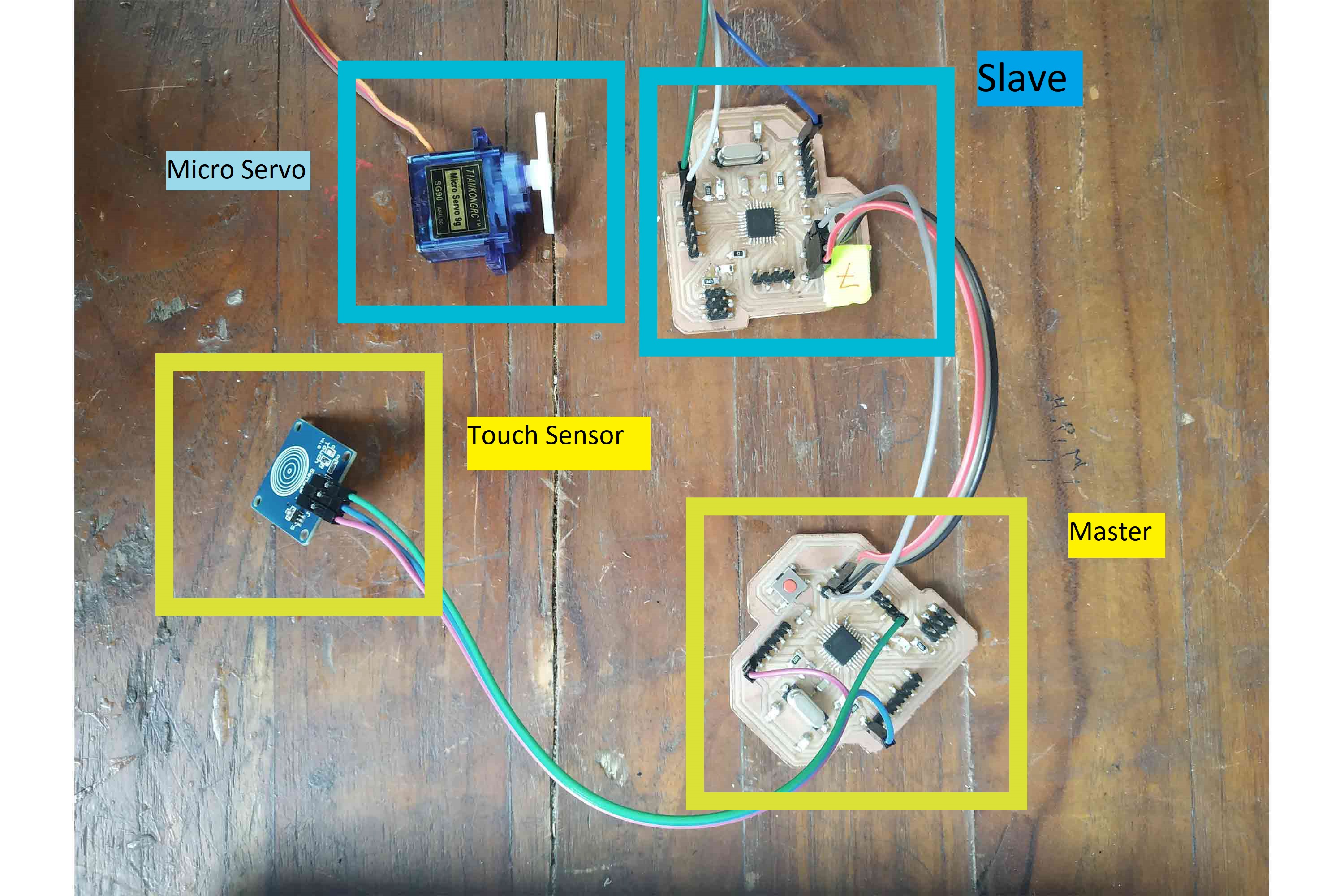
Input and output
Input : My input is Touch Sensor which is connected to Analog pin A0
Output : My output is Micro servo, I connected micro servo to PWM pin - 5
Code explanation
code explanation I have given in the comments if possible see it on Arduino IDE to avoid confusion.
//master code:

#include <Wire.h> // for i2c include wire library
int touch = A0;

void setup() { // setting up board rate and I/Os
  Serial.begin(9600);
  pinMode(touch,INPUT);
  pinMode(13,OUTPUT);
  Wire.begin(); // for i2c
}

void loop()
{
  int a = analogRead(touch); // reading values
  Serial.println(a); // for getting idea in serial monitor
  if ( a >=500) // if condition, if I touch the sensor, its analog value will be greagter then 500
  {
    digitalWrite(13,HIGH); // another signal of working of touch sensor
    Wire.beginTransmission(9); //slace number 8 // transmitting Address '9' though SDA  to slave
    Wire.write(1); // will give message of '1'
    Wire.endTransmission(); // end the transmition
    delay(200);
  }
  else
  {digitalWrite(13,LOW);
    Wire.beginTransmission(9);
    Wire.write(0); // if condition is not satisfy it will give '0' on message
    Wire.endTransmission();
    //delay(200);
  }


}
Slave
// slave code
#include  // wire library
#include  // servo library

int d1=0; // initialize d1
Servo myservo;

void setup() {
  pinMode(13,OUTPUT);
  myservo.attach(5);
  Serial.begin(9600);
  Wire.begin(9);     //address of the slave
  Wire.onReceive(recieveEvent); // will create recieve event
}

void loop() {

  if (d1 == 1) // if touch sensor is detecting something, master will write '1' and it will be sent to slave, see recieveevent below
    {
      digitalWrite(13, HIGH);
      myservo.write(180); // servo will go to 180
    } else if (d1 == 0)
    {
      digitalWrite(13, LOW);
      myservo.write(0); // if not it will go to 0
    } else
    {

    }


  delay(200);
}

// recieveevent : it will define d1's value
void recieveEvent(int howMany)
{
  while (Wire.available()) // if so0methoing is available
  {
    d1 = Wire.read(); // d1 will be equal to '1' or '0' depends on data written on slave by master
  }
}
Final video
Below you can see by touching the sensor servo will rotate at 180 degrees.
Group Work
In group work, we created an i2C and talk to multiple slaves through one master! In group work Master board is receiving the message through the serial and sending it to slaves to which we have given some address. in networking group work as
a contribution we all use our board to make one I2C bus.
Below is Video and for more information visit the group website.
Conclusion
This week was different with input and output week for me, one good thing was I don’t have to have one big board which have all the facilities for I/O sensors, one can use small modular boards which can do this tasks precisely, they will interrupt on each other less. Overall I gathered a good amount of information in I2C.