12. Output devices
This Weeks Task:
Group Assignment
- Measure the power consumption of an output device.
Individual Assignment
- Add an output device to a microcontroller board you’ve designed, and program it to do something.
Group Assignment
Here is the link to the group assignment page.
Individual Assignment
The output device that I will be using will be part of my final project which is the heating pad. I have also used two LED as indicators, red and green. Red light to indicate that it is heating and green light to indicate that the required temperature is reached.
In addition to the output devices, I have used an input device in this circuit since they will all be connected together. The input device used is the potentiometer and this circuit will be placed at the bottom of the model.
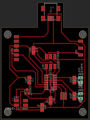
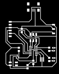
Schematic diagram
To create my schematic, I edited my echo hello board according to my requirements. Here is the schematic diagram.
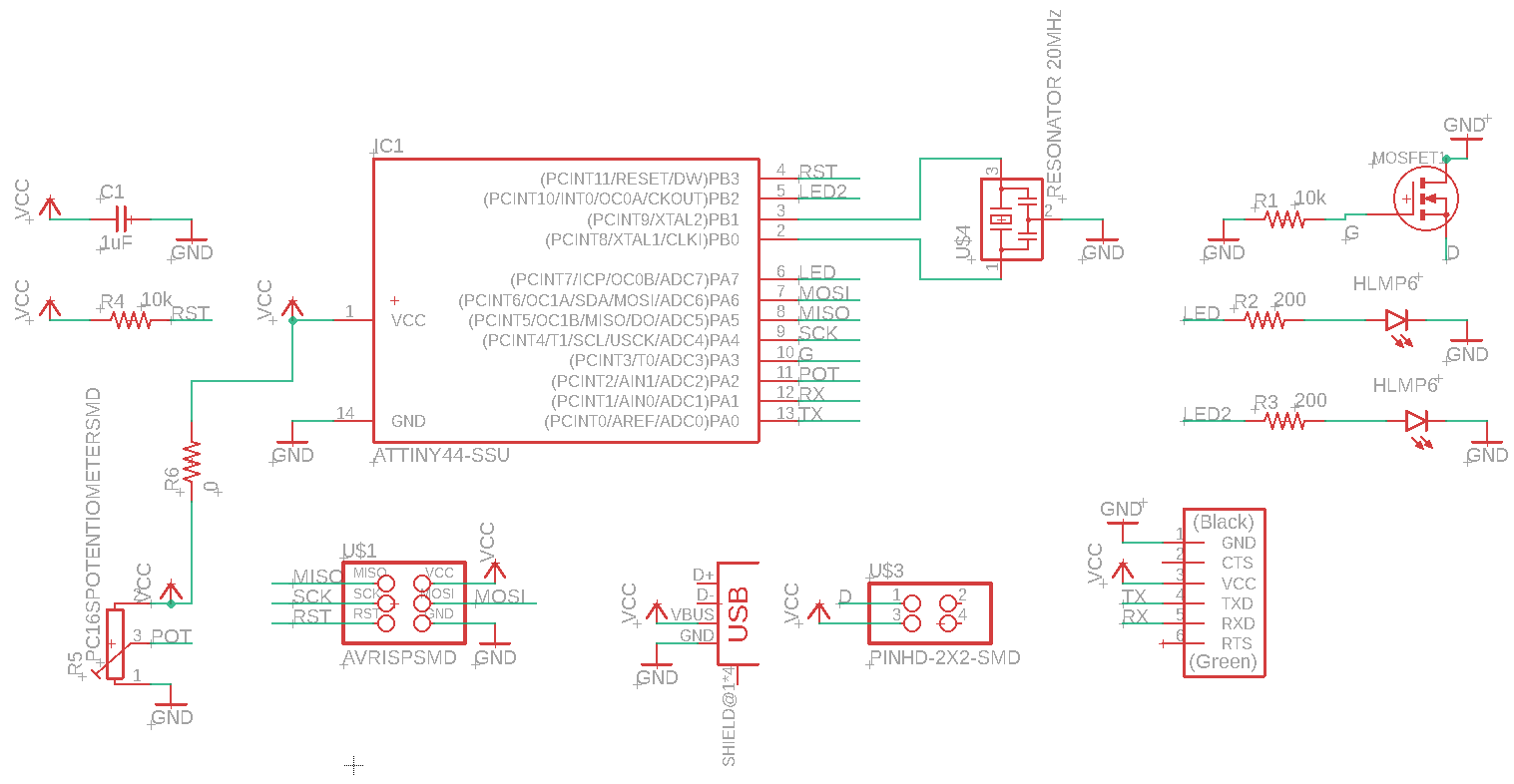
I have added a n channel mosfet for connecting the heating pad to the attiny 44. Here is the library that I used. One pin of the mosfet will be connected to a 2x2 header from which I will connect the heating pad here.
Moreover, I have added two through-hole LEDs since I want them to be visible to the user once the model is done.
For the potentiometer, since I have to connect it to a header and solder it, I had to design a new footprint for the header pins since the distance between each pin is less than the pitch distance of the potentiometer. Therefore, I have thought of soldering each header pin individually.
Steps for creating a new footprint
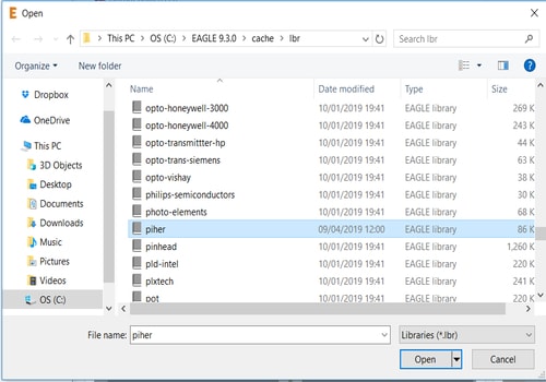
- In the schematic, I searched for the potentiometer in the existing eagle library to find its parent library.
-
Go to the control panel, File>Open>Library and select the library of the potentiometer.
-
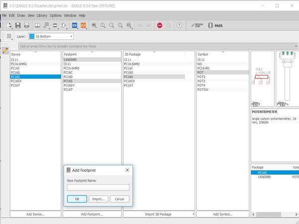
In the device column, click on the device name. In the footprint column, click on the Add footprint found at the bottom of the column. Click in Import in the Add footprint window.
-
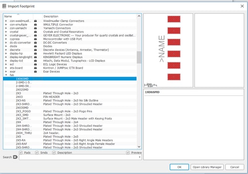
In my case, I just wanted to edit the FTDI header in the existing library according to what I need. Therefore, I selected this header.
-
After clicking on the header, it took me to a new page where I had to edit it.
-
I deleted the extra three pins (4,5,6) since I only needed 3 to connect the potentiometer. I also changed the distance between each pin by clicking on the info button in the left toolbar and then clicking on each pin. A window will appear in which I changed the position of the pins according to the pitch distance. Since I could not find any datasheets that had the pitch distance of the potentiometer, I had to measure it manually using a vernier and then typed in the position in the window. The pitch distance was found to be almost 4 mm in which I typed in as 150 mil ~ 3.81 mm.
-
Connecting pins
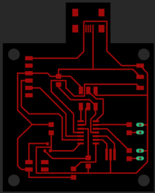
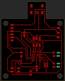
PCB design
Go to File>Switch to board to start with the pcb design. I adjusted the components and created the routing and below will be the final pcb design. I have also added four drill holes (3mm) to attach my circuit later with my model using screws.
Exporting the PCB
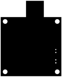
Go to ‘View’ > ‘Layer settings’ and select hide layers. This will remove all the layers on your board. You only want to show the top and pads layer since I have through-hole LEDs in my circuit. Therefore just click on the left side of the ‘Top and Pads Layer’ rows, so that the eye icon appears. Something like the image below will be displayed.
Then go to ‘File’ > ‘Export’ > ‘Image’ and change the resolutions settings to 500 DPI and select the monochrome. This file is the circuit traces image.
As per the circuit outline, I had to show the dimensions layer in addition to the top and pads layer. This will define the outline of my circuit. Export it and save it with the same settings as mentioned above.
Milling the board
After saving the the png images, I used Fab Modules to prepare them for milling.
Traces
- Insert image as png.
- Choose the output format as the machine you’re using for milling. In my case it was Roland mill (.rml)
- Choose the process as PCB traces (1/64).
- Adjust the output settings found at the right side of the image.
- Set the machine. In my case it was SRM-20
- Speed: 3mm/s
- x0: 0mm
- y0: 0mm
- z0: 0mm
- zjog: 12mm
- Click calculate and the image preview will show how the traces will get milled.
- Click save.
Outline
- Insert image as png.
- Choose the output format as the machine you’re using for milling. In my case it was Roland mill (.rml)
- Choose the process as PCB outline (1/32).
- Adjust the output settings found at the right side of the image.
- Set the machine. In my case it was SRM-20
- Speed: 0.5mm/s
- x0: 0mm
- y0: 0mm
- z0: 0mm
- zjog: 12mm
- Click calculate and the image preview will appear.
- Click save.
Open the VPanel to adjust the origin settings manually before milling. This defines the starting point of where the drill bit will be to start cutting. After adjusting the origins, allow the spindle to spin for 5 minutes atleast and then add the file you want mill and click on cut. Dont forget to change the drill bit while milling the traces and outline. The tool bit for traces is 1/64 and for outline is 1/32.
Soldering
Tools used:
- Sharp tweezers
- Solder flux pen
- Solder iron
- Solder
Components used:
- 20 MHz Resonator
- 0 ohm Resistor
- 2 10k ohm Resistor
- 2 200 ohm Resistor
- N channel Mosfet
- 1uF Capacitor
- IC1 ATTiny44
- FTDI header
- AVRISPSMD (2x3)
- AVRISPSMD (2x2)
- Heating Pad
- Red LED
- Green LED
- Potentiometer
- USB mini B
Here is an image of the pcb before soldering the components onto it.
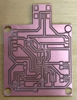
As shown, the drill holes were milled larger than the actual size given in eagle. The holes were supposed to be 3 mm, but in the pcb they measured at around 5 mm. In addition, the LED holes were not drilled completely. Therefore, I just inverted the colour in Fab modules and milled the circuit again.
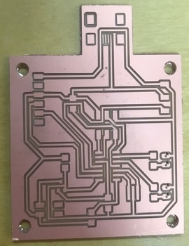
Here, the LED holes got misplaced in which we were not able to find the reason behind it. However, since the LED holes didnot interfere with anything else, I decided to continue with this circuit. The drill holes here clearly shows its smaller than the previous one and is 3 mm in diameter.
This is the final PCB.
Problems faced
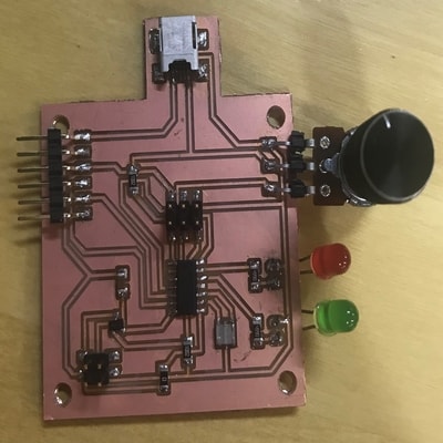
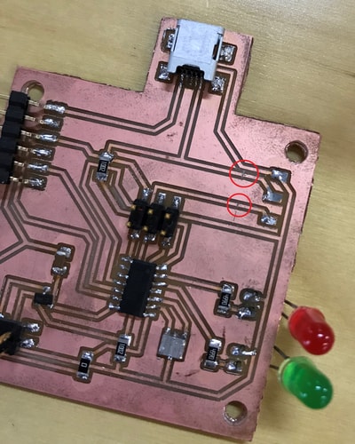
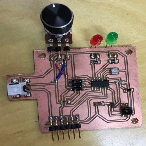
Unfortunately, the new footprint created for the potentiometer was wrong. The size of the footprint was fine but the connections to each pin was inaccurate. I accidently connected the middle pin to the vcc instead of connecting it to one of the attiny44 pins, and the third pin was accidently connected to the attiny44 pin. This was identified only after I completed soldering and checked the continuity test using the multimeter, from which it showed there was a connection between vcc and gnd. After observing the circuit connections, my instructor noticed the wrong potentiometer connections. As a result, I broke the track and connected them using a jumper instead of milling a new pcb again. This can be seen clearly in the images below.
Programming
Heating Pad
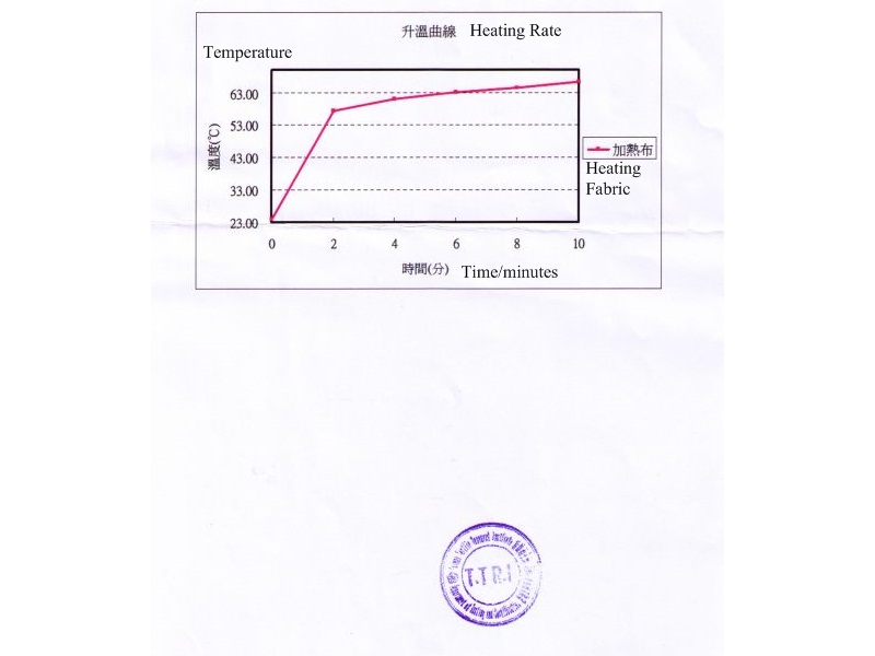
I edited the blink example in arduino so that it functions by only turning high so that it allows contiuous heating. This was just a test to check whether the heating pad works and heats up to the referrenced temperature (67 C) provided in the datasheet.
// the setup function runs once when you press reset or power the board

void setup() {
  pinMode(PA3, OUTPUT);
}

void loop() {
digitalWrite(PA3, HIGH);
}
This was a setup using the FTDI cable and my laptop usb port as the power source. The highest temperature it reached was 31 C.
This was a setup using the usb b mini cable and a power bank which was connected to a cable. I changed the power source in order to provide more current flow to check whether the temperature will increase or not. The highest temperature it reached was 36 C which is shown in the video.