1.INTRODUCTION
This week is similer to the electronics production week but I will design the board insteade of take a ready picture to mill, after the design we are going to mill our board and solder the components as the same as electronics production week.
To start this week we have to know some components and these components are:
1.Resistor
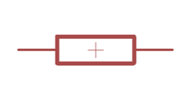
Resistor is part of an electrical circuit that resists the flow of current.
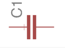
2.Capacetor
1.Resistor
2.Capacetor
Capacitor is a device used to store an electric charge, consisting of one or more pairs of conductors separated by an insulator. Capacitors are often used as filter devices to remove voltage or signal spikes in electronic circuits.
3.Led
4.Ground
Ground is the reference point relative to which other voltages in the circuit are measured. Vcc+ is positive relative to ground. We usually call the ground "zero volts", to make the other measurements simpler. Apply the black (-) end of your meter to ground on a powered circuit and the red (+) end of the meter on VCC to measure the voltage.
5.VCC
VCC (power) Vcc+ is positive relative to ground.
6.Pin Header
Header pins used to make the connection in female wires.
7.Integrated circuit
An integrated circuit (IC), sometimes called a chip or microchip, is a semiconductor wafer on which thousands or millions of tiny resistors, capacitors, and transistors are fabricated. An IC can function as an amplifier, oscillator, timer, counter, computer memory, or microprocessor. A particular IC is categorized as either linear (analog) or digital, depending on its intended application.
To know more about the IC we should read the
To know more about the IC we should read the
ATiny44 data sheet
And every component has a data sheet.2.EAGLE
What is Eagle?
EAGLE (Easily Applicable Graphical Layout Editor) is a flexible and expandable EDA schematic capture, PCB layout, autorouter and CAM program. EAGLE is popular among hobbyists because of its freeware license and rich availability of component libraries on the web.
In eagle there is some pharases we have to know:
1. schematics
A schematic in electronics is a drawing representing a circuit. It uses symbols to represent real-world electronic components. The most basic symbol is a simple conductor (traces), shown simply as a line. If wires connect in a diagram, they are shown with a dot at the intersection.
2.Board layout
The board layout shows how the electrical componets and traces will be laid out on the board. This is what the board layout looks like:
3.ADDING A NEW LIBRARY
This is the link of the library Fab.Ibr
To add the file to library copy the code and past it in text file then save it as fab.lbr after that past it on eagle library
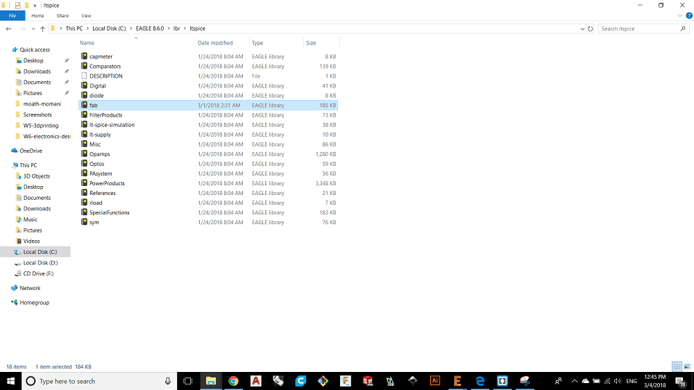
And then open Eagle and choose File - New - schematic
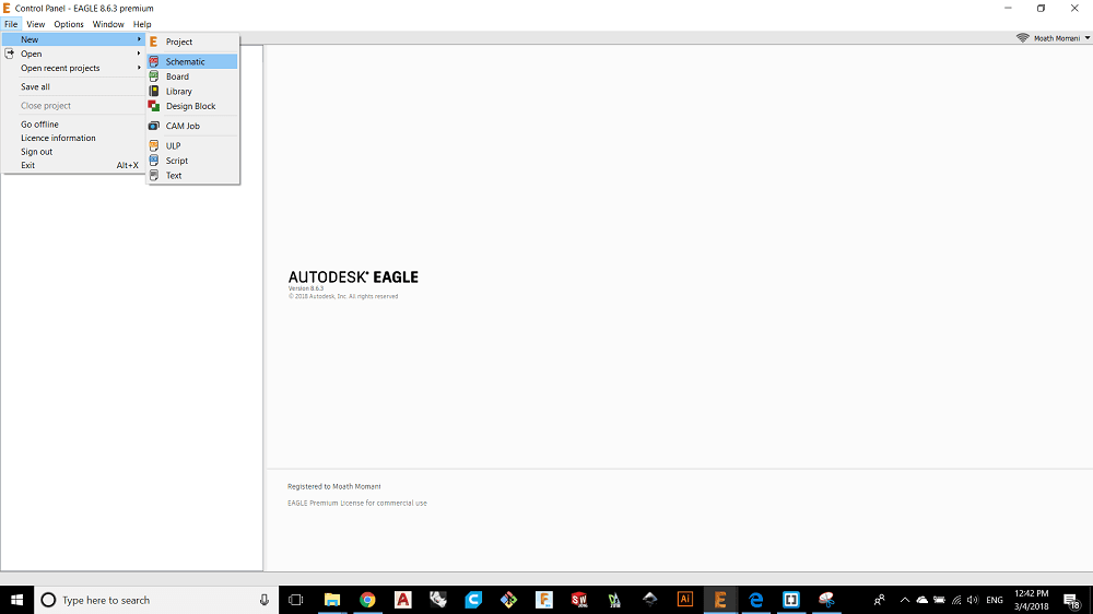
Now select Library-Open library manager
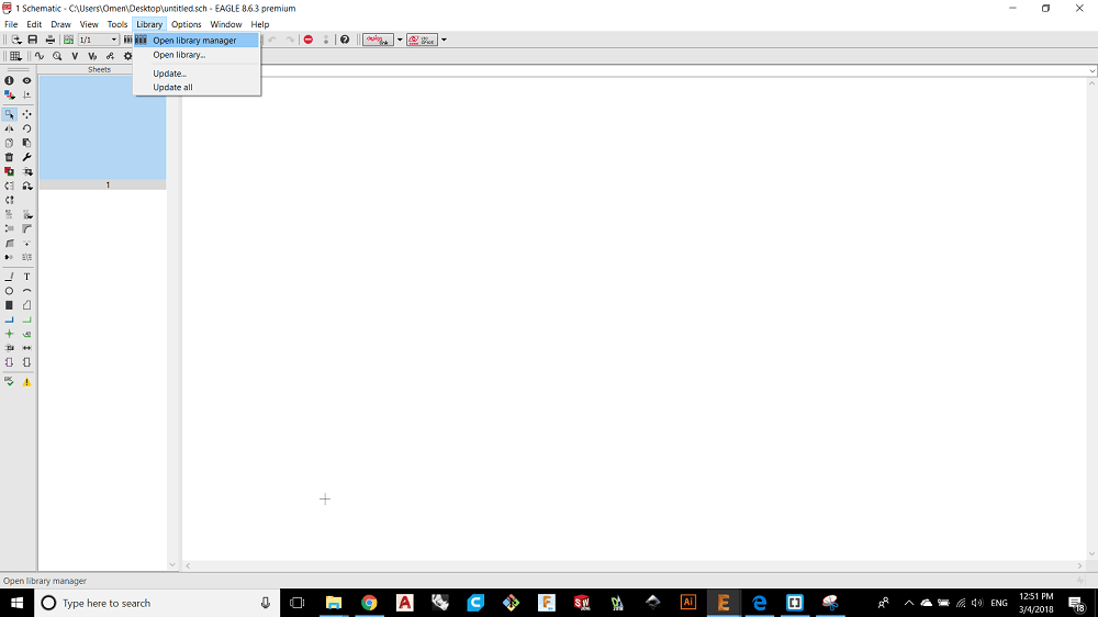
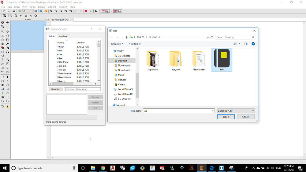
Select Browse and add the file
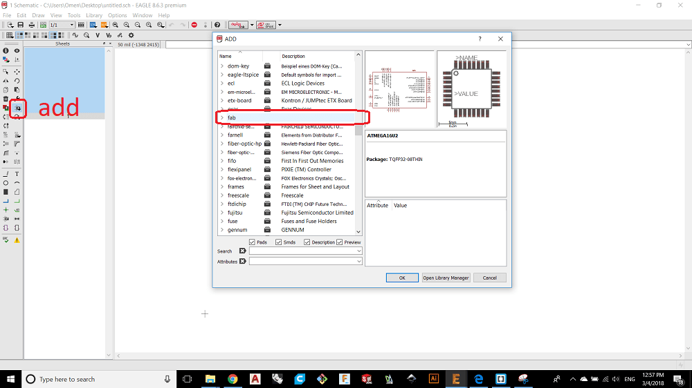
Final step, press add and you will find the FAB library :D
4.CAD Section
the first component is ATTINY44-SSU SOIC14 package which is an integrated circuit.
If we open the data sheet for ATTINY44 and look for pin configrations for SOIC package we well get this figure:
It is very important to read the data sheet to know the connections and configrations for the integrated circuit.
Now I added labels to connect the pins with other components, for example the pin number 1 is connected with the VCC in so thats mean all other components that have a vcc must be connected with pin 1, also labels used to avoid multiple connections.
After I opened the data sheet and understood the pin cofigrations I added the other components and they are: :
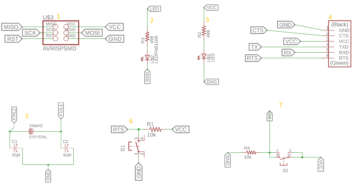
1.ATtiny44 microcontroller
2.Resistor 499 ohm
3.Resistor 499 ohm
4.FTDI-SMD-HEADER SMD 6pins.
5.20MHz CRYSTAL 2-SMD-5X3MM
6.Two capacitors10pf.
7.Two SMD SWITCH_6MM.
8.Two LED
Now its time to switch to board layout, we need a lot of time to spend in this part because we have to find a way to make many complecated connections as simple as possible and to avoid any overlapping, so you have to start changing the position and orientation of the components to find the easiest way to route them, the steps that we should follow in board layout are included step by step in this file tutorial
We can change the type of units for traces from grade icone and the trace width, the width that i used is 14 mil
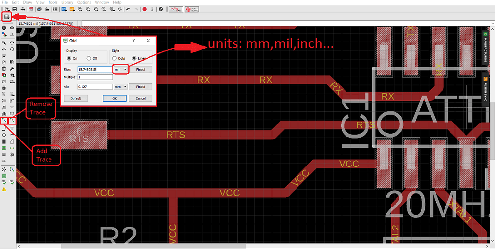
And this is how the good board looks like
Before saving my board as image to mill, I need to checked the errors by following these steps:
1. Download Fab Design Rules file
Or you can open this Link you will see this window so you can download it
Or copy the code and past it in a note file, after that SAVE THE FILE AS
dru
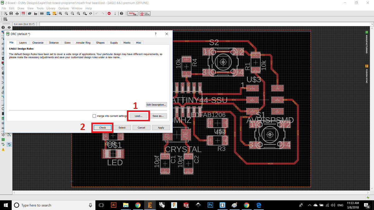
2. uploading the file to Eagle
From Tools choose DRC
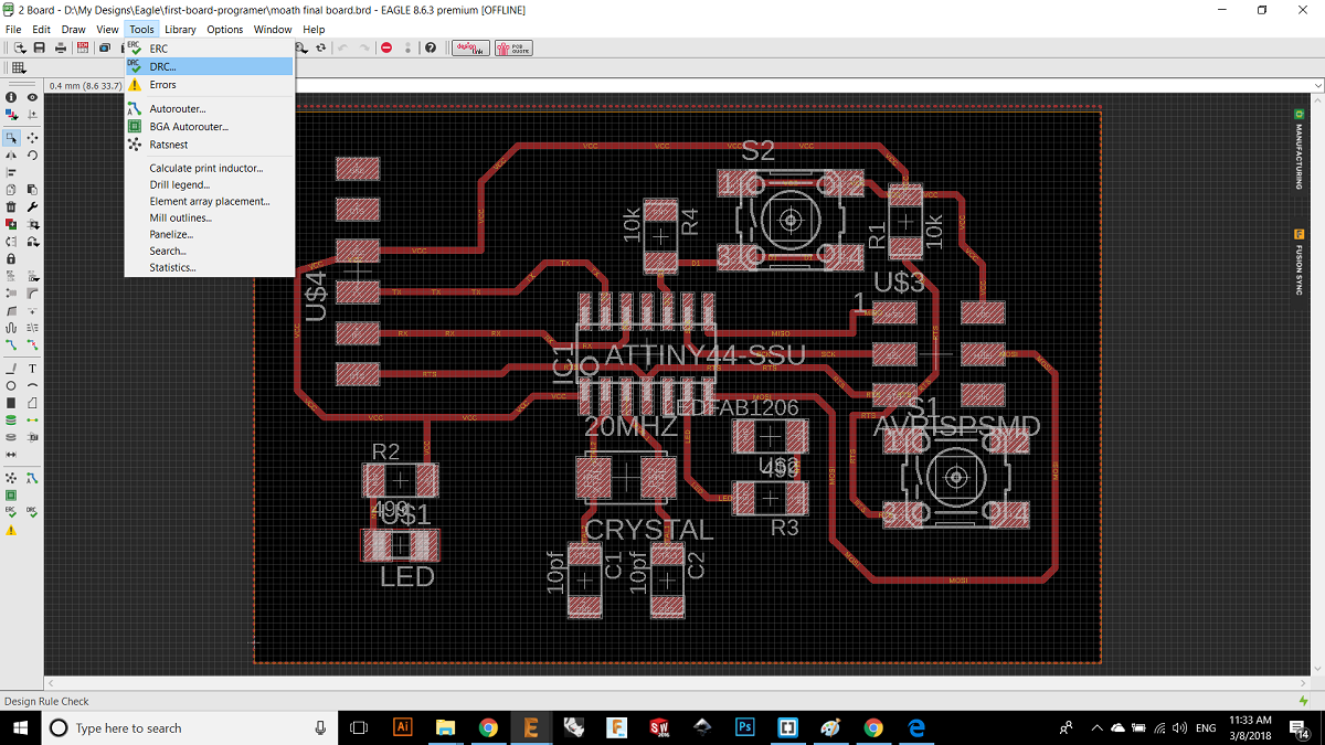
Load the file and click check as shown in the following
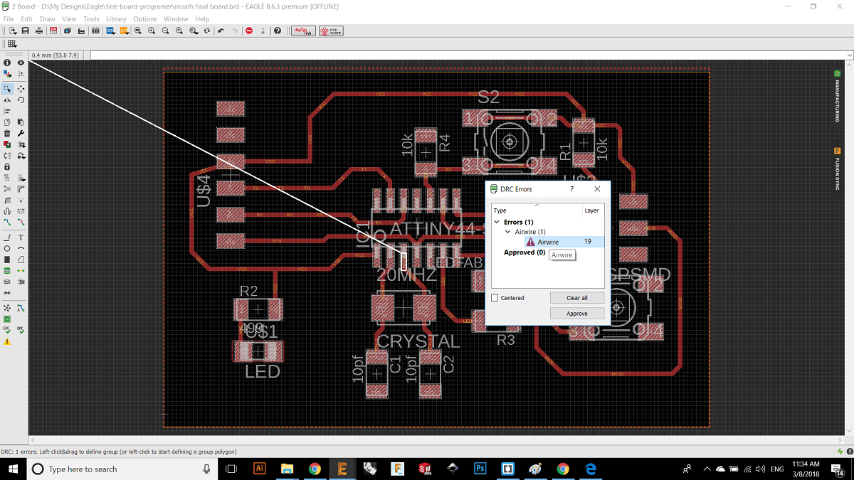
3. Correcting mistakes
Now we see the mistake of discontinuity in the trace and Atinny44, now make sure the tace is lined with IC and every thing will be okay.
Now its time to mill our board, so we need a picture to upload it on fab module, to save our board as image we follow those steps:
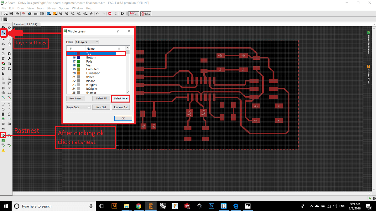
1.Open layer settings and select none then select Top
2.Export the file as image
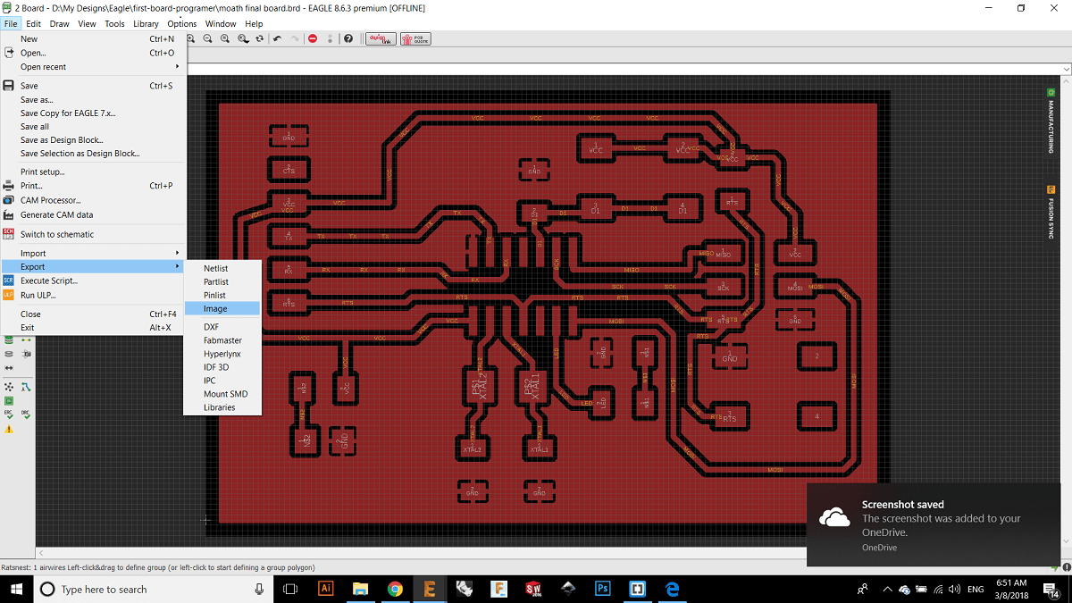
3.choose the resolution of 1500 and the other parameters
5.CAM SECTION
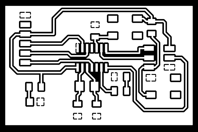
For inside cut
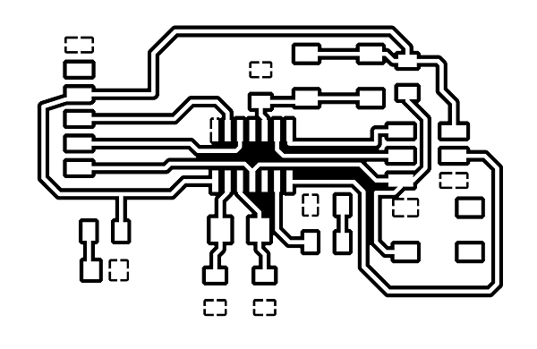
For outside cut

and this is my PCB :D
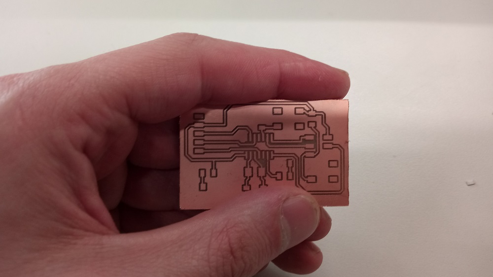
I collected all the needed components from the FabLab drawers:
1.AVR ISP SMD
2.Two Resistor 499 ohm plus two blue Leds
3.Pin HEADER SMD 6pins.
4.20MHz CRYSTAL 2-SMD-5X3MM and two capacitors.
5.Two Switchs 6mm.

6.PROGRAMING THE ECHO HELLO
After soldering the components I will program the board using arduino as an ISP.
The first thing I did was patch the arduino to recognize the Atmel Attiny44 microcontroller we used. To do that I followed the steps in this tutorial .
The first setup is to connect the arduino to my laptop and installed the arduino ISP from file-examples to my arduino, aftyer that I connected my board to the arduino using wires.
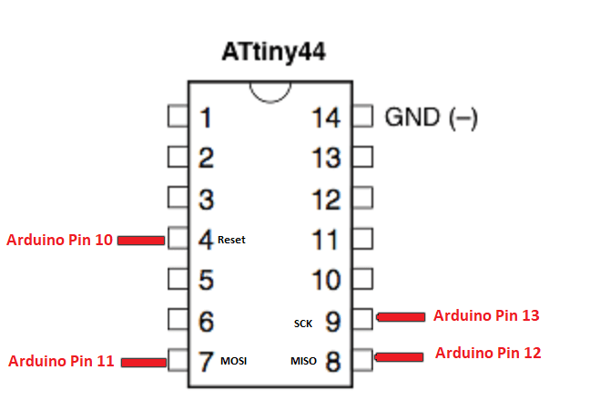
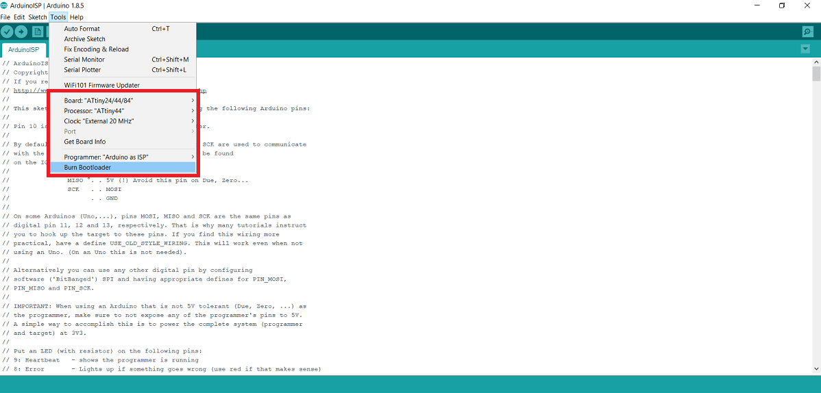
Then from TOOLS I checked that the board is Atinny 24/44/84 and the processor should be Atinny 44 and the clock 20MHZ and the programer is arduino as ISP then burn Bootloader.
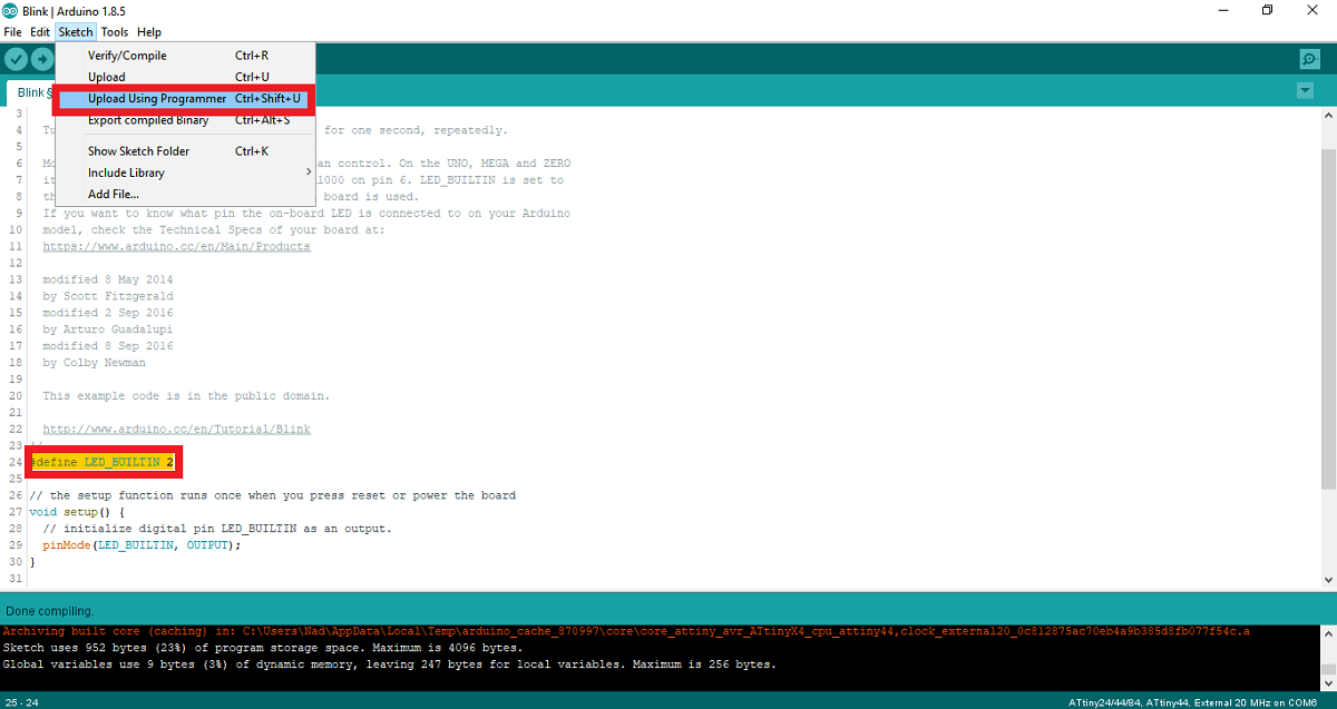
Next I wanted to make sure I could program it, so I chose to upload the blink example but after modyifying the pin to 2 after I read the data sheet, to upload it you should use upload using programmer instead of upload.
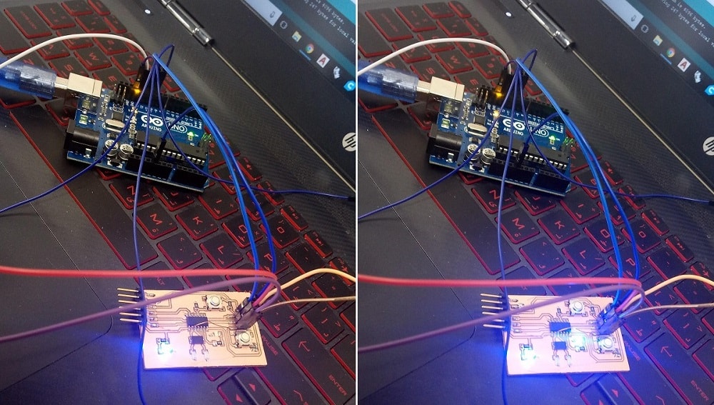
And here is my board plinking :D
Problems that I faced
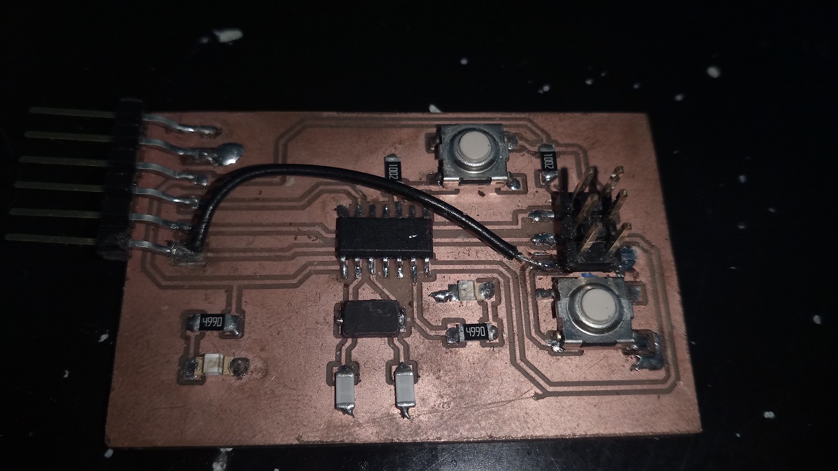
In the first design that I made for the first board hello echo board I forget to make the RST trace that connect the RST pin in pin header with the IC as shown in the next picture with the green color
So what I did to solve this problem is to connect the RST pins with each others by a wire
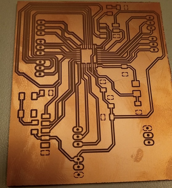
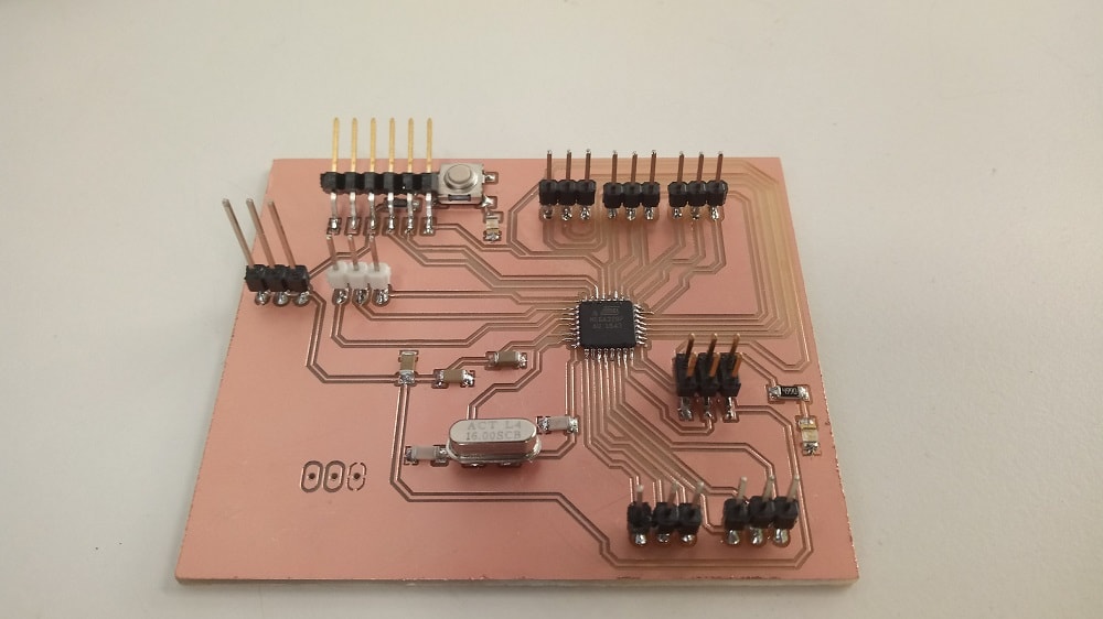
Second board with Atmega 328
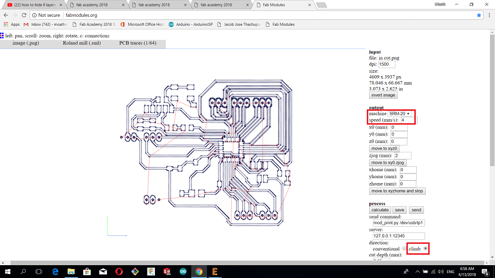
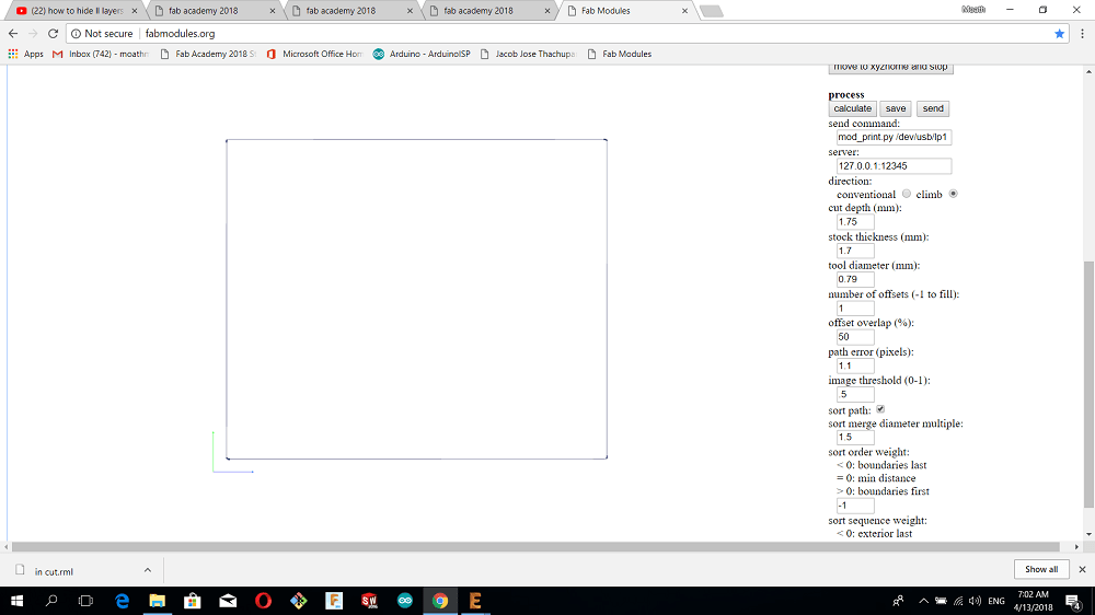
I used roland SRM-20 to mill my board, for the traces the bit was 1/64" ball nose and for outside or contour cut it was 1/32 flat and the board thickness was 1.7mm.
I saved the board design as image then I went to Fab modules to generate the toolpath.
#INSIDE CUT with depth of cut of .05mm
#OUTSIDE CUT with cutting feed rate of 0.5 mm/s
And here is my board
You can download my files here:
1.Hello board schematics
2.Hello board board
3.Inside cut image
4.Outside cut image
5. This is my second board schematic and board design
6.This is my second board outside cut and inside cut