WEEK 7 - ELECTRONICS DESIGN
INTRODUCTION
This week is a complementary work to week 5 where we learned the Electronics Production, Now it is time to know about the Electronics Design and know more about the design reasons and considerations when we create an Electronics Circuit as well as get familiar with the electronics components and its functionality.
Assignment Description
- Redraw the echo hello-world board.
- Add (at least) a button and LED (with current-limiting resistor).
- Check the design rules, make it (if you have time this week, test it).
- Measure its operation (Extra Credit) .
- Simulate its operation (Extra Credit) .
Learning Outcomes
- Select and use software for circuit board design.
- Demonstrate workflows used in circuit board design.
Have you (Checklist)
- ✔ Shown your process using words/images/screenshots
- ✔ Explained problems and how you fixed them, including how you worked with design rules for milling (DRC in EagleCad and KiCad).
- ✔ Included original design files (Eagle, KiCad, Inkscape, .cad - whatever)?
TOOLS AND HARDWARE USED (BOM):
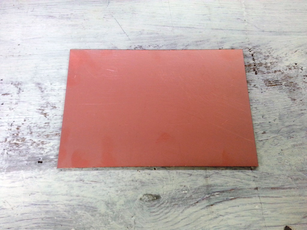
- 1 x FR1 (Copper PCB Board).
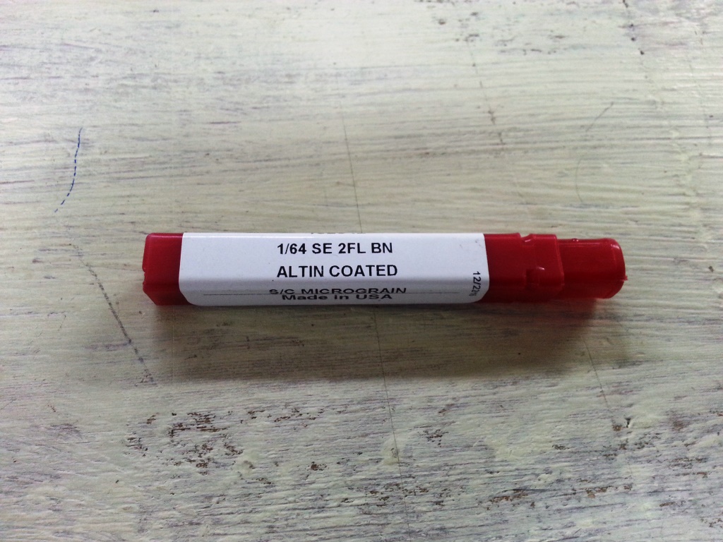
- 1 x 1/64 inch end mill bit.
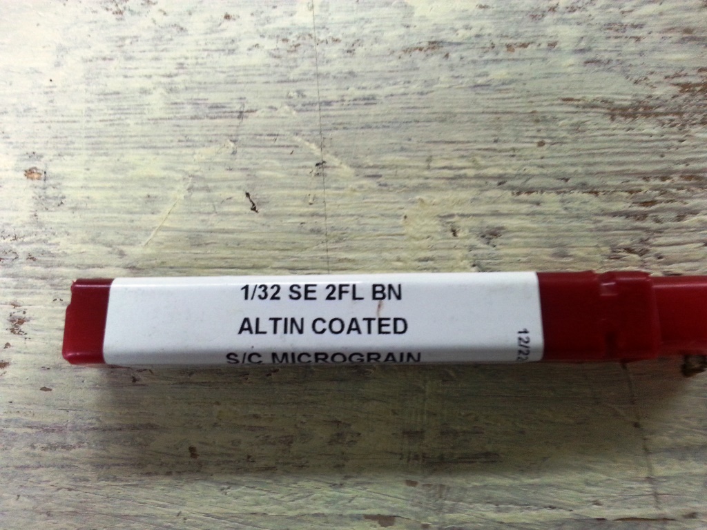
- 1 x 1/32 inch end mill bit.
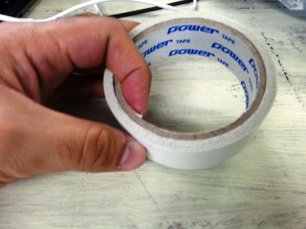
- 1 x double tape.
- 1 x Modela MDX-20 (More about the Machine can be found in THIS LINK
- 1 x Soldering Station.
- soldering wire
- AVO multimeter
- Electronic Components Including:
- 1 x Attiny 44 SSU.
- 1 x (2x3) pin header for AVRISP
- 1 x (1x6)pinheader for Rx,Tx,VCC,GND
- 1 x Red LED.
- 1 x Push Button.
- 1 x Resonator .
- 1 x 1 uF Capacitor.
- 1 x 10k Resistor
- 1 x 499 Resistor.
STEPS PERFORMED:
CIRCUIT DESIGN
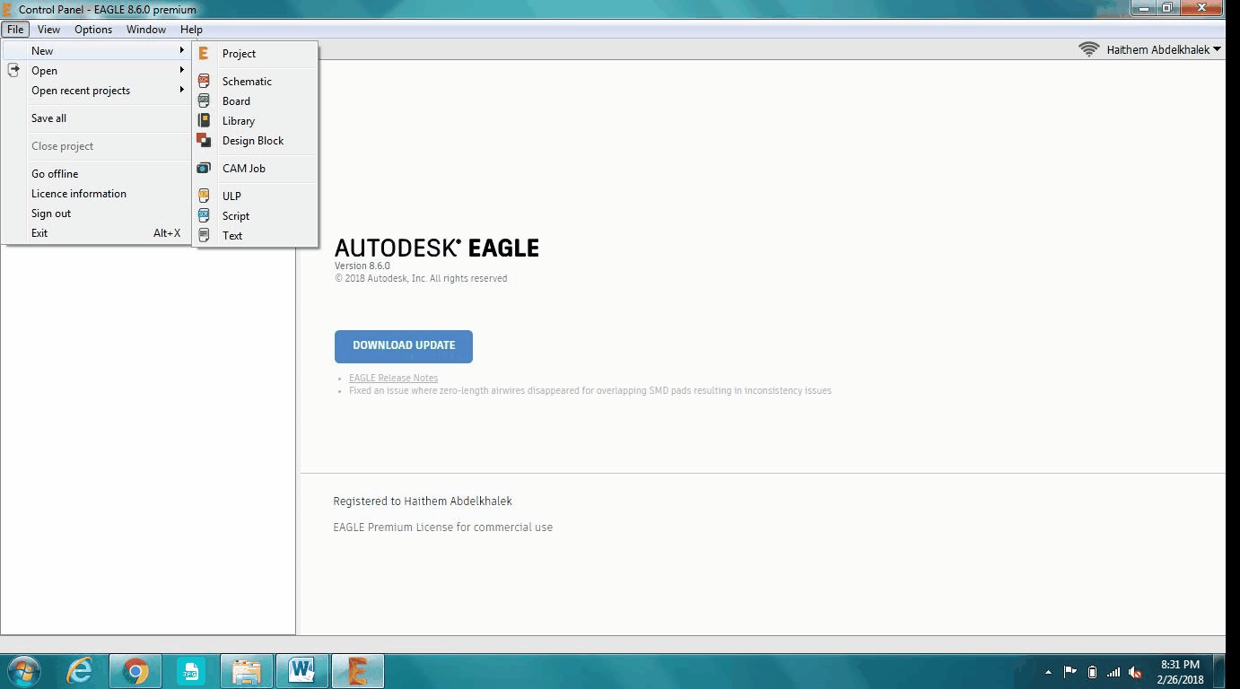
- I decided to use Autodesk Eagle as a CAD tool to design the circuit, I downloaded the new Autodesk Eagle unsing student license from THIS LINK and I installed it.
- If you do not have much experience dealing with Autodesk Eagle. I highly recommend that you go through THIS TUTORIAL before doing any of the coming steps.
- I started a new project and I then created a new schematic.
- I downloaded both the FAB lbr and Neil lbr files (Eagle Libraries with components to be used in this assignment).
- Go to the top toolbar and select the "Library" menu, select "use" and open the .lbr file(s) you downloaded.
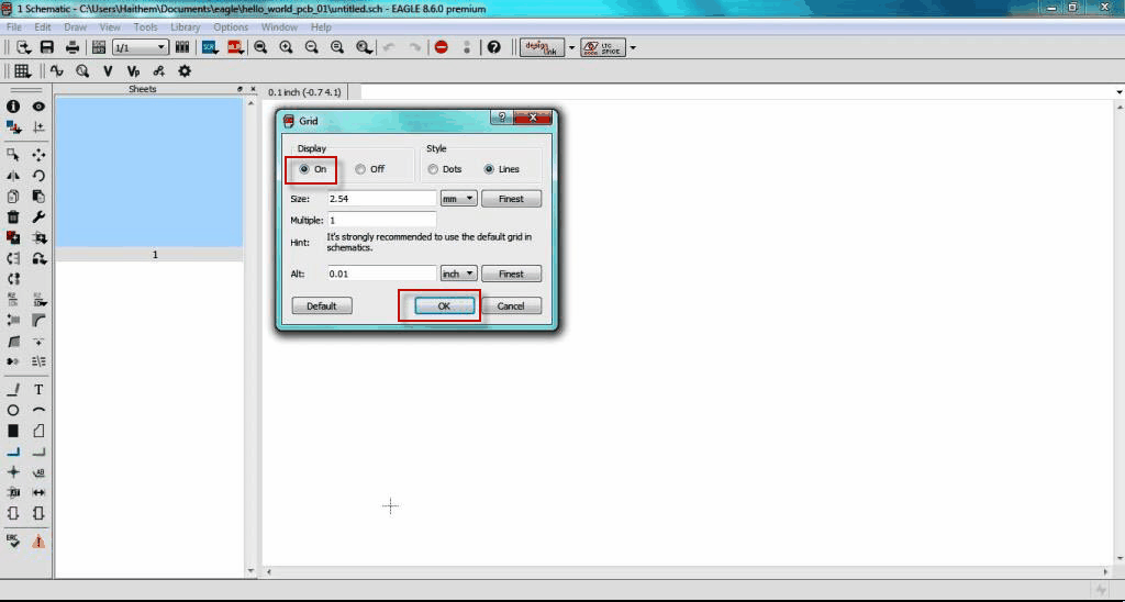
- I opened the schematic window and I configured the grid view to make it easier to align the components.
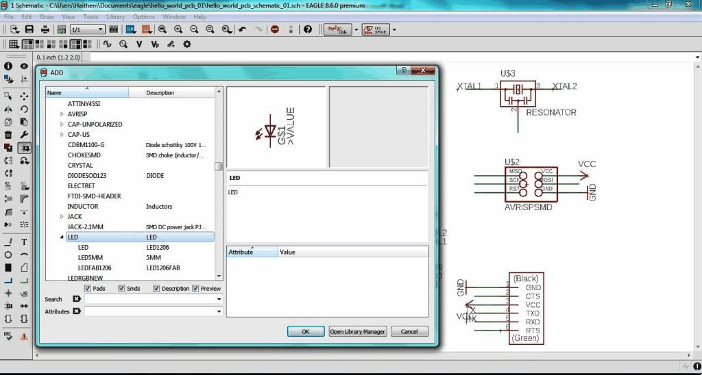
- To add a component: either type "add" or select the "add icon from the toolbar". The add menu will open. You can either look through the listed libraries (including the fab lbr) for a component to add or you can type it into the box above the "drop" button.
- Select the component you want, Click "ok" and then click on the schematic to place the component.
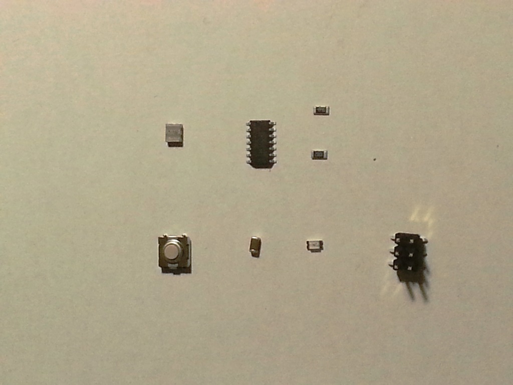
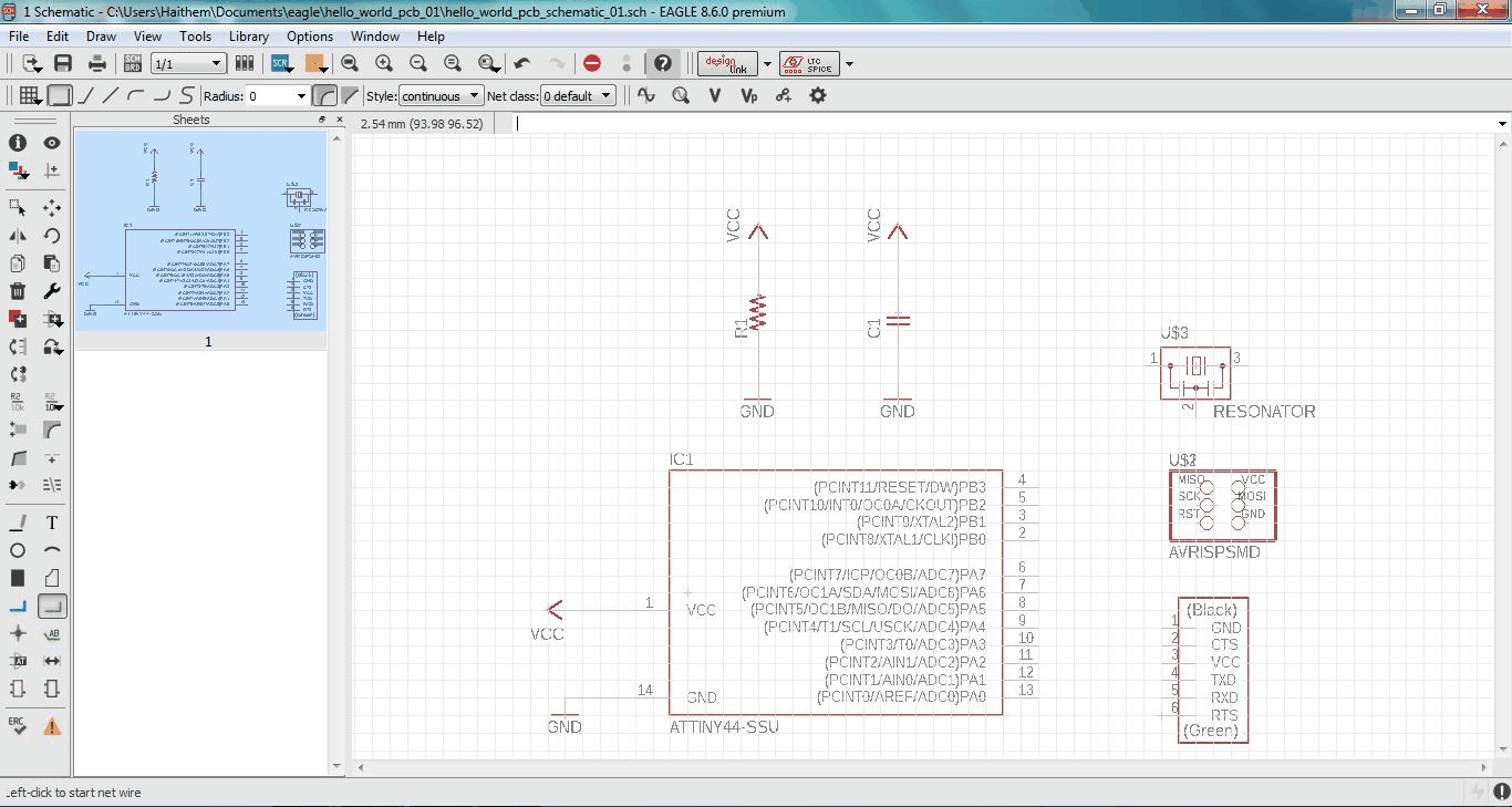
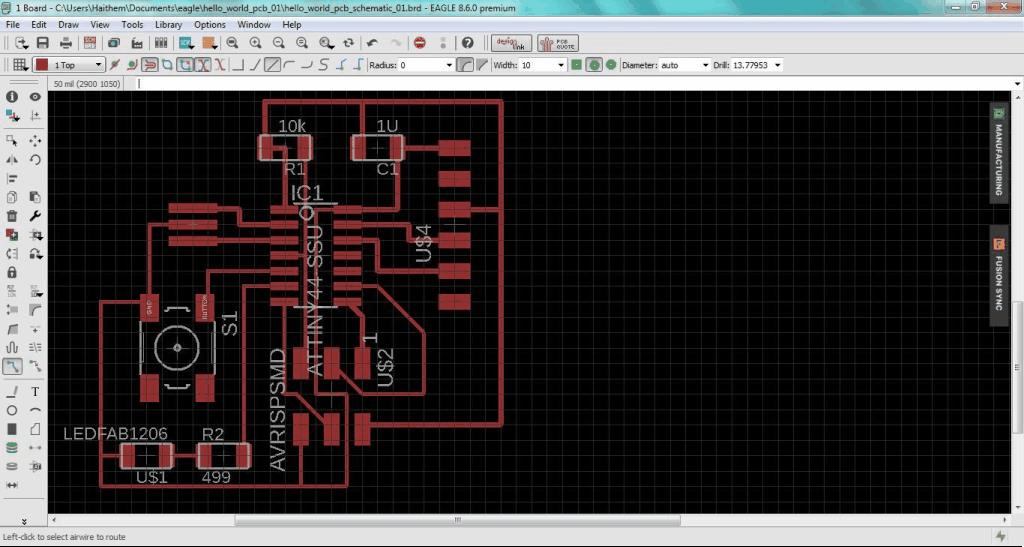
- I added the components as shown below:
- To connect the components, I used 2 ways: the wire tool (AKA "net" in Eagle) and nameing the nets attached to components that need to be connected by naming them with the same name. Eagle will ask if you want them to be connected, so accept that.
- Remember to name the component, then label it so the name appears in the diagram.
- I started to do this to all the connections needed in the circuit as shown below:
- I decided to add now the LED and the BUTTON from hte fab eagle library and connect them as shown below.
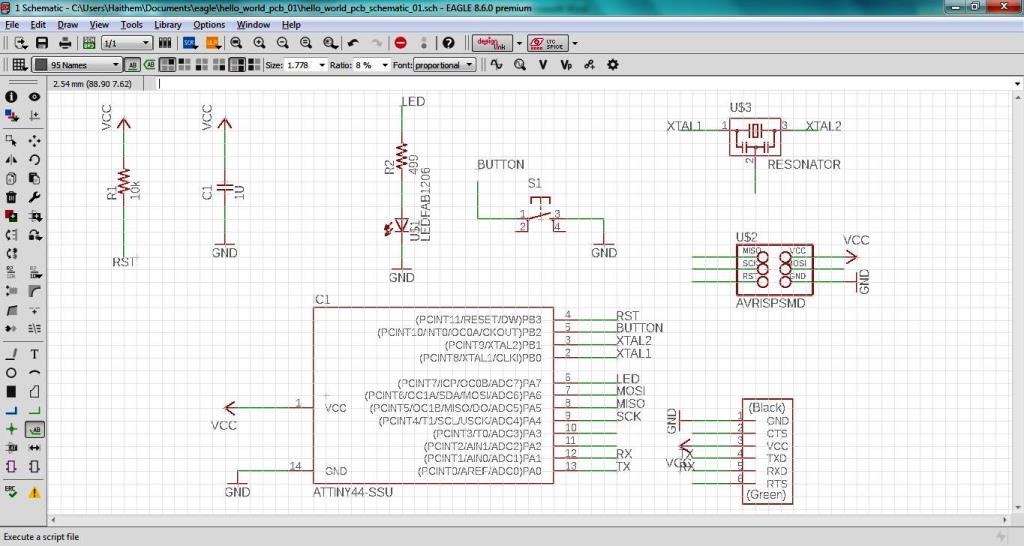
- Now Switch to the board view by going to the top menu > File > switch to board. The board view will open up and components you just added will appear
- Use "move" to move each component around and "route" to route each trace. The wire will turn red as you route it into place.
- Keep moving and adjusting the wires and components till you reach the final desired layout.
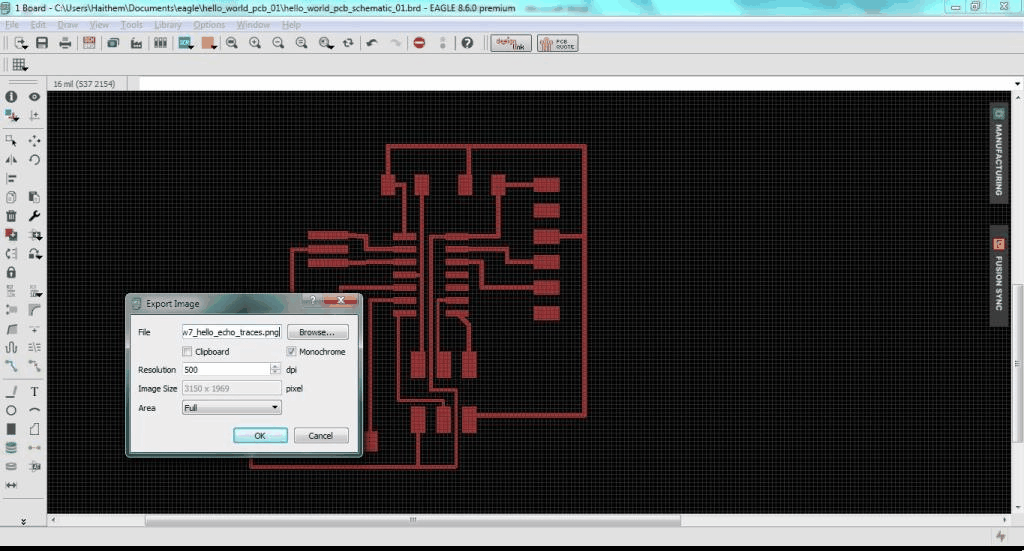
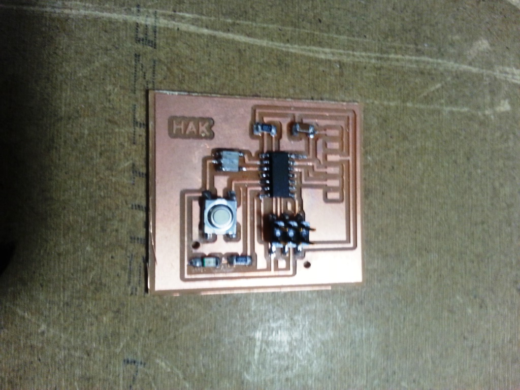
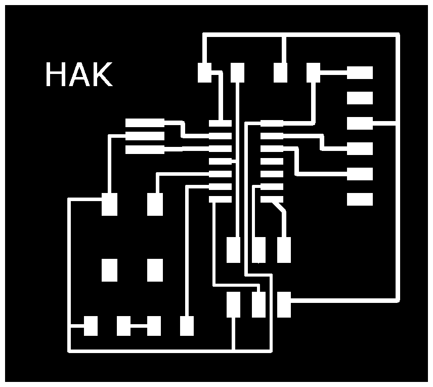
- After I finished the orientation and wiring the components in the board view I started to do the design check also known as DRC. the main purpose of te DRC is to ensure that the used 1/64 inch mill-bit tool will have enough clearance to mill around the traces and in-between them.
- a mill-bit with the diameter of 1/46 inch (~16 mil) is used; So I opened the DRC from The "Tools" menu. Then in the "Clearance" tab, I wrote "16mil" to all the fields there.

- Finally I started to export the circuit to PNG image as follows:
- In layers menu in the top toolbar, I selected the only the top layer (traces only)
- Export as a png (file -- export -- image)
- Choose settings: MONOCHROME and 500 DPI.
- Make sure the color mode is set to greyscale: image > mode > greyscale
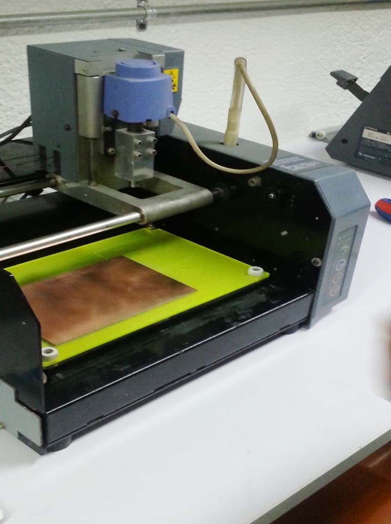
MILLING THE CIRCUIT
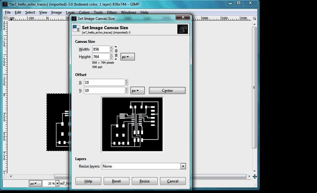
- Now before the milling I decided to work on the exported PNG files using GIMP to tweak the Traces and Interior PNG files.
- I opened GIMP, I opened the file I exported from Eagle and then I used the "Rectangle Select" tool, I selected the inner border of the dimension rectangle and then right-click->Image->Crop To Selection.
- To add a border, I clicked Image->Canvas Size and added 20px to width and height and the clicked on the "Center" button.
- Then to make the border white, I clicked Image->Flatten Image. Then saved the image.
- Finally using the "Bucket Fill Tool", I blackened all the traces so that I'm left with only a white border and I inverted the color to get white borders.
- I exported the created files as PNG, Now we are ready for milling.
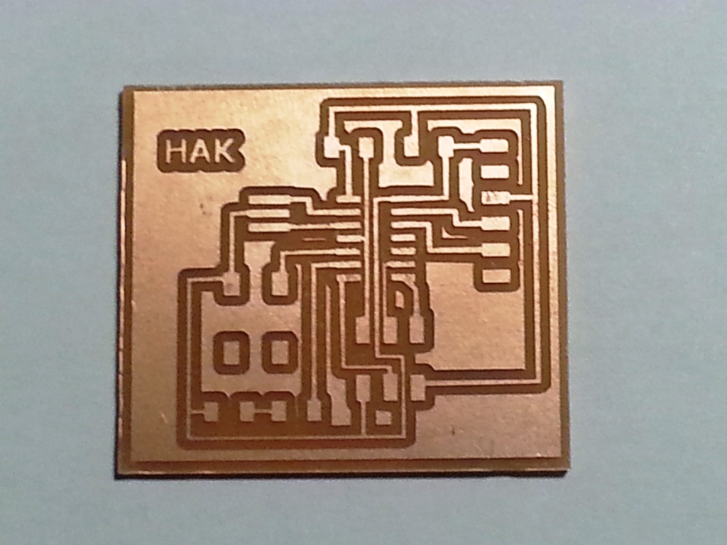
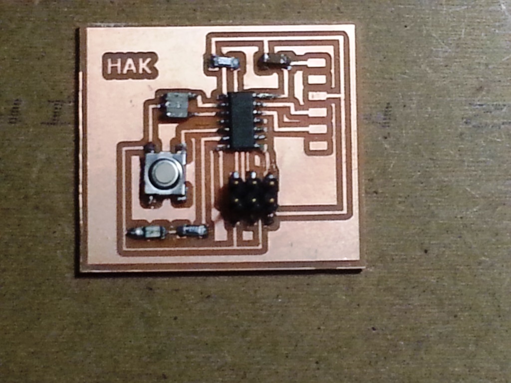
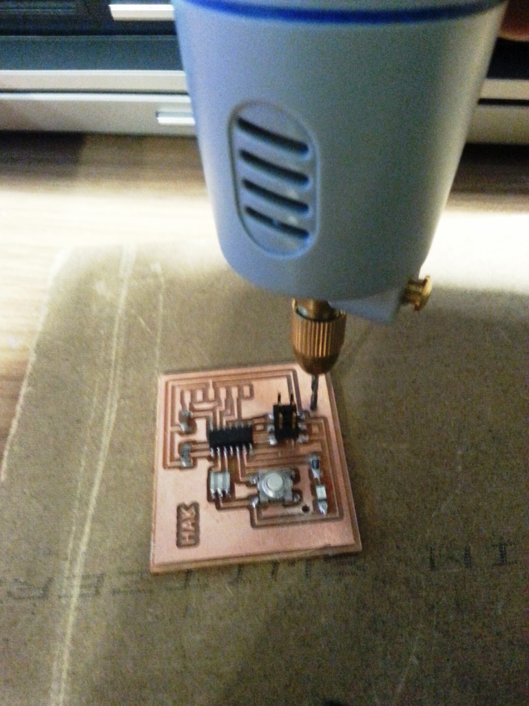
- I started milling the circuit PCB baard on the Modela MDX-20 using Fabmodules and soldering the components follwoing the same principles we learned in WEEK 5 assignment as shown in the video below:
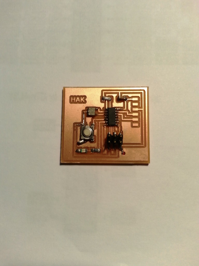
- I soldered the electronic components in the PCB circuit as shown below and I did the following activities during soldering: .
- I did check for the connectivity and the quality of soldering after soldering each component using the "Connectivity Test" in the AVO meter.
- I did check for short circuit using the "Connectivity Test" in the AVO meter.
TESTING CIRCUIT OPERATION (PROGRAMMING)
PROGRAMMING USING ARDUINO IDE AND ARDUINO AS A PROGRAMMER
- I decided to burn the bootloader on the ATTINY44 Controller and upload the BLINK Arduino sketch on it using an arduino uno board that I have.
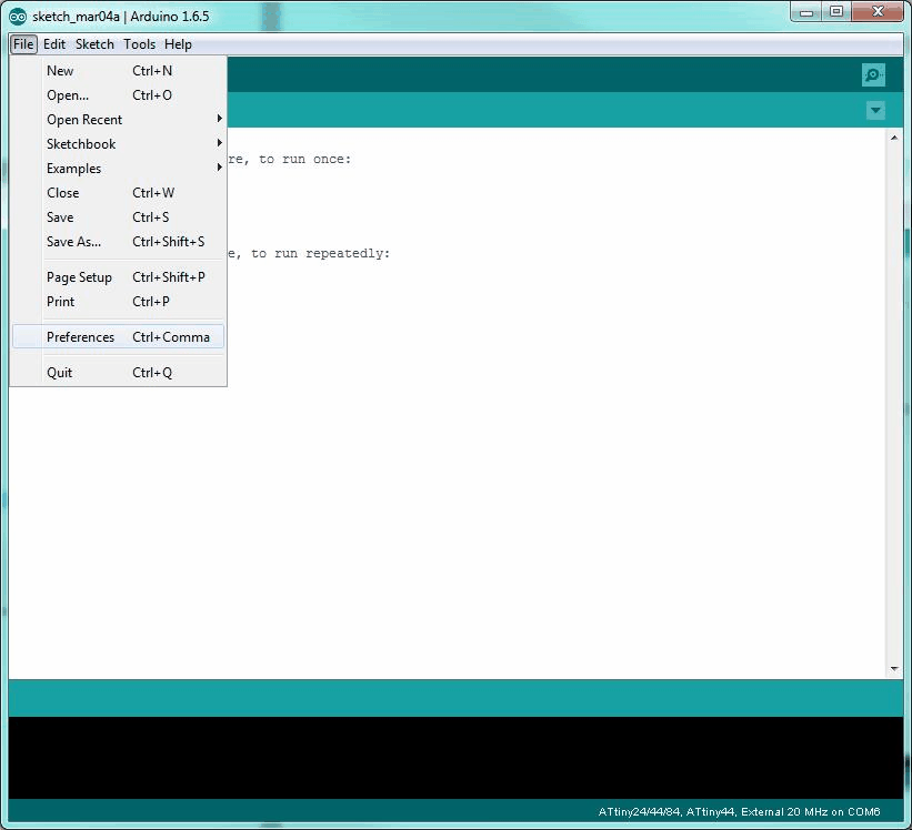
- I added support to the ATTINY44 to my arduino IDE:
- Open File > Preferences, Then, at the bottom of the pop up menu where you see "Additional Boards Manager URLs" copy and paste "https://raw.githubusercontent.com/damellis/attiny/ide-1.6.x-boards-manager/package_damellis_attiny_index.json" and click OK
- Go to Tools > Board > Board Manager, scroll down to the bottom and you should find "attiny". Click the install button and the words "Installed" should appear when the task is complete.
- To confirm that you have added support for the boards, navigate to Tools > Board and you should see ATtiny at the bottom of the list.
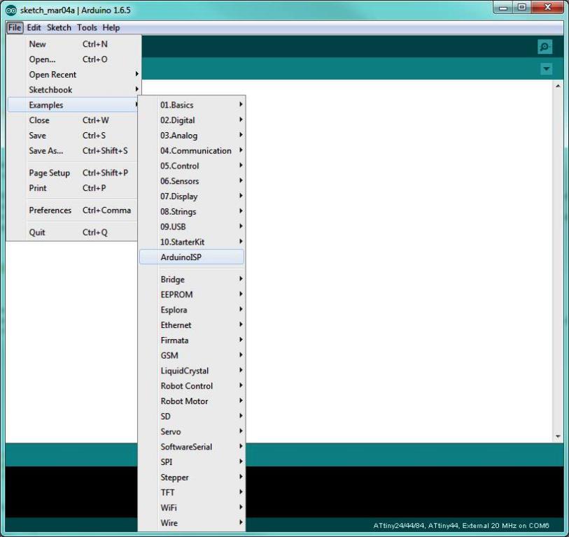
- Go to File > Examples > ArduinoISP. Open the sketch and upload it to your Arduino.
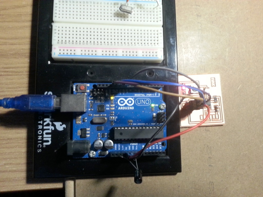
- Connect 10 μF Capacitor to the Ground and Reset Pins on the Arduino. Make sure the ground side of the capacitor (Typically the side with a silver stripe) goes into the Ground pin on the board. This will help act as a filter and stop the Arduino from resetting itself when programming the ATtiny.
- Connect jumper wires as follows:
- Arduino Pin 13 ---> SCK
- Arduino Pin 12 ---> MISO
- Arduino Pin 11 ---> MOSI
- Arduino Pin 10 ---> RESET
- Arduino 5V ---> VCC
- Arduino Ground ---> GND
- To burn the BOOTLOADER I followed the following steps:
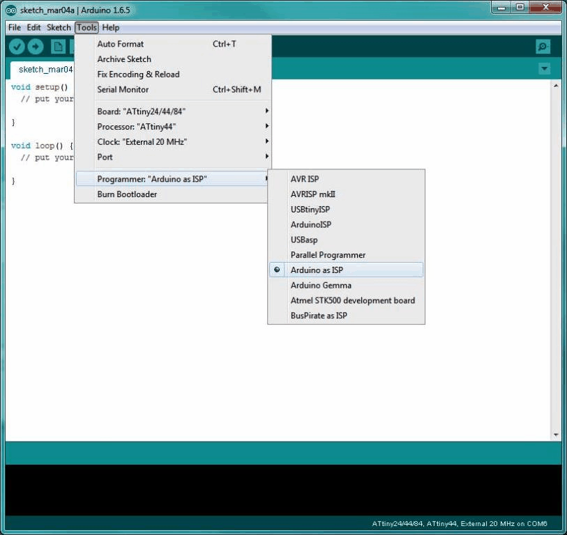
- Select "Arduino as ISP" under Tools > Programmer.
- Select ATtiny from Tools > Board.
- Select the specific ATtiny you are using (44/45/84/85) from Tools > Processor.
- Next select "20 MHz (External)" from Tools > Clock.
- select "Burn Bootloader" under tools and wait till it complete.
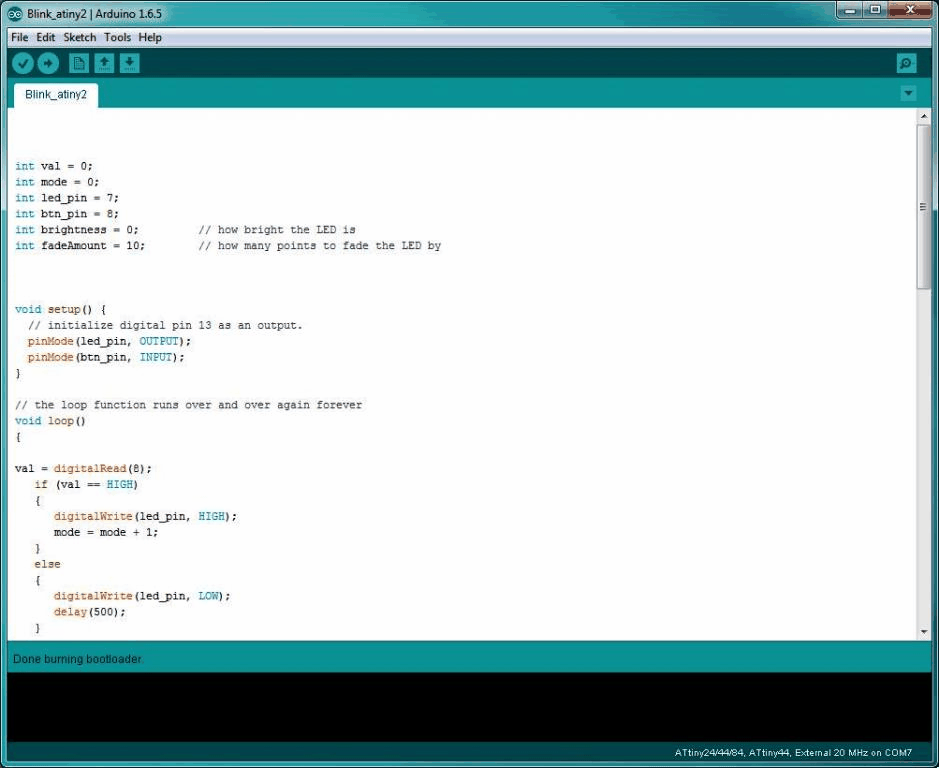
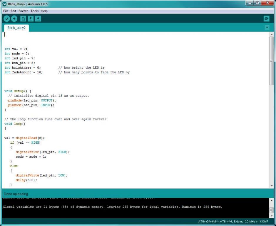
- To upload the BLINK code:
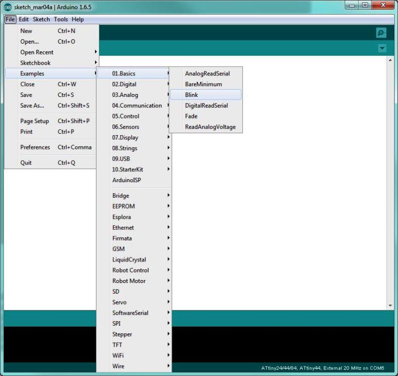
- Open File > Examples > Basic > Blink.
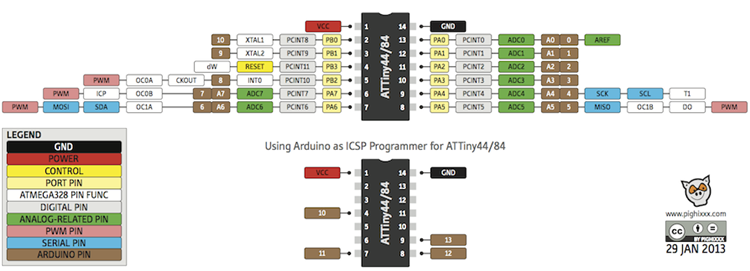
- From the diagram below, locate the PIN where the LED is connected to the ATTINY44 chip to and identify its mapped Arduino PIN number (in my case it was 7)
- Modify the PIN number to be 7 in the Sketch.
- Make sure you have the correct Board (i.e: ATTINY44, 20 Mhz Clock, and Processor selected under the Tools Menu, then click upload
- Result is SUCCESS!, the LED should be blinking which means the PCB work fine.
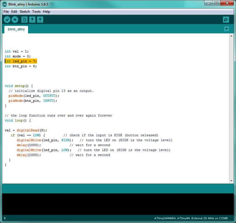
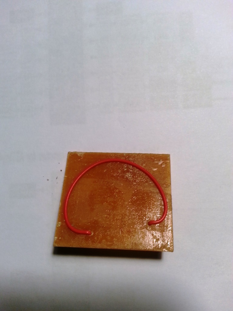
REWORK! - When I tried to make the button as an input to force the led to operate in several modes, I discovered that this is almost impossible as I connected the button to the ground, hence whether the button is pressed or not the status of the ATTINY pin will always be LOW. So I decided to do the following rework!.
Later I discovered that this could also have been achieved by software by enabling the pull-up resistor simply by “pinMode(btn_pi, INPUT_PULLUP)”
- I drilled 2 small holes in the board and connected them using a jumper wire, then I soldered the 2 ends of the wire with one end soldered to the VCC Pin and the other end to the button.
- I also disconnected the button Pin that was connected to the GND. This way whenever we press the button the ATTINY PIN connected to the button will get HIGH signal.
- I then modified the Arduino Sketch so that whenever the button is pressed it toggle between different modes, one mode make it blink, one mode make it fade in and out and so on.
PROGRAMMING USING ARDUINO IDE AND FABISP AS A PROGRAMMER
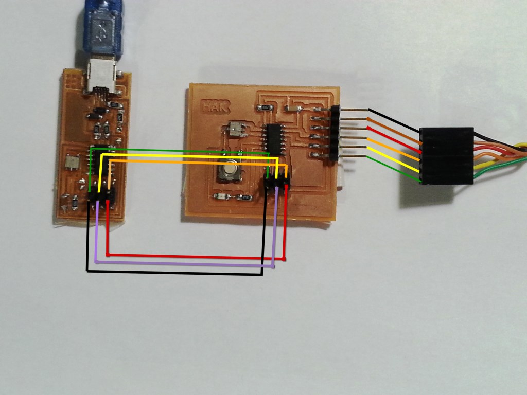
- Connect the FAB ISP pins to the Hello board pins with each pin connected to its corresponding similar pin as follows:
- MISO (in FAB ISP) -> MISO (in Hello Board)
- MOSI (in FAB ISP) -> MOSI (in Hello Board)
- SCK (in FAB ISP) -> SCK (in Hello Board)
- Vcc (in FAB ISP) -> Vcc (in Hello Board)
- GND (in FAB ISP) -> GND (in Hello Board)
- RST (in FAB ISP) -> RST (in Hello Board)
- Connect the FAB ISP to the usb Port and ensure it is detected by the PC.
- Connect the FTDI Cable to the FTDI header in the FTDI pins in the Hello-Echo Board.
- Similar to what we did in the previous section (i.e: PROGRAMMING USING ARDUINO IDE AND ARDUINO AS A PROGRAMMER), Install the arduino IDE and add the support for the ATTiny boards, then burn the BOOTLOADER.
- To burn the BOOTLOADER I followed the following steps:
- Select "USBTinyISP" under Tools > Programmer.
- Select ATtiny from Tools > Board.
- Select the specific ATtiny you are using (44/45/84/85) from Tools > Processor.
- Next select "20 MHz (External)" from Tools > Clock.
- select "Burn Bootloader" under tools and wait till it complete.
- To upload the BLINK code:
- Open File > Examples > Basic > Blink.
- From the diagram below, locate the PIN where the LED is connected to the ATTINY44 chip to and identify its mapped Arduino PIN number (in my case it was 7)
- Modify the PIN number to be 7 in the Sketch.
- Make sure you have the correct Board (i.e: ATTINY44, 20 Mhz Clock, and Processor selected under the Tools Menu, then click upload
- Result is SUCCESS!, the LED should be blinking which means the PCB work fine.
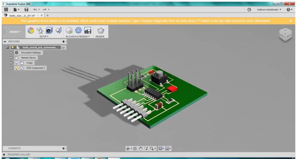
RENDERING THE CIRCUIT
- When I started searching for the way to render circuits created in Eagle, I found mainly 2 ways:
- Method 1 - Rendering using the new "FUSION SYNC" feature in Autodesk Eagle.
- Method 2 - Rendering using Eagle 3D and POV-RAY.
- I was really interested Method 1 (i.e: Using the FUSION SYNC) as it will also help me in my final project, so I started to do it using the following steps.
- Open the Eagle project where the Hello PCB circuit was created
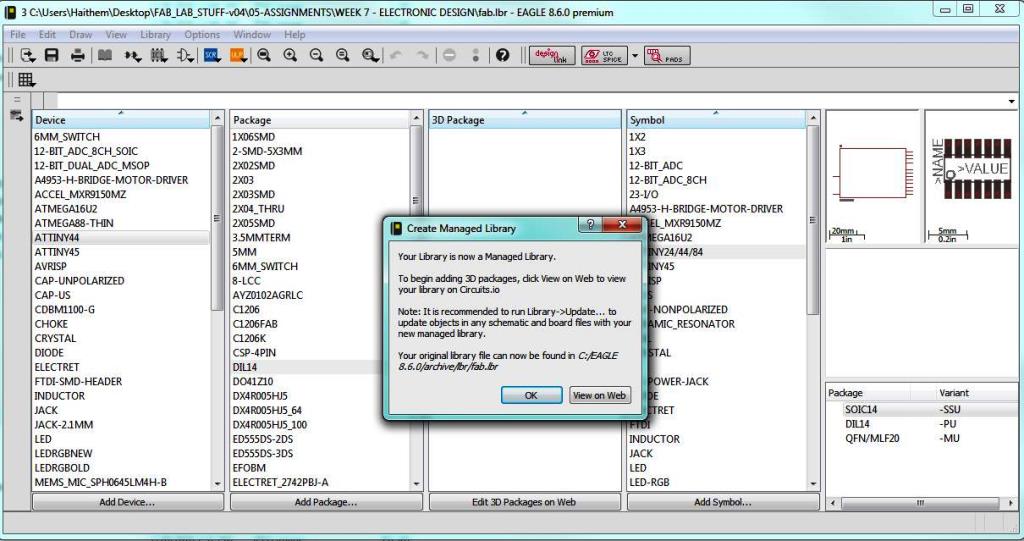
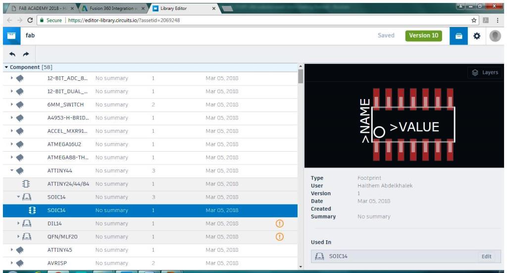
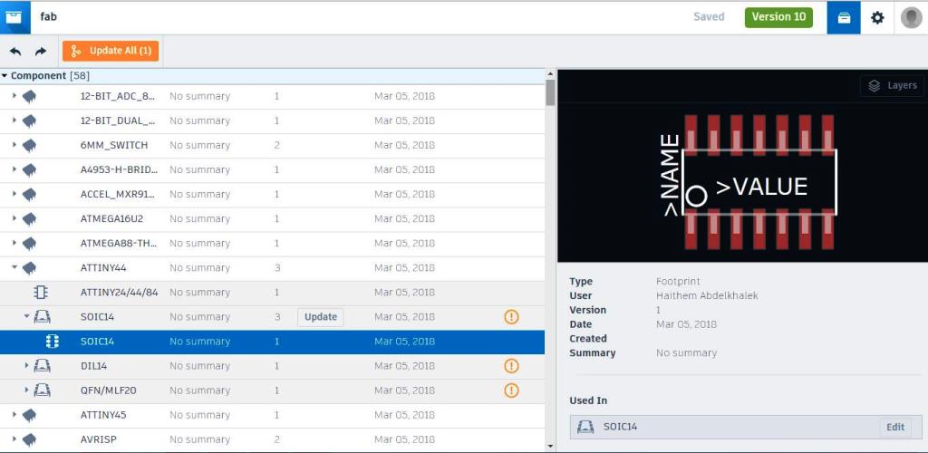
- Go Fab Eagle Library and open it. The library components does not have 3D packages, click on the "edit 3D packages on the web" button and accept to convert the library to a managed library then open THIS LINK to edit the library on the web.
- From the left side list browse till you reach the component you want to add 3D package for, then click the "Edit" from the right
- I was really interested in the first method (i.e: Using the FUSION SYNC) as it will also help me in my final project, so I started to do it using the following steps. I wenth through THIS TUTORIAL and THIS VIDEO which were so helpful
- Open the Eagle project where the Hello PCB circuit was created
- Go Fab Eagle Library and open it. The library components does not have 3D packages, click on the "edit 3D packages on the web" button and accept to convert the library to a managed library then open THIS LINK to edit the library on the web.
- From the left side list browse till you reach the component you want to add 3D package for, then click the "Edit" from the right side
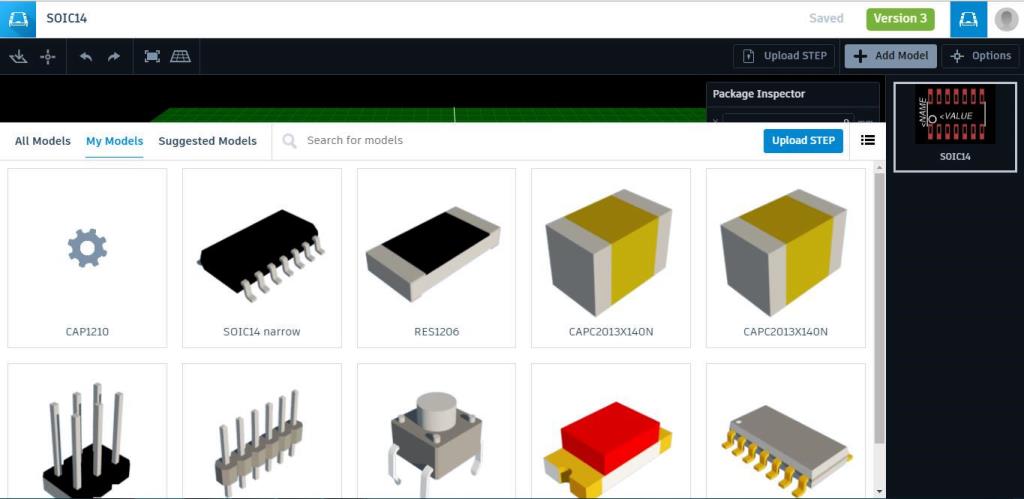
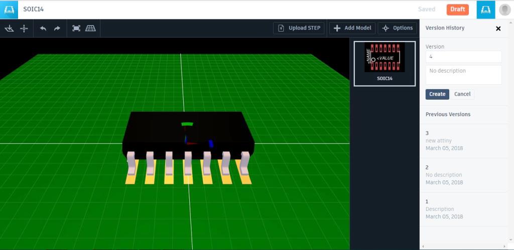
- Click "Add model" and select from suggested models the 3D package that suits your component, then click "DRAFT", dd a name and then "CREATE VERSION"
- In the library web page click "Update All"
- Do the same steps to add 3D packages to all the components in the library that exist in the PCB you want to render.
- Open Fusion 360 and create a new project to be ready to sync with the Eagle.
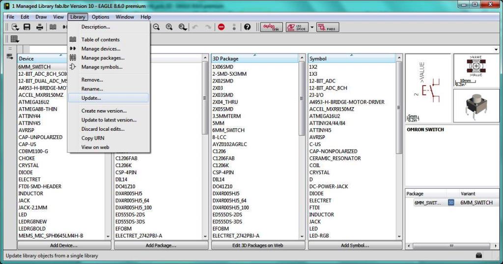
- Go Back to Eagle, Open the Fab Eagle library and click Update to ensure that the changes are reflected in the circuit you have created.
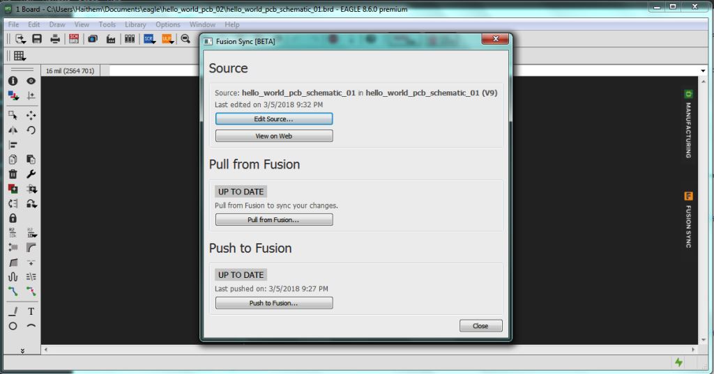
- Go to the board view and click "Fusion Sync", Select existing project (the fusion project you already created.
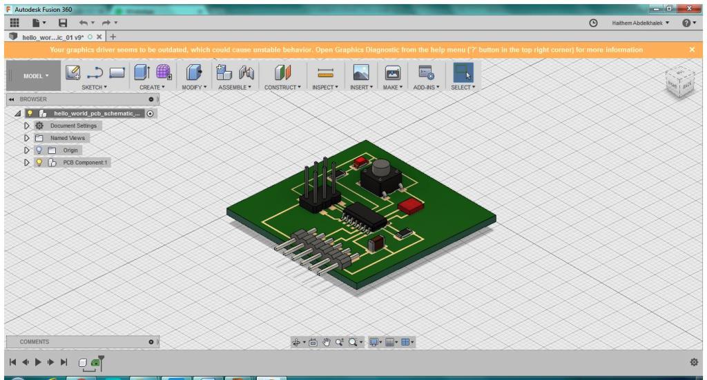
- Now Open Fusion and look at board and start rendering it.
Files: