FINAL PROJECT
WHAT IS MY PROJECT?
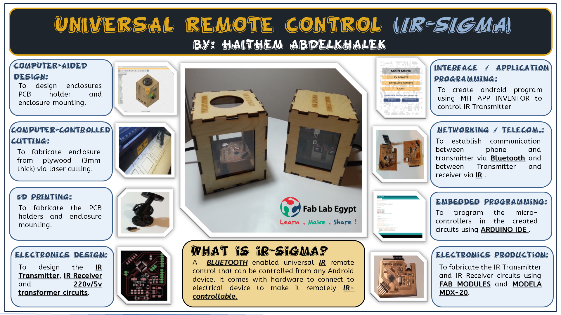
My project (Refered to here as IR-SIGMA) is a BLUETOOTH enabled universal IR remote control that can be controlled from any Android device (Referred to in this page as UNIT A). It also comes with an additional hardware (Referred to in this page as UNIT B) that can be attached / plugged to electrical device to make it IR remotely controllable (Example: can be switched ON and OFF)
WHAT WILL IT DO?
- The user choose a button with IR signal code and protocol from the Android application interface and then Push the button
- The IR Code is sent to the UNIT A (IR TRansmitter HUB) via Bluetooth.
- The IR Transmitter sends the IR Signal to the desired device.
- If the Transmitted IR Signal matches the one preset to UNIT B (IR Reciever) it stimulate a relay to TURN ON or TURN OFF the device it is attached to.
What I have in mind is that it should enable the user to remotely control several devices (even the ones that were earlier not remotely controllable) through UNIT A (Infra-red Transmitter Hub) and UNIT B (Infra-red Receiver) using a single easy to use android application interface as follows:
WHO HAS DONE WHAT BEFOREHAND?
When I did surf on the internet to look at similar devices, I did not find an exact match as most of the devices I found are designed to handle ONLY specific brands and the application associated with their commercial products is mainly to setup the the universal remote control rather than to operate it, below is a list of some similar end products that I found :
WHAT MATERIALS AND COMPONENTS WILL BE REQUIRED?
FROM WHERE?
HOW MUCH WILL IT COST?
The materials that that will be needed to fabricate the proposed project, the location from where it will be acquired and its cost will be 23.01 USD as below:
| # | COMPONENT | COUNT | UNIT PRICE | TOTAL PRICE | VENDOR | URL | NOTES |
|---|---|---|---|---|---|---|---|
| 1 | ATMEGA 328P-AU Micro-controller | 2 | 2.20 USD | 4.40 USD | FARNELL | LINK | |
| 2 | Crystal 16Mhz/18pF | 2 | 0.25 USD USD | 0.50 USD | FARNELL | LINK | |
| 3 | Green LED | 2 | 0.25 USD USD | 0.50 USD | FARNELL | LINK | |
| 4 | Red LED | 2 | 0.25 USD USD | 0.50 USD | FARNELL | LINK | |
| 5 | 10K Ohm Resistor | 2 | 0.05 USD | 0.1 USD | FARNELL | LINK | |
| 6 | 499 Ohm Resistor | 2 | 0.05 USD | 0.1 USD | FARNELL | LINK | |
| 7 | 22 Pf Capacitor | 4 | 0.1 USD | 0.4 USD | FARNELL | LINK | |
| 8 | 1K Ohm Resistor | 8 | 0.1 USD | 0.8 USD | Digi-Key | LINK | |
| 9 | FTDI Header | 2 | 0.25 USD | 0.5 USD | FARNELL | LINK | |
| 10 | Phototransistor IR | 1 | 0.41 USD | 0.41 USD | Digi-Key | LINK | |
| 11 | HC-05 Bluetooth Module | 1 | 7.5 USD | 7.5 USD | Hilegto | LINK | |
| 12 | IR Transmitter LED | 1 | 0.05 USD | 0.05 USD | RAM(LOCAL SHOP) | LINK | |
| 13 | IR receiver | 1 | 0.35 USD | 0.35 USD | RAM(LOCAL SHOP) | LINK | |
| 14 | 220v to 5v module | 1 | 3.5 USD | 3.5 USD | RAM(LOCAL SHOP) | LINK | |
| 15 | Solid State Relay | 1 | 3.4 USD | 3.4 USD | RAM(LOCAL SHOP) | LINK |
WHAT PROCESS WILL BE USED?
| # | TASKS | PROCESS |
|---|---|---|
| IR TRANSMITTER (UNIT A) | ||
| 1 | Design Enclosure Using Autodesk Fusion 360. | Computer-Aided Design |
| 2 | Design Enclosure Accessories (PCB-Holders). | Computer-Aided Design |
| 3 | Fabricate the Enclosure Using laser cutter. | Computer-Controlled Cutting |
| 4 | Fabricate Enclosure Accessories (PCB-Holders). | 3D Printing |
| 5 | Circuit Design using Eagle. | Electronics Design |
| 6 | Produce the Electronic PCB. | Electronics Production |
| 7 | Program the Board. | Embedded Programming |
| IR RECEIVER (UNIT B) | ||
| 8 | Design Enclosure Using Autodesk Fusion 360. | Computer-Aided Design |
| 8 | Design Enclosure Accessories (PCB-Mounting Kit). | Computer-Aided Design |
| 9 | Fabricate the Enclosure Using laser cutter. | Computer-Controlled Cutting |
| 10 | Fabricate Enclosure Accessories (PCB-Mounting Kit). | 3D Printing |
| 11 | Circuit Design using Eagle. | Electronics Design |
| 12 | Produce the Electronic PCB. | Electronics Production |
| 13 | Program the Board. | Embedded Programming |
| ANDROID APPLICATION INTERFACE | ||
| 14 | Design application User Interface using MIT App Inventor. | User Interface (GUI) |
| 15 | Coding and Testing Application. | User Interface (GUI) |
| INTEGRATION, ASSEMBLY AND DOCUMENTATION | ||
| 16 | Integrate All parts and Systems. | All Above |
ENCLOSURE (CHASSIS) DESIGN AND FABRICATION:
ENCLOSURE DESIGN
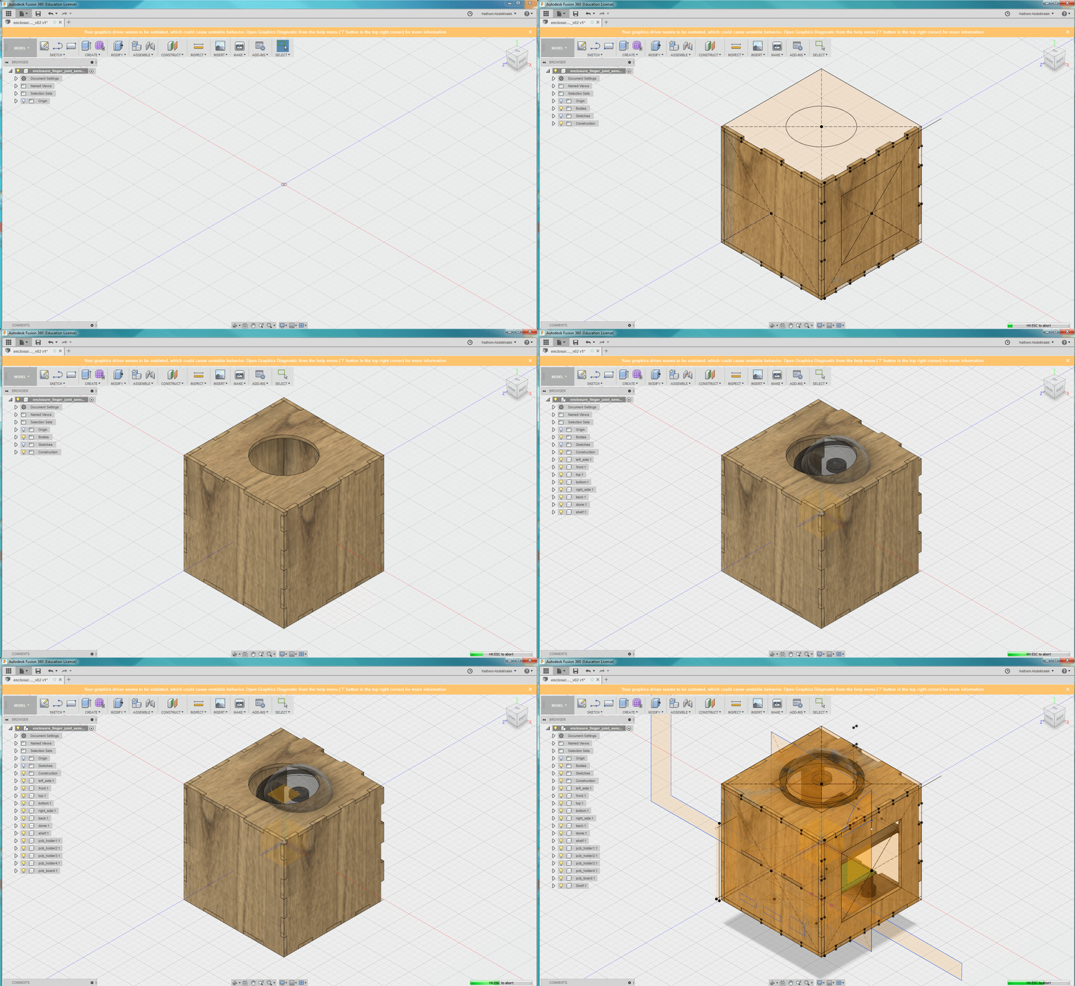
- For the enclosure design, I decided to use the Autodesk Fusion 360. I started with the parametric press-fit box I designed in WEEK2, All the steps for the design of the press-fir box are listed in THIS PAGE .
- To create a CUBE (10 CM x 10 CM x 10 CM), I modified the (LENGTH x WIDTH x HEIGHT) Parameters to be all equal to 10 CM.
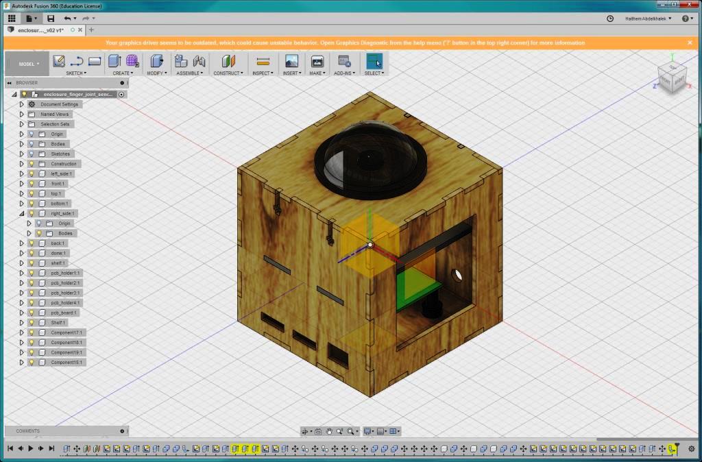
- I performed the following modifications to the original design:
- I cut a square opening through the front and back faces, this is to ensure that I will have a clear view of the PCB later and for the IR emmitter and receivers to have an open view / space for IR transmissions.
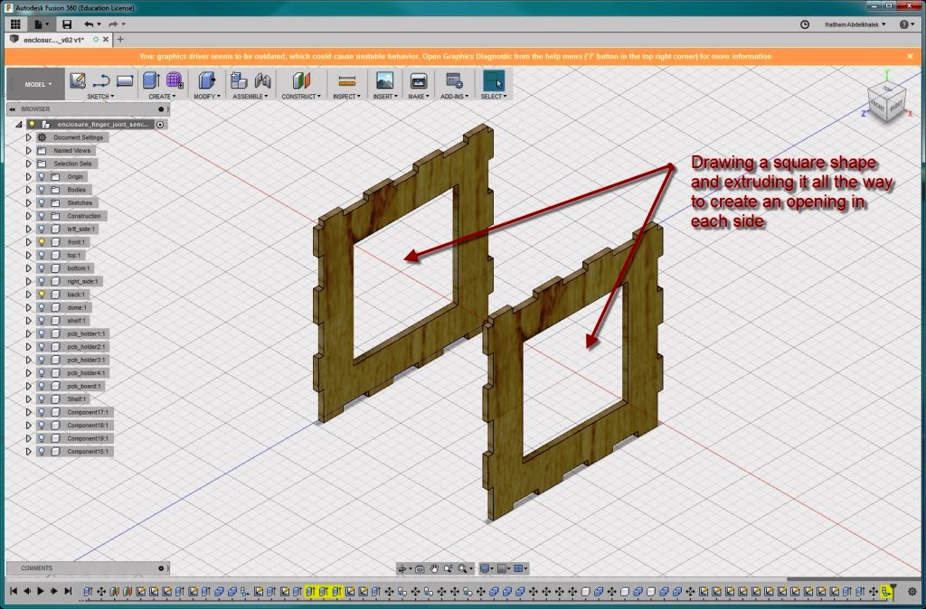
- On Side A: I cut openings for the FTDI cables, BLUETOOTH connector and USB power connector.
- On Side B: I cut openings for the POWER IN and POWER OUT cables (Will ONLY be used in RECEIVER UNIT - refered to in this document as UNIT B).
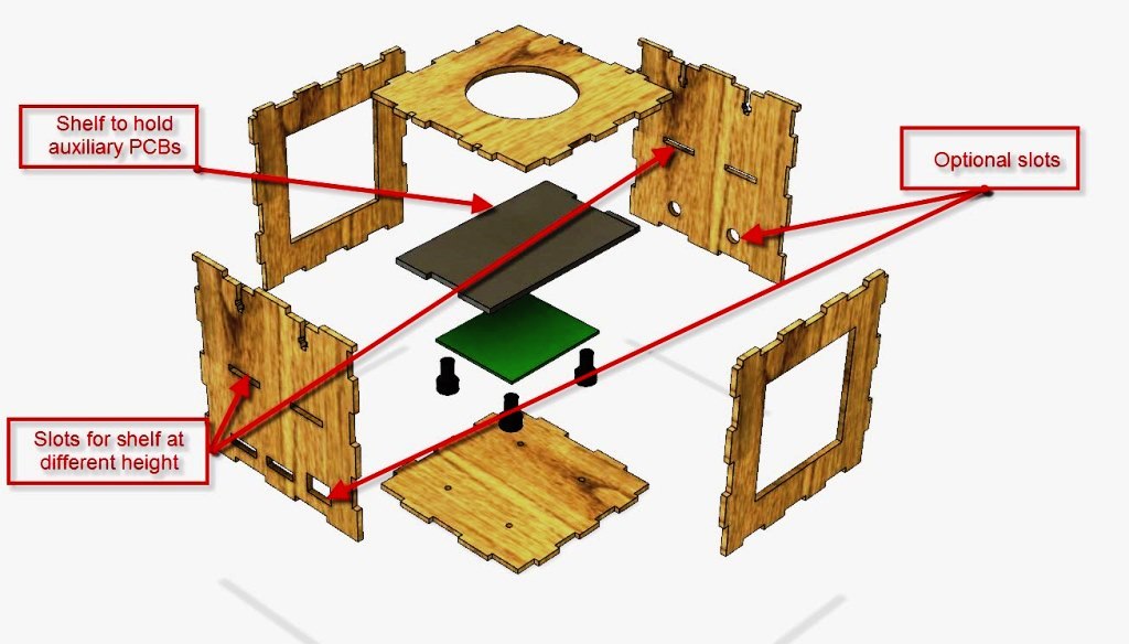
- On Sides A and B: I cut through slots for shelf at 2 different levels to ensure that I can add a shelf for secondary circuit later and adjust the shelf height.
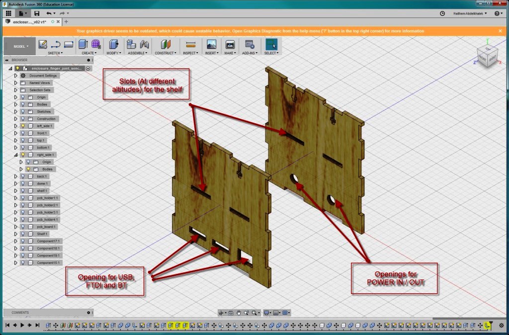
- The final enclosure design looked like the image below.
- I then exported the faces of the enclosure to DXF files.
In my design I thought of the following considerations that proved to be useful later as follows:
- I intend to have 2 devices (refered to as UNIT A and UNIT B) but instead of creating 2 enclosures, I created ONE enclosure design that will fit for both devices. I added optional openings and slots that can be used in one and might not be needed in the other. The reason behind that is to: SAVE COST, MAXIMIZE USAGE and SIMPLICITY .
- I added a shelf in my enclosure to give me the luxury of adding additional auxiliary PCB boards or to help in organizing the cables.
- Since in that stage I did not know the height of the components in my circuit and I added slots for the shelf at 2 different altitudes to enable mounting the shelf at 2 different heights.
ENCLOSURE FABRICATION
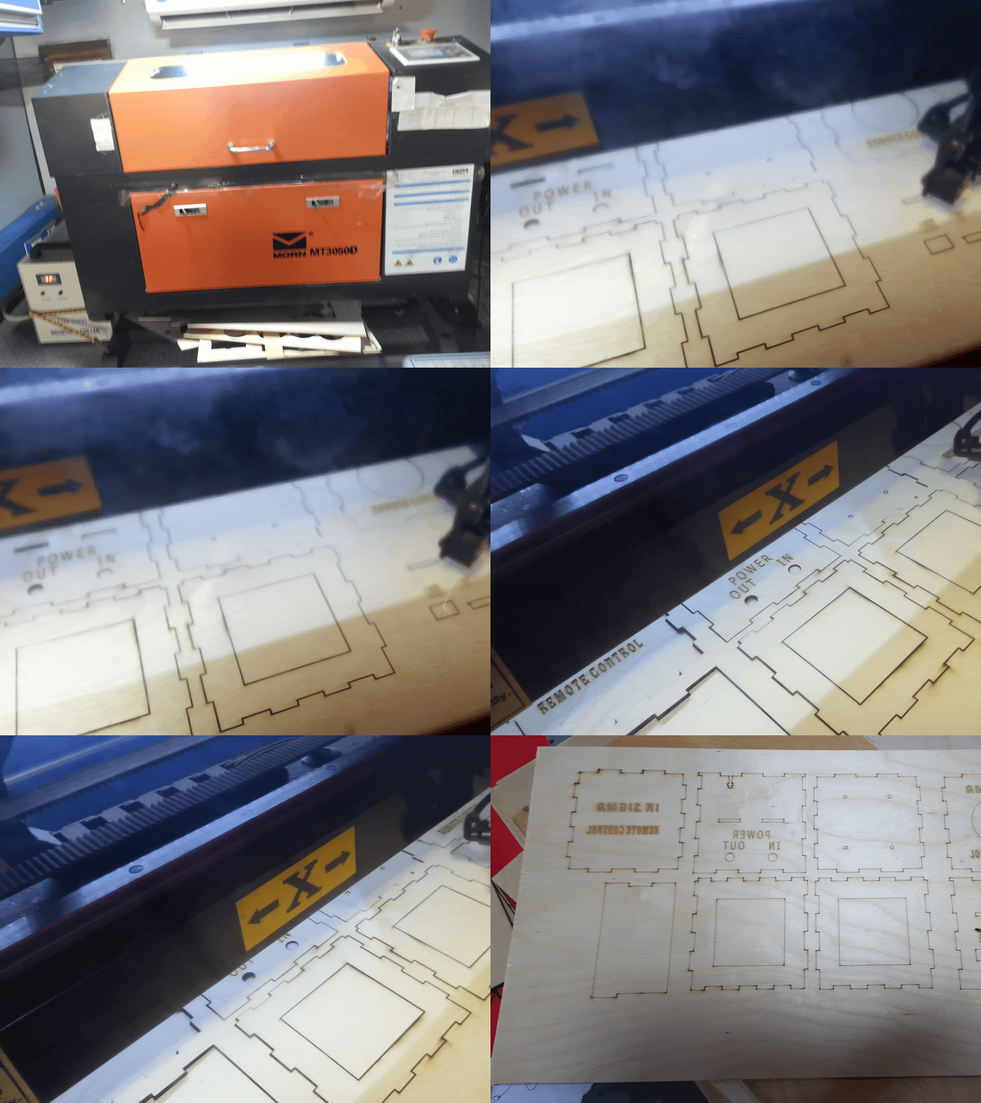
- I decided to use plywood (3 mm Thickness) to create my enclosure and to cut it using the laser cutter we have in the lab MORN MT3050D.
- I followed the same steps listed in WEEK4
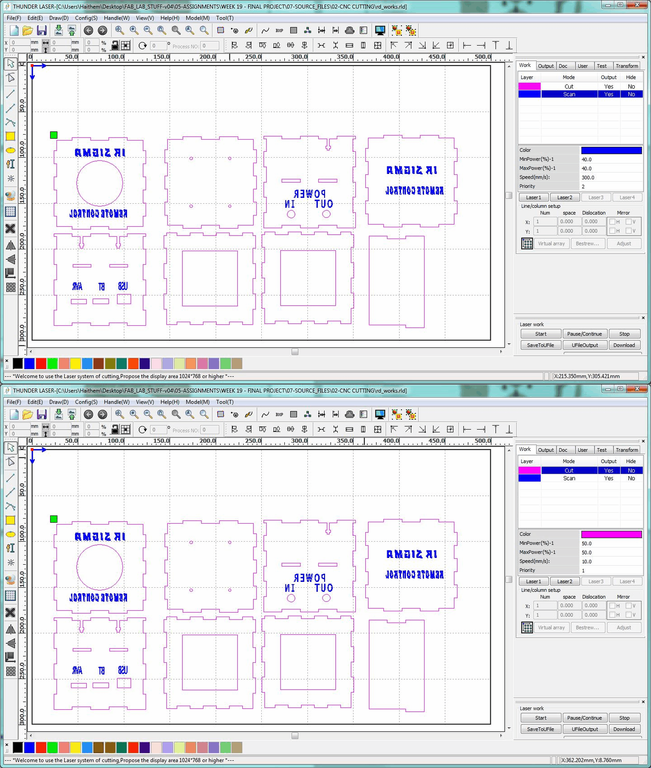
- I imported the DXF files that were exported earlier in Autodesk Fusion 360 and I added text to label openings in the enclosure and to add the final product name (i.e: IR SIGMA)
I did put the text in the right orientation in the begining but I found that the resulting cut had the text reversed ... WHY?, the reason was that the origin in the laser cutter was on the top right where as the one in the RD works software was in the top left. so in short the Origin is REVERSED / MIRRORED. The work around for that was simply to reverse / mirror the text.
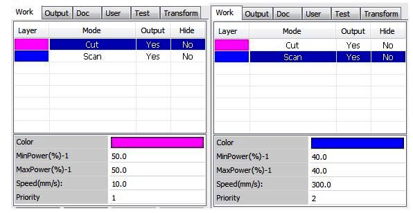
- I adjusted the Laser cutter SPEED and POWER as follows:
- For SCAN: POWER= 40% , SPEED= 300 mm/s.
- For CUT: POWER= 50% , SPEED= 10 mm/s.
- I started the cutting process
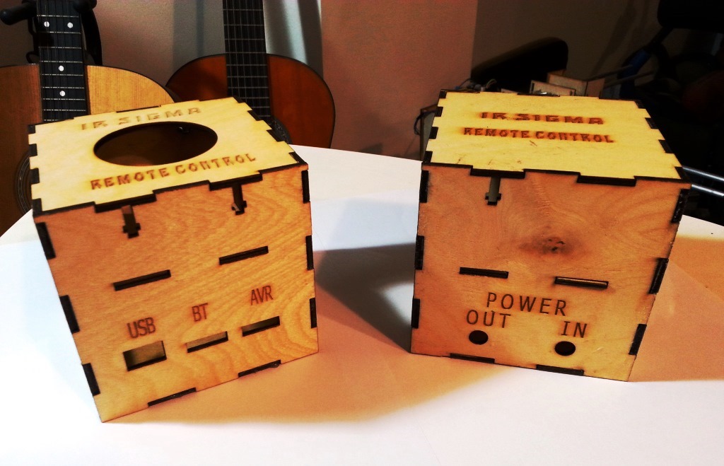
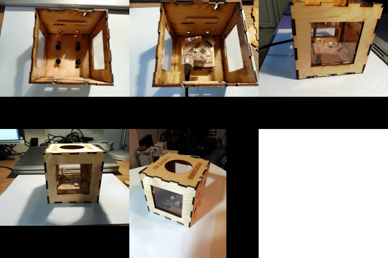
- I assembled the cut parts and the result is as shown below
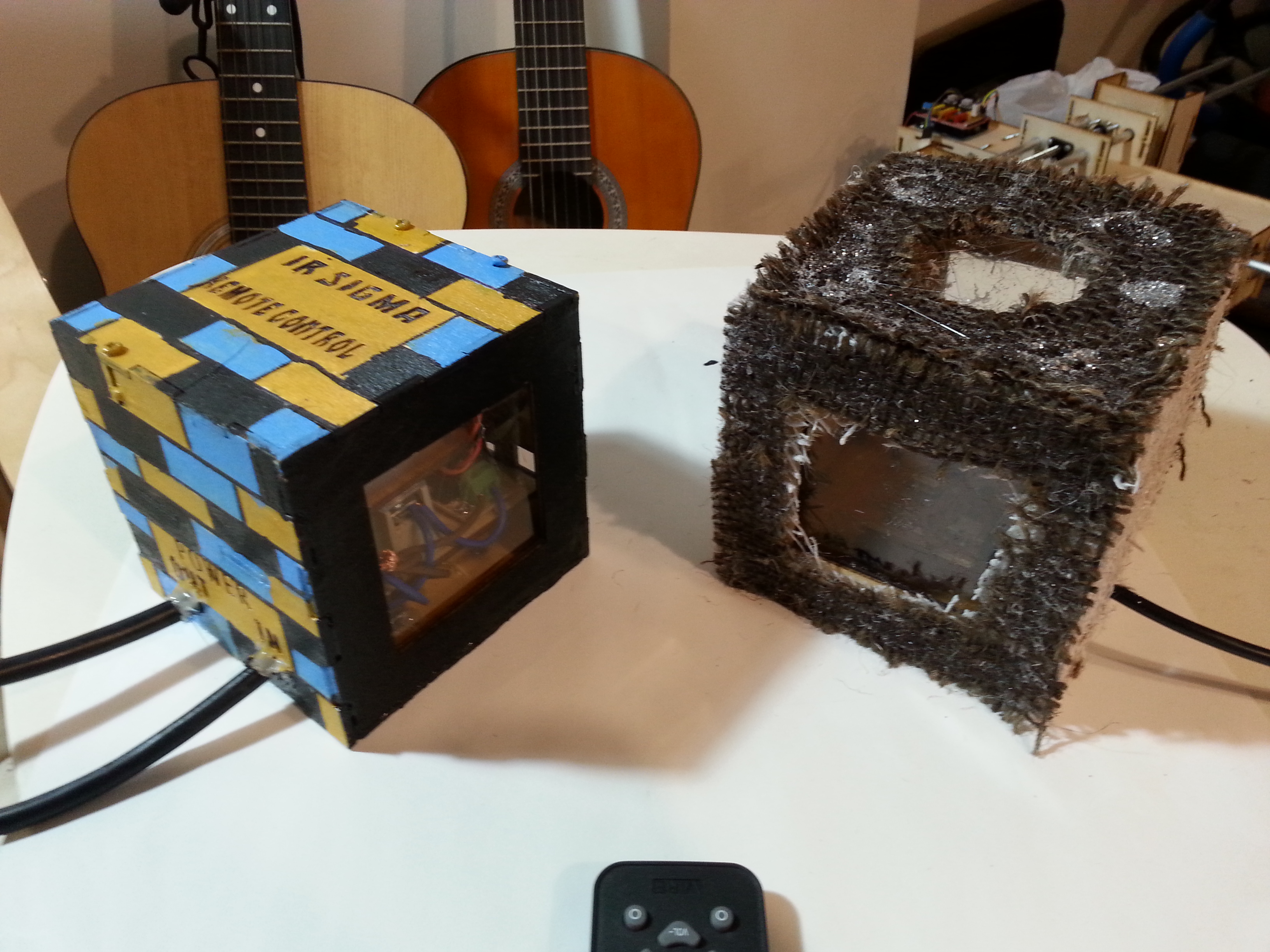
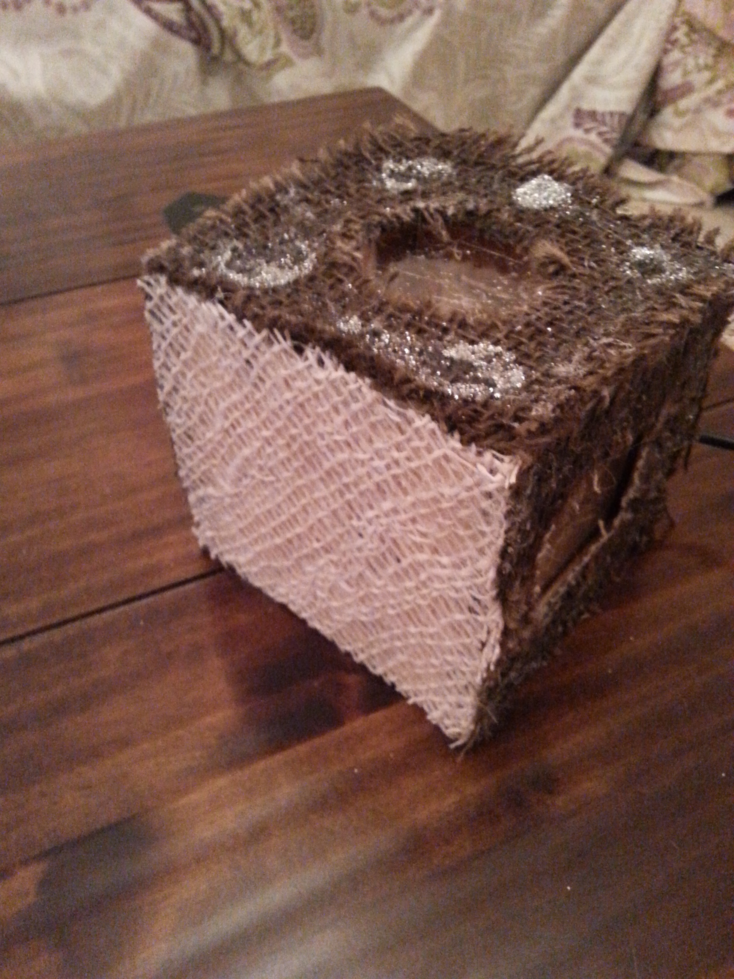
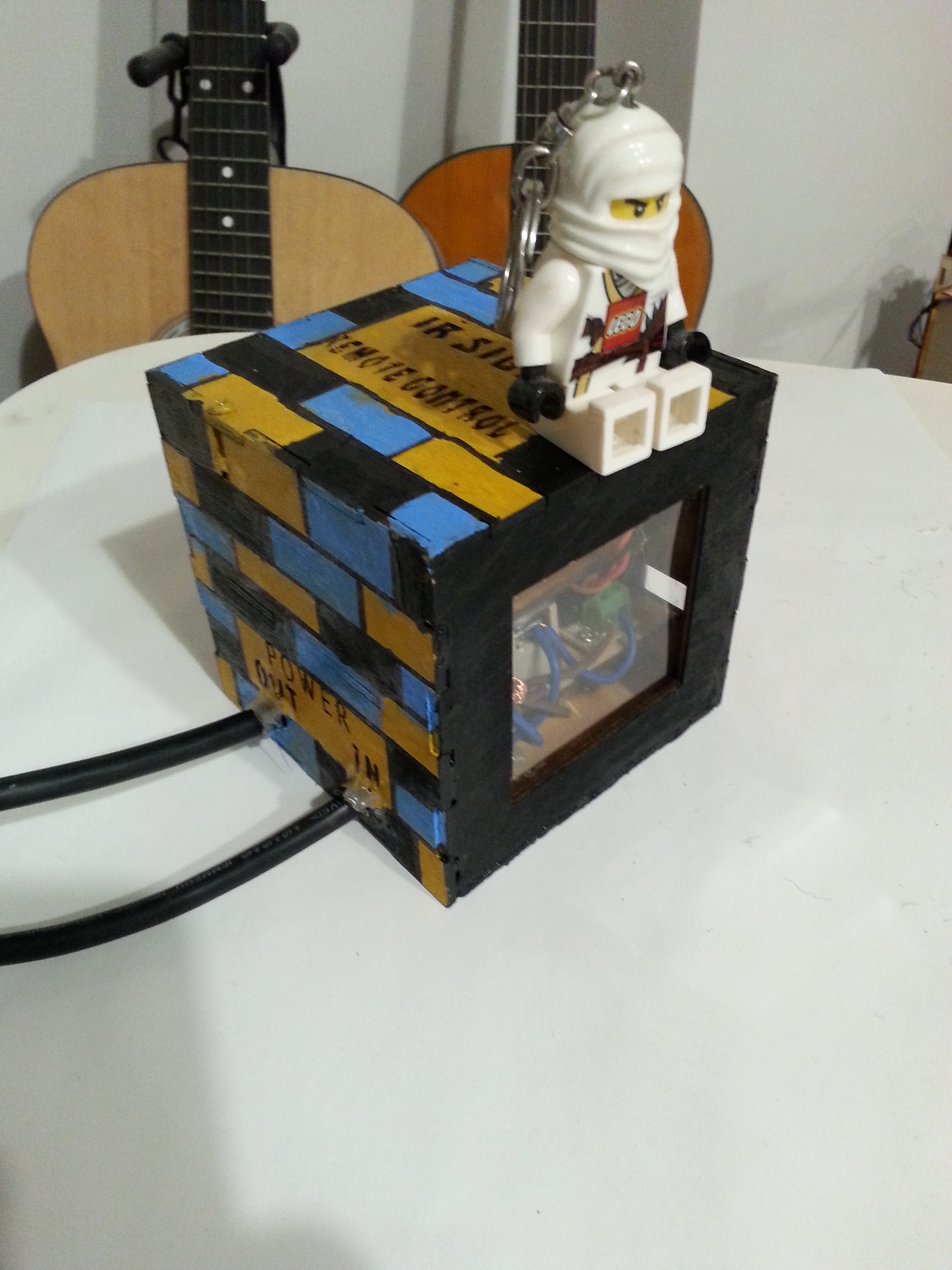
I was told ONLY 48 hours before the presentation scheduled day (i.e: 13th June 2018, that I might get a comment that the enclosure is not attractive enough, I was also referred to THIS LINK. Well this was a very short notice for me to re-design the whole thing and although for me this is a proto-type and a prof of concept and will not be intended to be the version that I will distribute as an end product but I decided to give it a try and make it more attractive. I did the following two versions:
- The first version (might suit my living room) I covered the enclosure with canvas cloth and I covered different layers with hot wax and here we are with an enclosure that is WATER PROOF. Is that an application of composites!?
- In the second version (might match my kids room) I painted the enclosure with a tile style using the same colors that I used in my website theme.
ENCLOSURE ACCESSORIES (PCB HOLDER AND MOUNTING KIT) DESIGN AND FABRICATION:
ACCESSORIES DESIGN
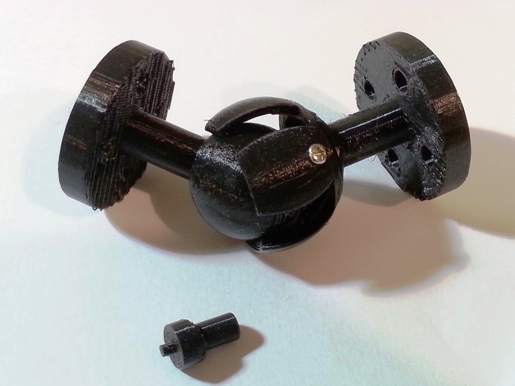
- For UNIT B (THE RECEIVER) I decided to create a ball hinge to mount the enclosure to ensure that it can be mounted in a place where UNIT A (THE TRANSMITTER) can establish a line of sight with.
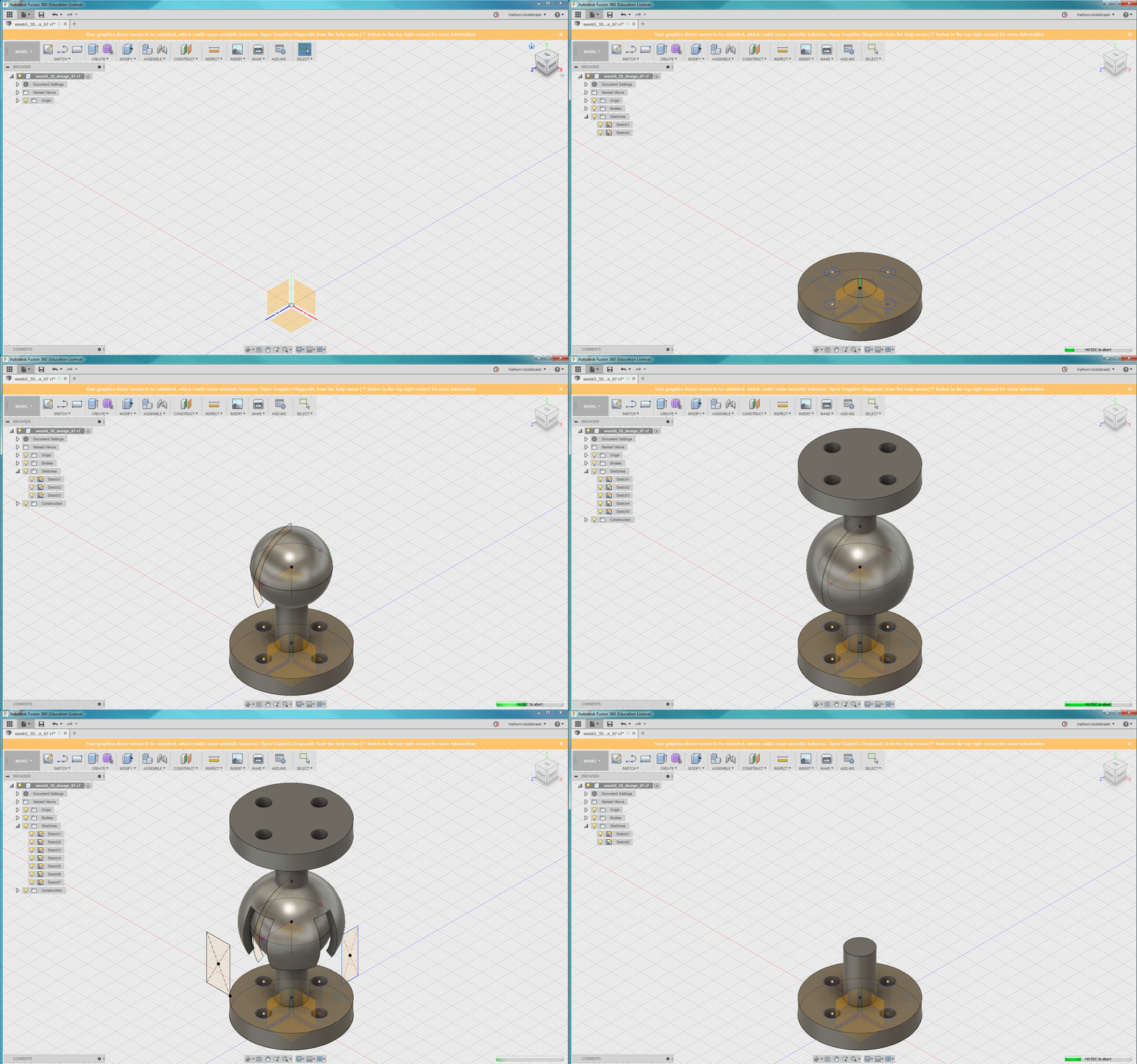
- I used Autodesk Fusion 360 to create my design, I created a new design project and I performed the following steps:
- I created a new sketch where I did draw a circular base and extruded it.
- I then sketched the holes for mounting screws in the base and the rod extruded out from the base.
- I then draw a circle and revolved it to create a ball.
- Then I draw an arc and revovled it to create the top circular part of the ball hinge. and extruded from it the top rod.
- Finally I sketched a rectangle and cut through the top circular part of the hinge.
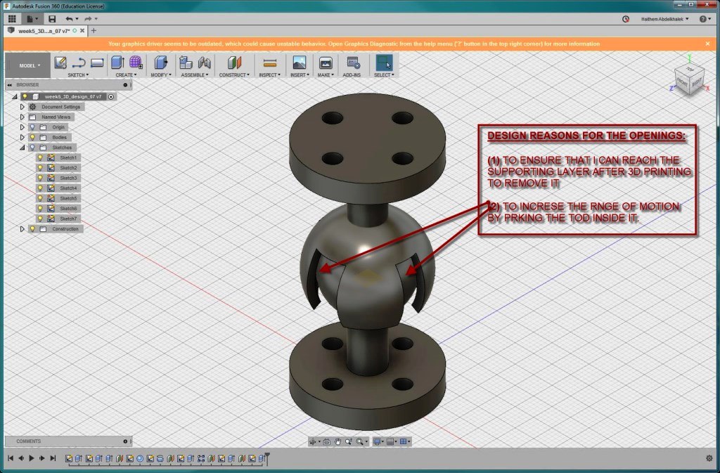
- To ensure that I will have access to remove the supporting layers after I 3D print the hinge.
- To increase the range of motion of the rod in the bottom sphere by allowing the rod to park inside the slot.
There are TWO RESASONS why I created the slots in the top sphere in the ball hinge as shown in the image below:
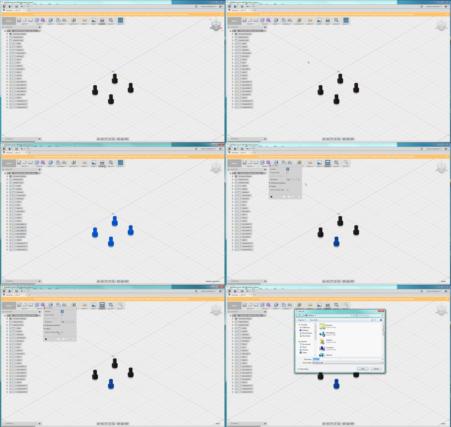
- Finally I exported the hinge as STL files, I also exported the PCB holders from the Enclosure Fusion project.
ACCESSORIES FABRICATION
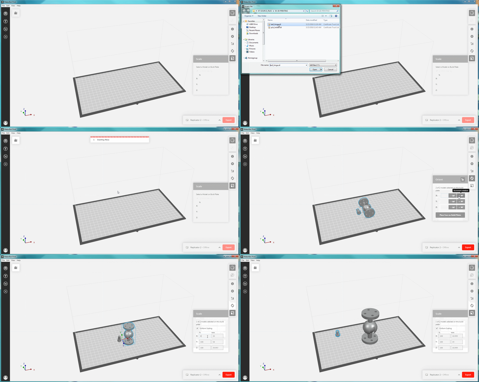
- Now it is time to 3D print the accessories parts, I used MAKERBOT and I used the same methodology stated in WEEK 6 assignment.
- I opened MAKERBOT software and I imported the 2 STL files I exported Earlier and existing HERE and HERE
- I then left everything to the default and modified the following configuration ONLY:
- I increased the support Density from 15% to 20% (Why?.. Because the ball hinge is having weight and to make sure the support will hold it)
- I increased the infill desnsity from 15% to 20% (Why?.. to ensure the ball hinge is tough enough and will not break)
- I then exported the file to a memory SD card to put it in the 3D printer and print it.
ELECTRONIC CIRCUITS (PCB) DESIGN AND FABRICATION:
ELECTRONIC CIRCUITS DESIGN
- I used the same methods and techniques learned in WEEK 7 to design my electronic circuits.
- I needed to design 4 circuits for my project as follows:
- PCB for UNIT A (IR Transmitter) and UNIT B (IR Receiver), I used the same design for both circuits.
- PCB for 220 volts AC to 5 volts DC step down module.
- PCB for IR Emmiter.
- PCB for IR Receiver.
MAIN UNIT A / UNIT B PCB DESIGN:
- I realized in early stages that the program that I will need to upload to my microcontroller WILL NOT FIT in ATTINY 44 or ATTINY 45 because:
- It needs programming memory way above the 4k limit available for the ATTINY Series.
- It will need to use the Arduino IRremote library that is will suited and created for the arduino ATMEGA 328 Microcontroller.
- Accordingly I decided to use the ATMEGA 328-PU, more about the ATMEGA 328-PU can be found from THIS DATASHEET.
- In order not to re-invent the wheel, started with the satsha-kit design and I modified it to remove un-needed pins and add my components.
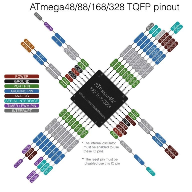
- I went through the IRremote arduino linrary to know which arduino pins I will use and I used the diagram below that showed the ARDUINO PINS corresponding to each ATMEGA 328-PU PINS, finally I decided to connect the following pins:
- IR Transmitter PIN = ARDUINO PIN 3 -> ATMEGA 328P PCINT 19
- IR RECEIVER PIN = ARDUINO PIN 11 -> ATMEGA 328P PCINT 3
- BLUETOOTH TX PIN = ARDUINO PIN 10 -> ATMEGA 328P PCINT 2
- BLUETOOTH RX PIN = ARDUINO PIN 09 -> ATMEGA 328P PCINT 1
- I used Eagle and I created the following schematic and board as below:
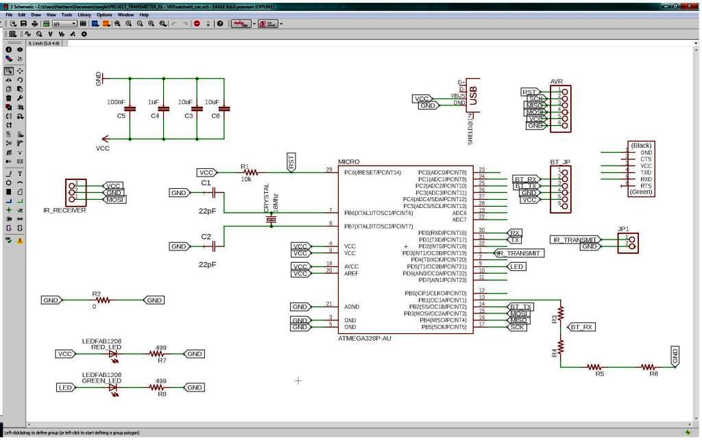
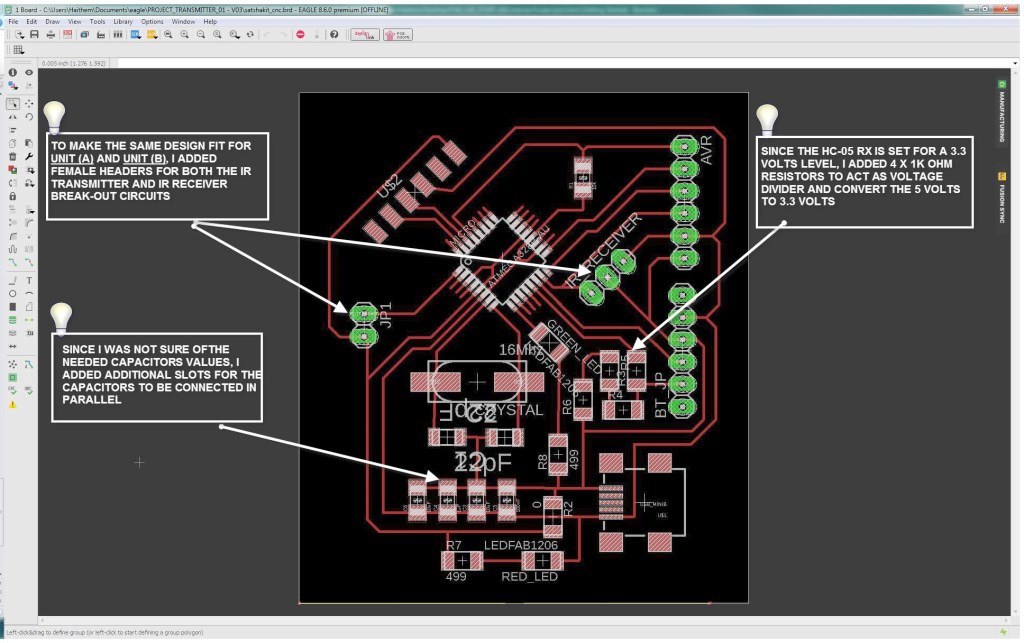
-
DESIGN TIPS AND CONSIDERATIONS:
In this PCB design I considered the following in my design:
- I made 1 PCB design that will fit both the UNIT A and UNIT B by simply adding female headers for both the IR emmiter and Receiver in each of the 2 boards. this will save the efforts to create 2 different boards and provide excahnge-ability as well as the spare ports / female headers proved to be usefull in case I need to add more functionality to the PCB board later on.
- I was not sure of the amount of the needed capacitance so I added additional pads to connect additional capacitors on parallel.
- I knew that I will use later HC-05 module and since its RX pin work on a voltage level of 3.3 volts instead of the 5 volts, I created a voltage divider bridge using 4 x 1 K ohm resistors to get 3.3 volts out of the 5 volts coming out from the ATMEGA 328PU pins.
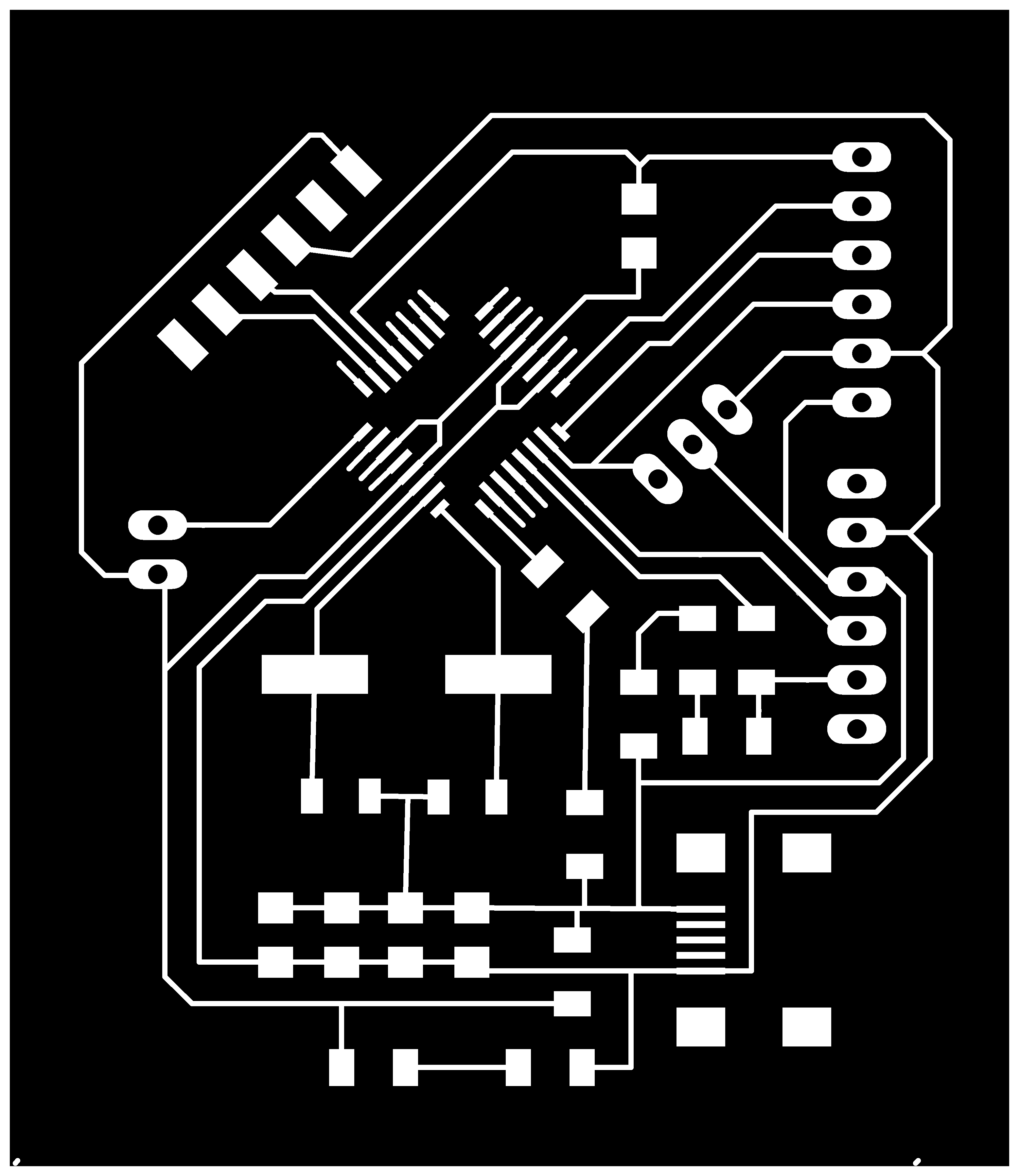
- I then exported the traces and outlines PNG files below and I edited them using GIMP using the same methods I documented in WEEK 7.
-

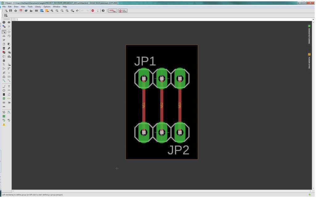
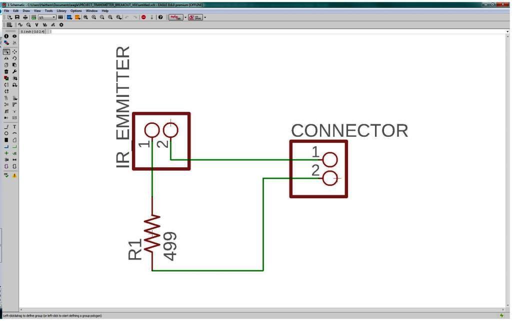
IR EMMITTER AND RECEIVER BREAKOUT PCB:
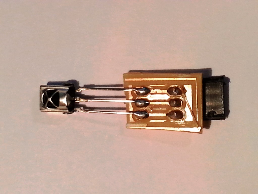
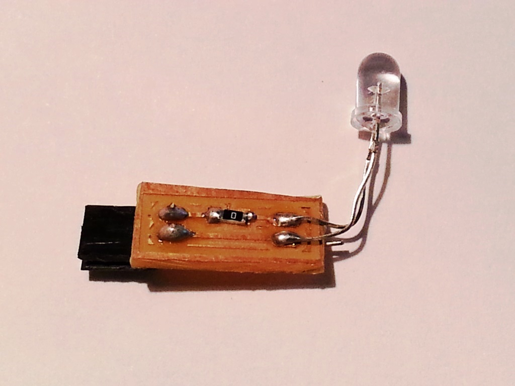
- To avoid ending up with too many jumper cables and to elevate the emmitter above th level of the pcb to ensure that the IR beam will have line of sight to transmit or receive. I decided to create a breakout PCB (i.e: a PCB that has the IR transmitter and receiver and connected to the main PCB with FEMAL-HEADERS)
- I used Eagle and I created the following schematics and boards as follows:
-
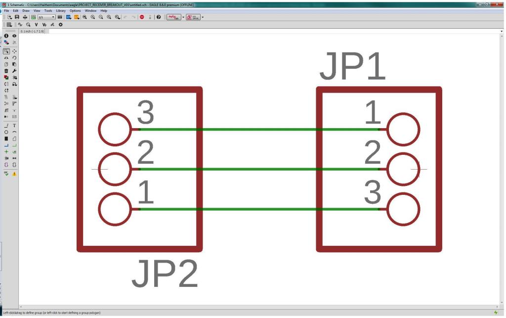
-
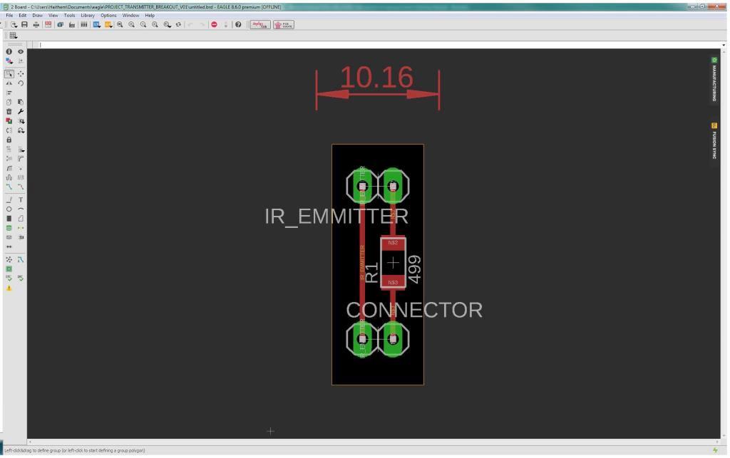
-
- I then exported the traces and outlines PNG files below and I edited them using GIMP using the same methods I documented in WEEK 7.
-


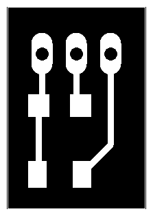


220 VOLTS AC TO 5 VOLTS DC MODULE PCB:
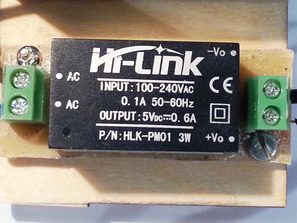
- For UNIT B (The IR Receiver): The UNIT B will be connected to a device (Example: a lamp) which will usually get 220 volts input, Instead of using 2 power input (220 volts AC one for the lamp and 5 Volts DC one for for my UNIT B board), I decided to use 220 Volts AC to 5 volts DC module so that I can SINLE POWER-IN .
- I decided to use a module named HLK-PM01 whch can be obtained locally from HERE , more about the module can be found from THIS DATASHEET.
- I used Eagle and I created the following schematic and board as follows:
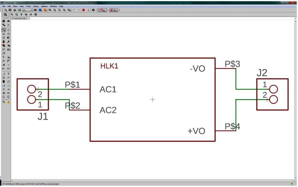
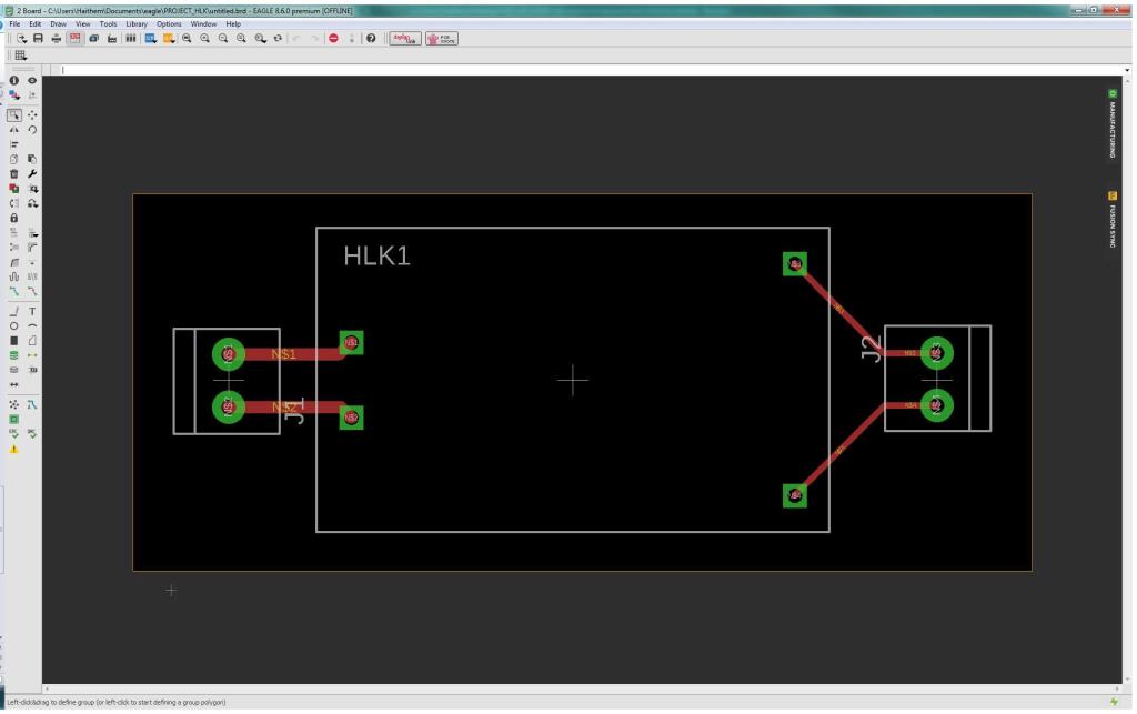
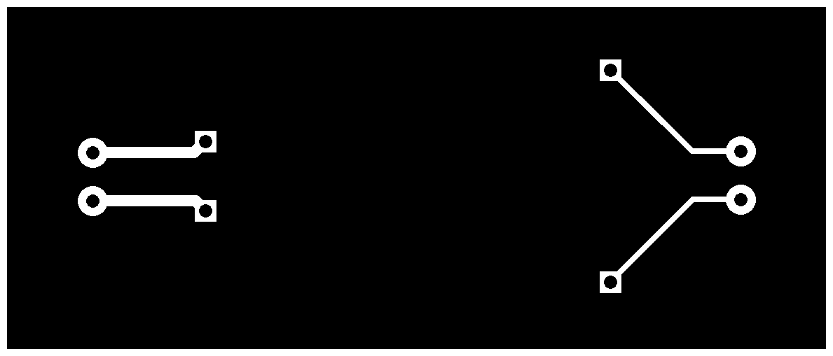
- I then exported the traces and outlines PNG files below and I edited them using GIMP using the same methods I documented in WEEK 7.
-

-
WHY TO HAVE 220 VOLTS AC INPUT SOURCE IN A SEPARATE PCB?
In this PCB design the main reasons to put the 220 Volts AC input in a separate PCB are:
- In the context of power supply design, isolation is the electrical and sometimes magnetic separation between two circuits in close proximity to each other..
- Main Purposes of Power Supply Isolation: There may be many purposes for isolation but in our case the most important ones are:
- Safety: Electronic power supplies commonly process dangerous voltages with low impedances. Isolation is often required to prevent contact with dangerous voltages. Transformers used within power supplies function as a safety isolation transformer.
- Voltage Level Shifting: Power supply designs must often accommodate loads at different potential voltages than the source.
- Power Supply Isolation Methods used:
- Physical Separation: The most obvious form of power supply isolation is simple physical separation — used when there is no electrical, magnetic, or thermal interaction desired. The separation may employ different types of dielectric mediums between the conducting surfaces.
- Transformers: Transformers provide electrical isolation, but allow power to be magnetically coupled through from primary to secondary. They are used when it is desired to transfer power across the power supply isolation boundary and can be designed for safety isolation, voltage level translation, step-up, step-down functions, and for obtaining multiple outputs.
ELECTRONIC CIRCUITS PRODUCTION
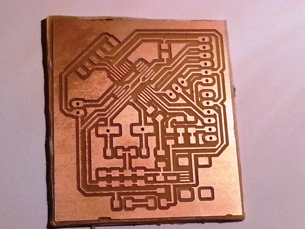
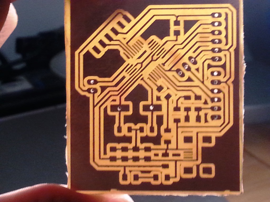
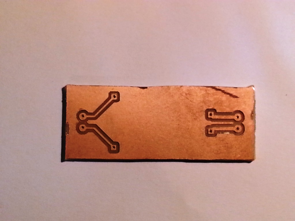
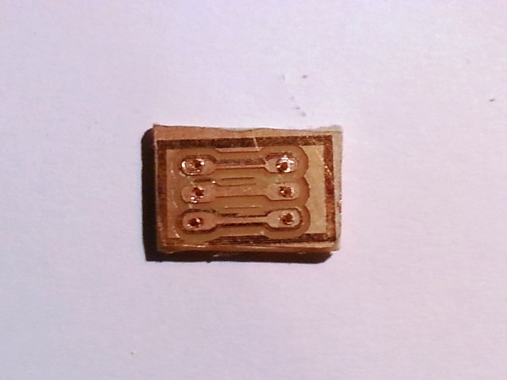
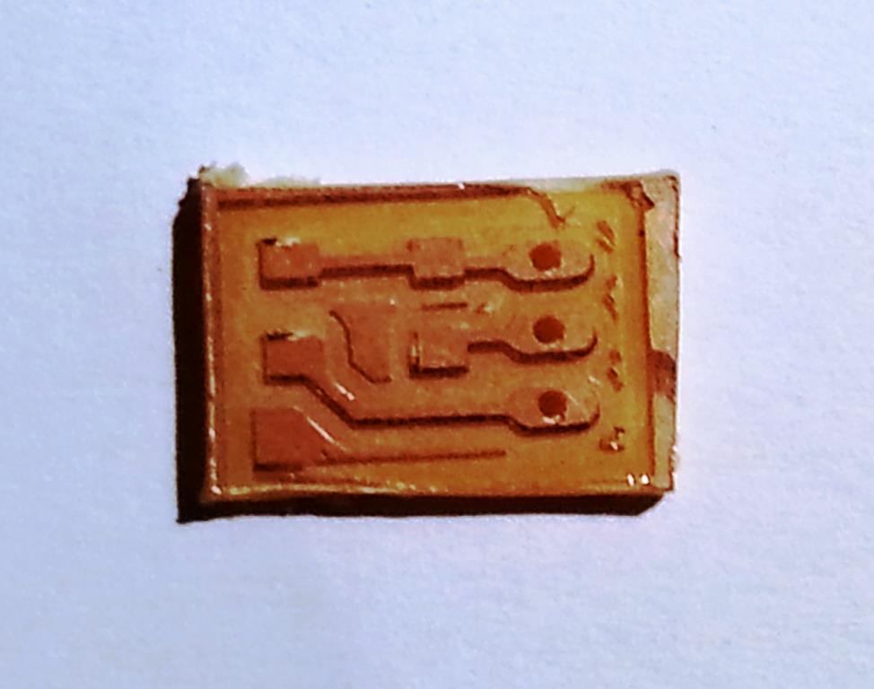
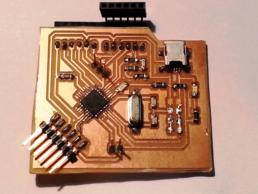
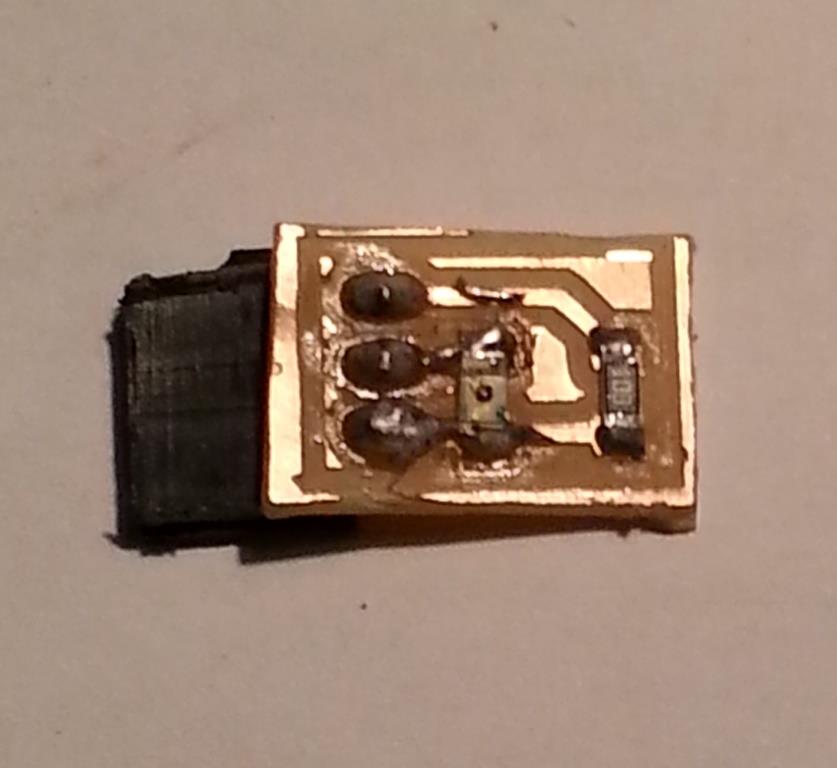
- Now it is time to CNC-mill the PCBs using MDX-20, I applied the same methods and techniques I documented earlier in WEEK 5
- I then created the boards shown in the images below.
- Then I soldered the different components in each PCB and the soldered boards are as shown below:
-
FABRICATION TIP: When I exported the PNG file to import it in Fab-modules, I initially exported it at 500 dpi but this led to errors and the traces of the ATMEGA 328 were not separated, the reason for that was the tilted position of the ATMEGA328 and accordingly the traces were diagonal lines. I resolved the issue by exporting to 1500 dpi and accordingly the image was with a higher resolution and could see the traces separated.
PROGRAMMING THE MICROCONTROLLERS (EMBEDDED PROGRAMMING):
In this section I will document 2 embedded programs since I have TWO ATMEGA micrcintrollers on 2 seaprate PCB boards, In the programming there are common facts that applies to both my programs as follows:
- I will use ARDUINO IDE to program both microcontrollers.
- I will use an ARDUINO known library named "IRremote" to perform the IR TRANSMIT and IR RECEIVE functions in the code, the IRremote library can be downloaded from HERE, Also the IRremote library documentation can be found HERE.
For both boards perform the following Steps:
- Connect the Transmitter board to the FABISP programmer as shown below:
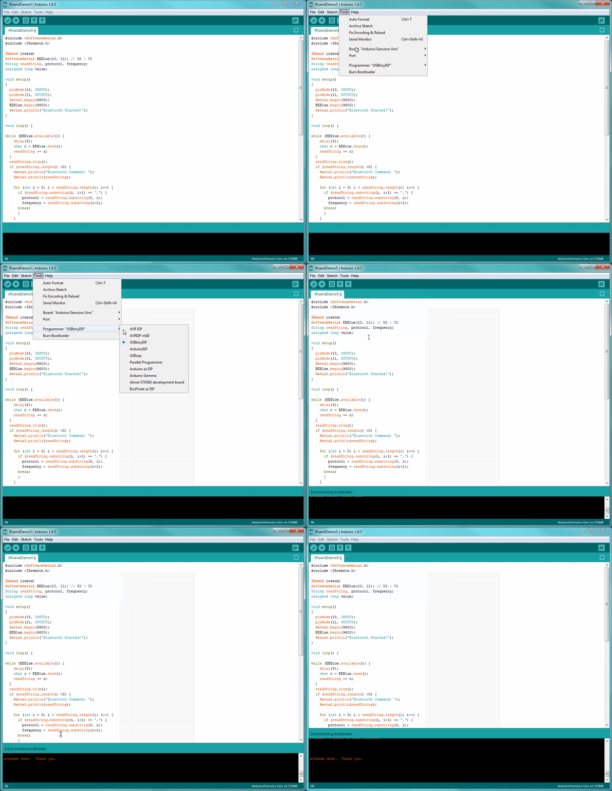
- In ARDUINO IDE: go to TOOLS menu -> choose the following and then press "BURN BOOTLOADER":
- Board = "ARDUINO / GENUINO UNO"
- Port = "PORT THE BOARD IS CONNECTED TO"
- Programmer = "USBIspTiny"
PROGRAMMING THE IR TRANSMITTER (UNIT A) MICROCONTROLLER
-
WHAT IS THE BOARD FUNCTION WE WANT TO IMPLEMENT?
The transmitter board needs to perform the following functionality:.
- Receive via connected HC-05 Bluetooth module the IR Protocol and IR Signal Code (In Hexa Decimal) combined in one string.
- Parse the received string and separate the Protocol from the IR Code.
- Check the protocol and for Each respective protocol value, use the corresponding suitable IRSEND function to transmit the IR code via the IR transmitting LED.
- I installed the "IRremote" Library: I unzipped the library file to a folder -> copeid the folder to "C:\program files\arduino\library"
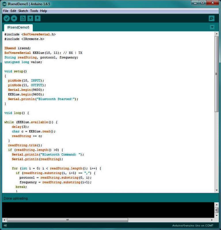
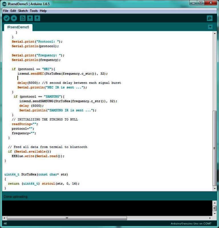
- I wrote the following code as shown below:
- Press "CTRL + SHIFT + U" to upload the code using the programmer
- I tested the functionality.
PROGRAMMING THE IR RECEIVER (UNIT B) MICROCONTROLLER
-
WHAT IS THE BOARD FUNCTION WE WANT TO IMPLEMENT?
The receiver board needs to perform the following functionality:.
- Receive via IR an IR code from UNIT A (IR Transmitter Hub).
- Compare the code to a PRE-SET code and if it matches it signal out a a HIGH on PIN 3 otherwise it signals LOW.
- I installed the "IRremote" Library: I unzipped the library file to a folder -> copied the folder to "C:\program files\arduino\library"
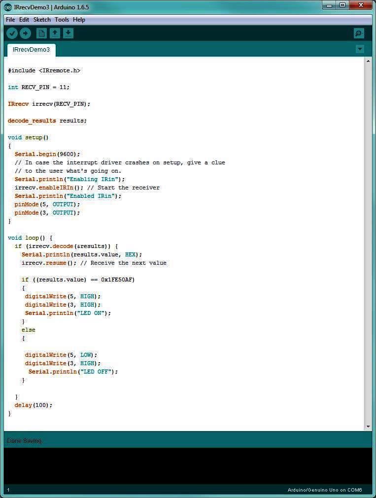
- I wrote the following code as shown below:
- Press "CTRL + SHIFT + U" to upload the code using the programmer
- I tested the functionality and tested as below.
RECORDING IR CODES FROM REMOTES:
-
HOW TO RECORD THE IR CODES THAT I WILL ADD TO MY ANDROID PROGRAM?
There are TWO ways to achieve that task:
- To get the remotes hexa-decimal IR codes from websites or manifacturer manuals.
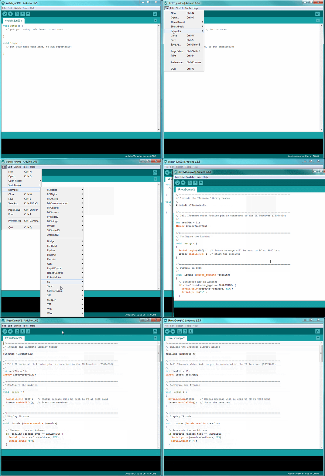
- To use IRRemote example code that record IR code and dump it to Serial Monitor with all the needed info, I used this method.
- Connect Arduino with the IR receiver as shown below:
- In Arduino IDE: Open File-> Examples -> IRremote ->
- I tested the functionality and tested as below.
PROGRAMMING ANDROID APPLICATION (APPLICATION INTERFACE):
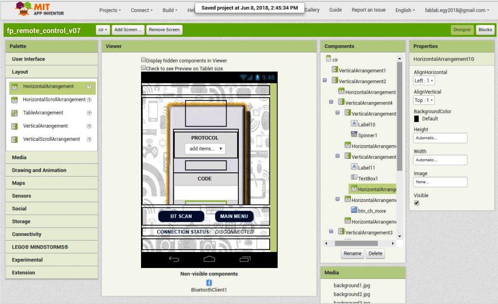
- The first step I performed is to sketch on paper the hierarchy of the application and the number of screens that I will have in the application and I decided to design it as below:.
- SCREEN 1: screen that represent application name and has an "ENTER" button to move to the main menu.
- MAIN MENU SCREEN: screen that displays a menu of buttons where each button direct to a device to be controlled with IR. (
- TV, SATELLITE AND LIGHT SCREENS: THREE screens with each of them has a graphical interface of a remote.
- I used MIT APP INVENTOR to develop my Android application interface, for more information about how to develop an interface using MIT APP INVENTOR you can check my WEEK 13 assignment.
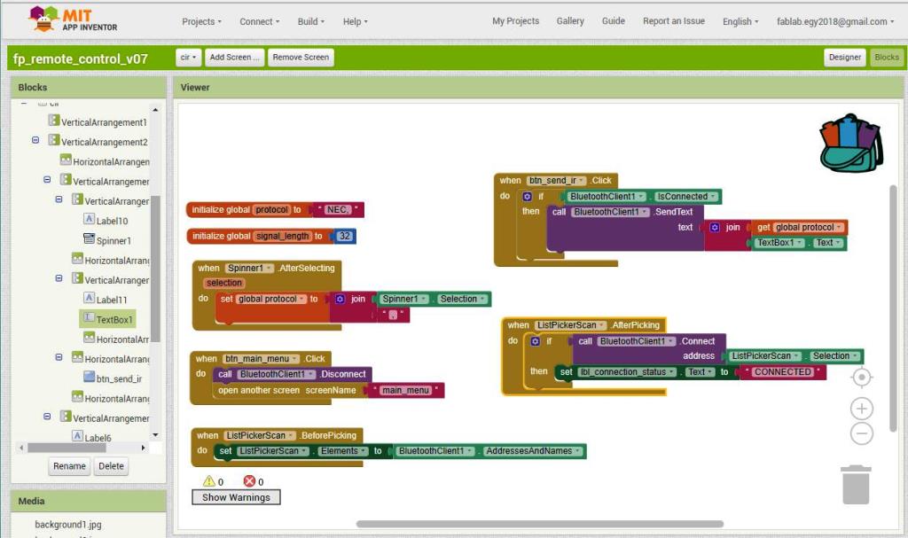
- For SCREEN 1: I designed the screen and I added the code blocks as shown below:
- For SCREEN 2 (Main Menu): I designed the screen and I added the code blocks as shown below:
- For SCREEN 3 (TV Remote): I designed the screen and I added the code blocks as shown below:
- For SCREEN 4 (Satellite Remote): I designed the screen and I added the code blocks as shown below:
- For SCREEN 5 (Light Remote): I designed the screen and I added the code blocks as shown below:
- In the last minute I decided as well to add a screen where a user can select a protocol and type the frequency, this screen should give the user the flexibility to try other devices and not to be restricted to the codes I hard coded in my program. so I created this screen by adding the foloowing blocks and design:
INTEGRATION AND ASSEMBLY:
TRANSMITTER UNIT ASSEMBLY (UNIT A):
- Now comes the most important stage - THE INTEGRATION - which is basically to integrate the outcomes from all the previous stages to ensure they all work together.
- For integrating and assembly of the transmitter unit I performed the following steps:
- I assembled the press-fit enclosure from the laser-cut plywood pieces.
- For the transmitter (UNIT A): I then placed the PCB board holders in the base of the enclosure and then I placed the PCB Circuit board on the top of it (It was fixed using double-tape).
- I passed a USB cable through the USB opening in the enclosure and used it to power up the Transmitting board. Then I closed the enclosure and powered it up.
RECEIVER UNIT ASSEMBLY (UNIT B):
- For integrating and assembly of the receiver unit I performed the following steps:
- I passed a male 220v AC power plug cable in the POWER IN slot in the enclosure and a female 220v AC Power plug in the POWER-OUT slot in the enclosure.
- I connected the power cables to the 220V AC - 5v DC module and the solid state relay as shown in the image below:
- Then I placed the connected board in the base of my enclosure on the top of the PCB holders.
- I placed the shelf on the top of the connected "solid-state relay" and the "220v AC - 5v DC" module.
- I then placed the receiver PCB board on the shelf.
- I connected the "IR Receiver component" to the "IR Receiving PCB Board" using a cable with sockets at both ends as shown in the image below, then I fixed it to the transparent side of the enclosure.
- I closed the enclosure and then I powered it up and tested it.
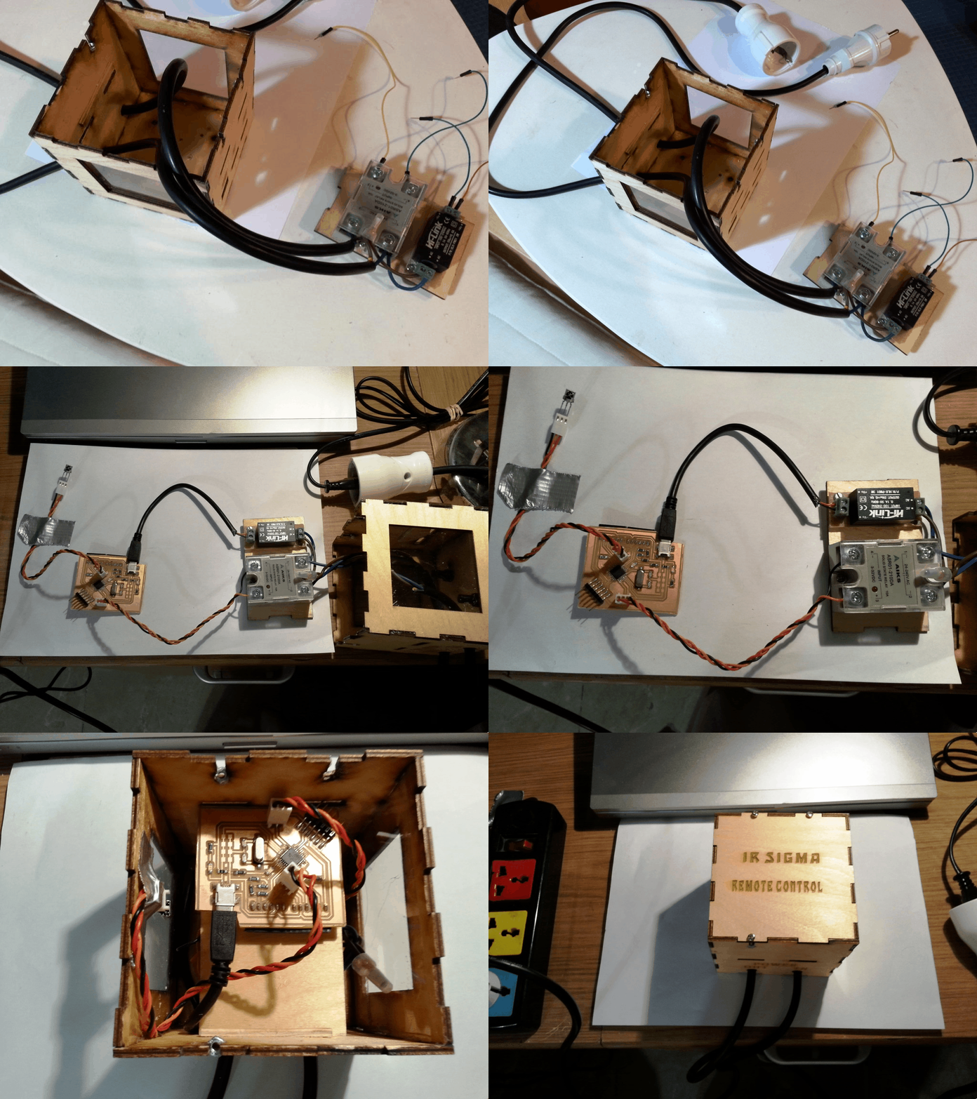
The main reason behind that is simply to ensure that the IR reveiver sensor will be as close as possible to the transparent layer in the enclosure side and accordingly incease the sensitivity of the overall device to any transmitted IR signal.
LICENSE:
- I decided to use Creative Commons licences and I chose Attribution-NonCommercial-ShareAlike 4.0 International (CC BY-NC-SA 4.0).
- The "Attribution-NonCommercial-ShareAlike 4.0 International (CC BY-NC-SA 4.0)" license allow others to remix, tweak, and build upon my work non-commercially, as long as they credit me and license their new creations under the same identical terms, more details can be found in THIS ASSIGNMENT
-

This work is licensed under a Creative Commons Attribution-NonCommercial-ShareAlike 4.0 International License.
ACKNOWLEDGEMENTS:
- At the end I would like to acknowledge and pass my full gratitude to:
- My local Instractors May El-Dardiry and Mohammad Abu-ElHaggag for their commitment to help and support.
- My global Instructors Ohad for pushing to extend my limits and Francisco for his efforts to review my documentations.
- And last but not least: All my colleagues and specially Khaled Youssef.
Files:
- ENCLOSURE: FUSION F3D FILE. | . EXPORTED DXF ZIP FILE. | . RD WORKS PROJECT RLD FILE.
- ACCESSORIES :
- BALL HINGE: FUSION F3D FILE. | . STL FILE.
- PCB HOLDER: FUSION F3D FILE. | . STL FILE. | . MAKERBOT PROJECT FILE.. | . X3G FILE
- PCB DESIGN AND PRODUCTION :
- TRANSMITTER / RECEIVER: SCHEMATIC.. | . BOARD. | . TRACES. | . OUTLINES. | .
- 220V AC / 5V DC: SCHEMATIC. | . BOARD FILE.. | . TRACES. | . OUTLINES.
- IR TRANSMITTER BREAK-OUT PCB: SCHEMATIC. | . BOARD. | . TRACES. | . OUTLINES.
- IR RECEIVER BREAK-OUT PCB: SCHEMATIC. | . BOARD. | . TRACES .. | . OUTLINES.
- EMBEDDED PROGRAM : IRREMOTE LIBRARY.. | . IR TRANSMITTER INO FILE.. | . IR RECEIVER INO FILE.
- ANDROID APPLICATION INTERFACE : ANDROID APPLICATION AIA FILE.
- PRESENTATION : SLIDE. | . MP4.
- DATASHEET : ATMEGA 328-PU. | . HLK-PM01 DATASHEET.
