Assignment 6
Electronics Design

How to:
This week is all about electronics designs, that means getting to know the whole process from designing a schematic and a board, milling the PCB and soldering. In the week's group assignment we tested the test equipment in your lab to observe the operation of a microcontroller circuit board. Detailed information about this can be read on the Group project page.
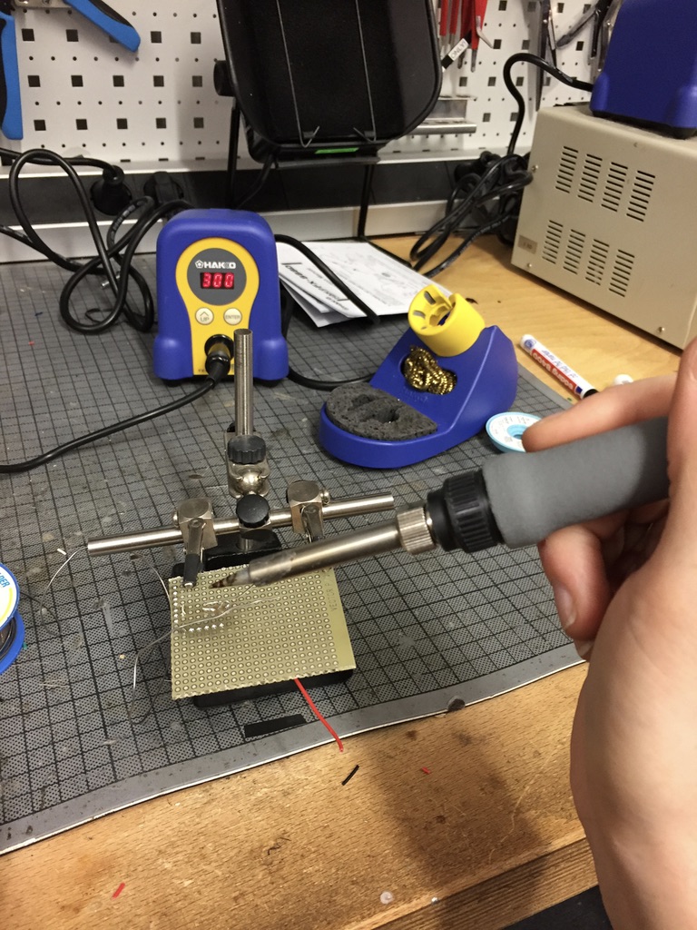
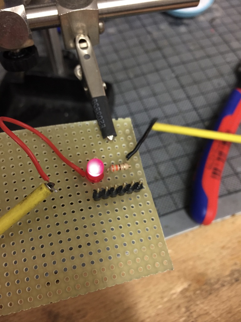
Except soldering, this field is totally new for me. Therefore, first of all I looked for tutorials that would help me gaining knowledge. Furthermore, our local instructor gave us an introduction into basic electronic topics, designing with Eagle and soldering. In this tutorial we soldered basic elements like an LED and pin headers.
General steps:
1. Design schematic and board files in EAGLE.
2. Use CAM processor in eagle to produce BOT, .DRD, .TOP, .BOA files.
3. Prepare for milling with CircuitCAM.
4. Using the PCB milling Program BoardMaster.
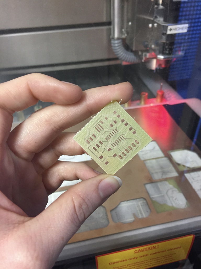
5. Milling itself.
6. Prepare for soldering and assembling.
7. Assemble and solder components to PCB.
Schematic and Board Design
1. First of all I installed the Eagle software on my laptop. To get to know how to use the software I had a look into the following tutorial: Eagle tutorial.
2. Our exercise for this week was designing the Hello-World-Board. The link shows the board which and I used it as a template for the design. Additionally, we were asked to
add at least one button and one LED (including a current-limiting resistor) into our board design.
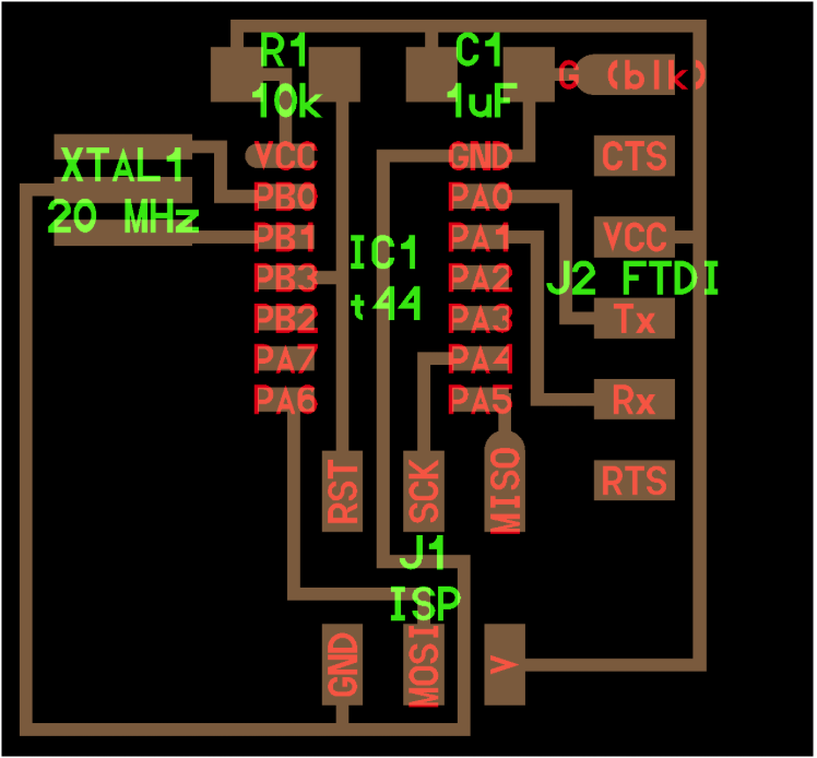
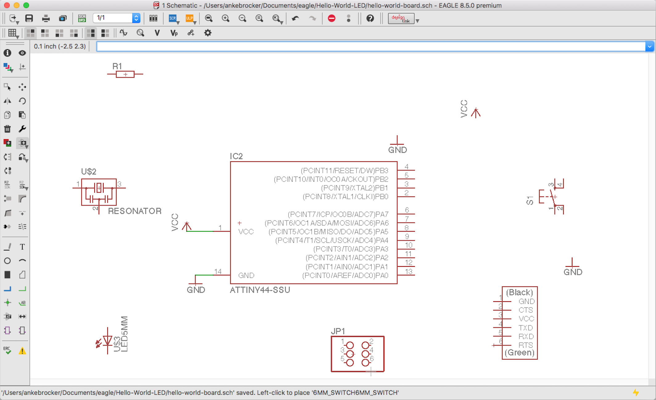
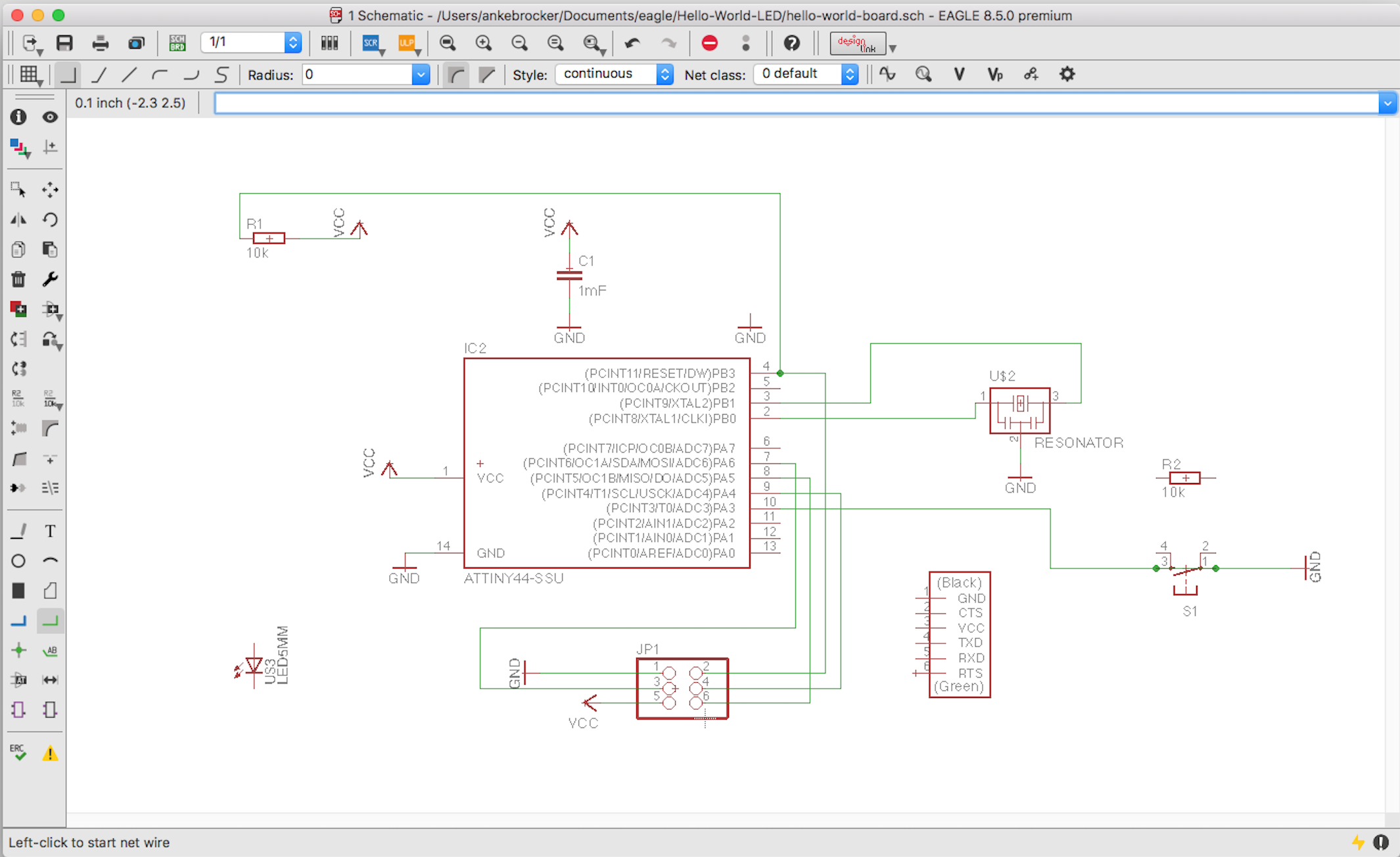
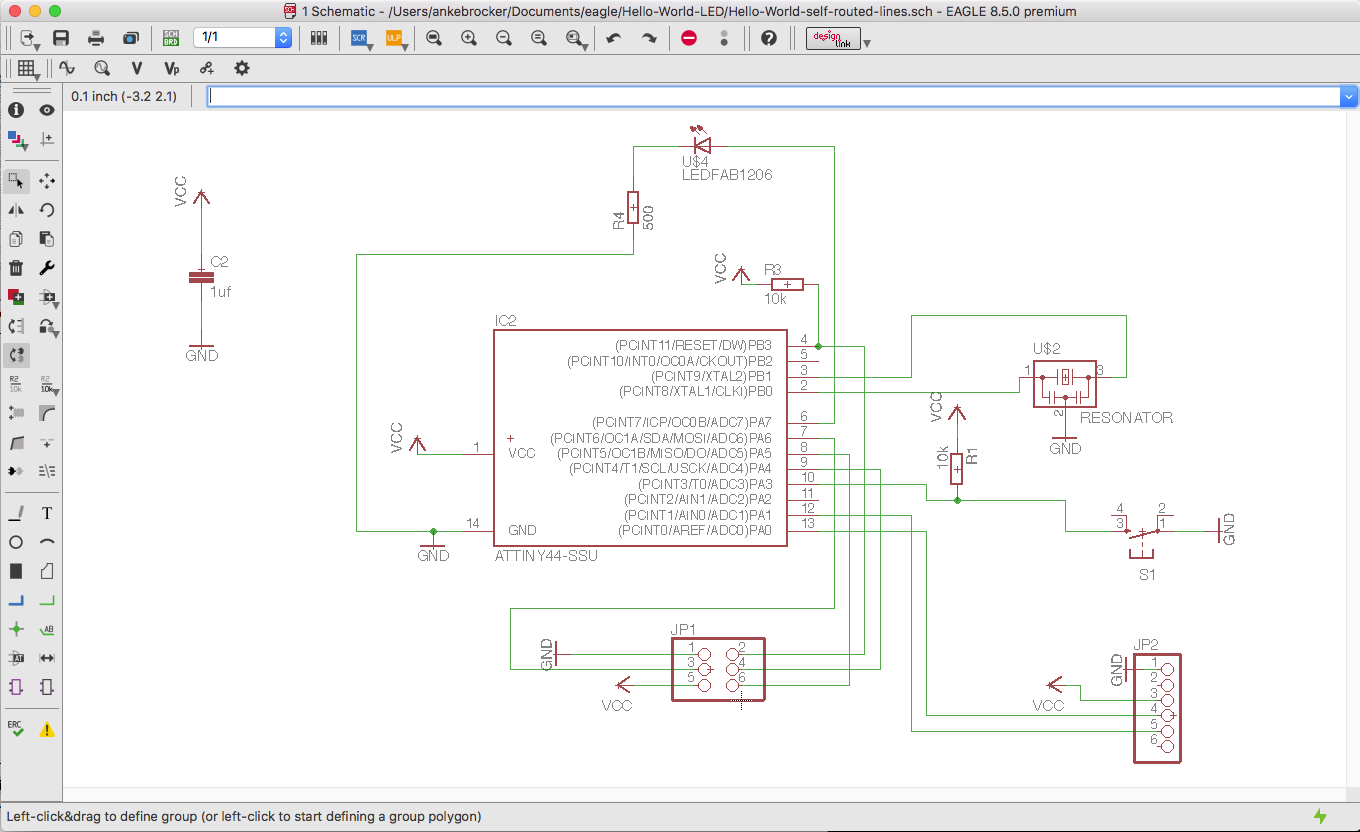
4. After designing the schematic I started designing the board of my schematic. To start I pressed
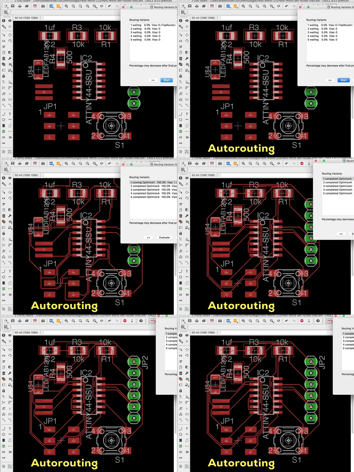
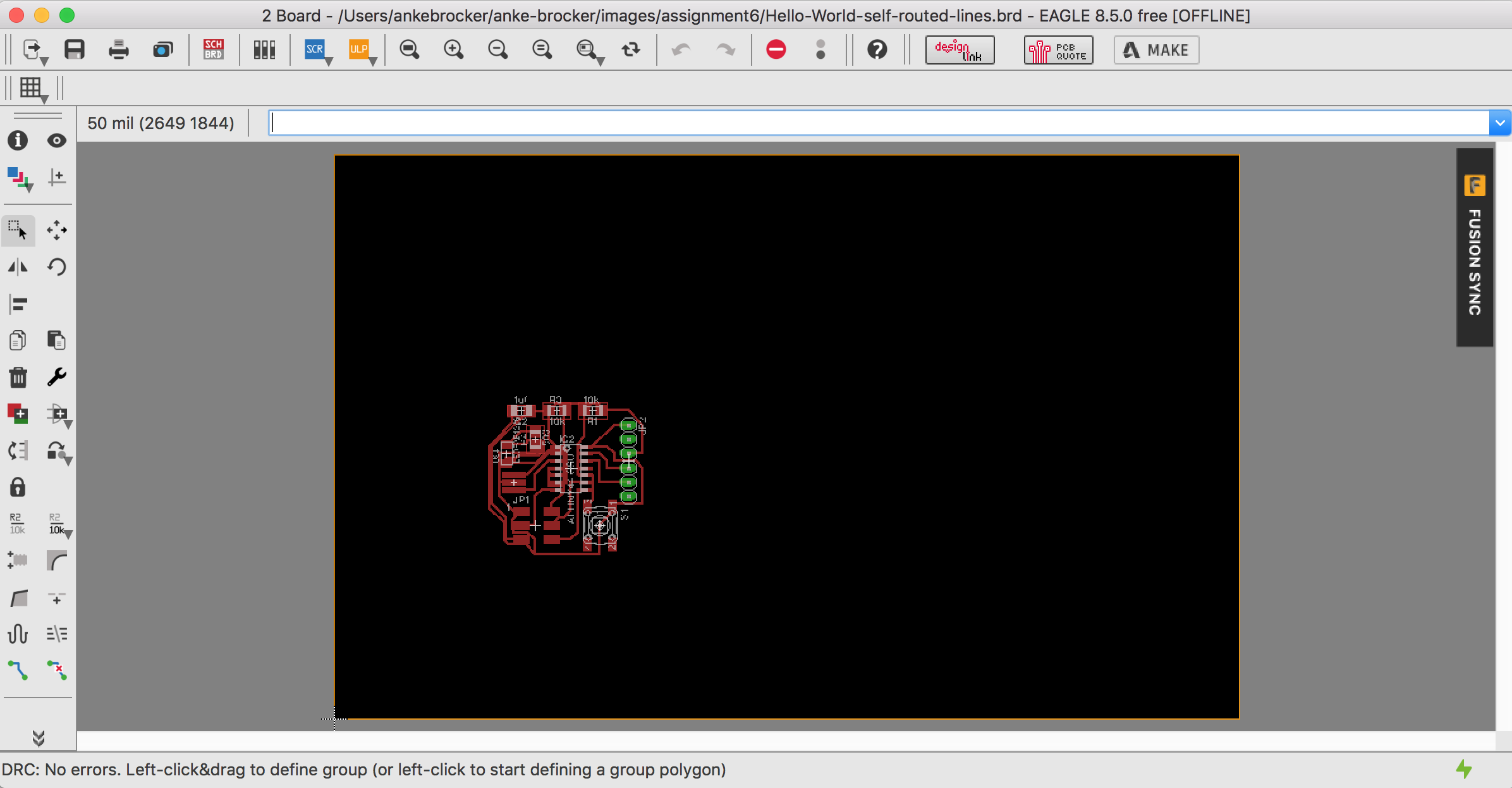
Eagle provides an autoroute option. I tested this several times until autorouting was able to route everything without producing overlaps. Even if the autorouting did produce a working board, I decided to manually route the connections between the components as a human being is most times able to be more clever than the autoroute tool. Additionally, I wanted the routes to have a bigger width than with the autoroute tool. Still, I used the autoroute result as inspiration during my manual routing to assure I do not create overlaps.
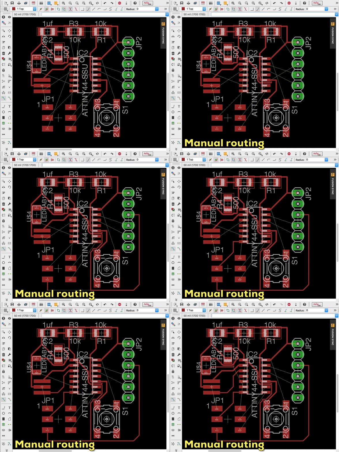
5. All in all, it took about an hour to route all connections manually. In the beginning it was hard to route properly as meeting the correct start and end point of a route needs some training. You can find the schematic and board files at the end of the page.
ERC and DRC Check
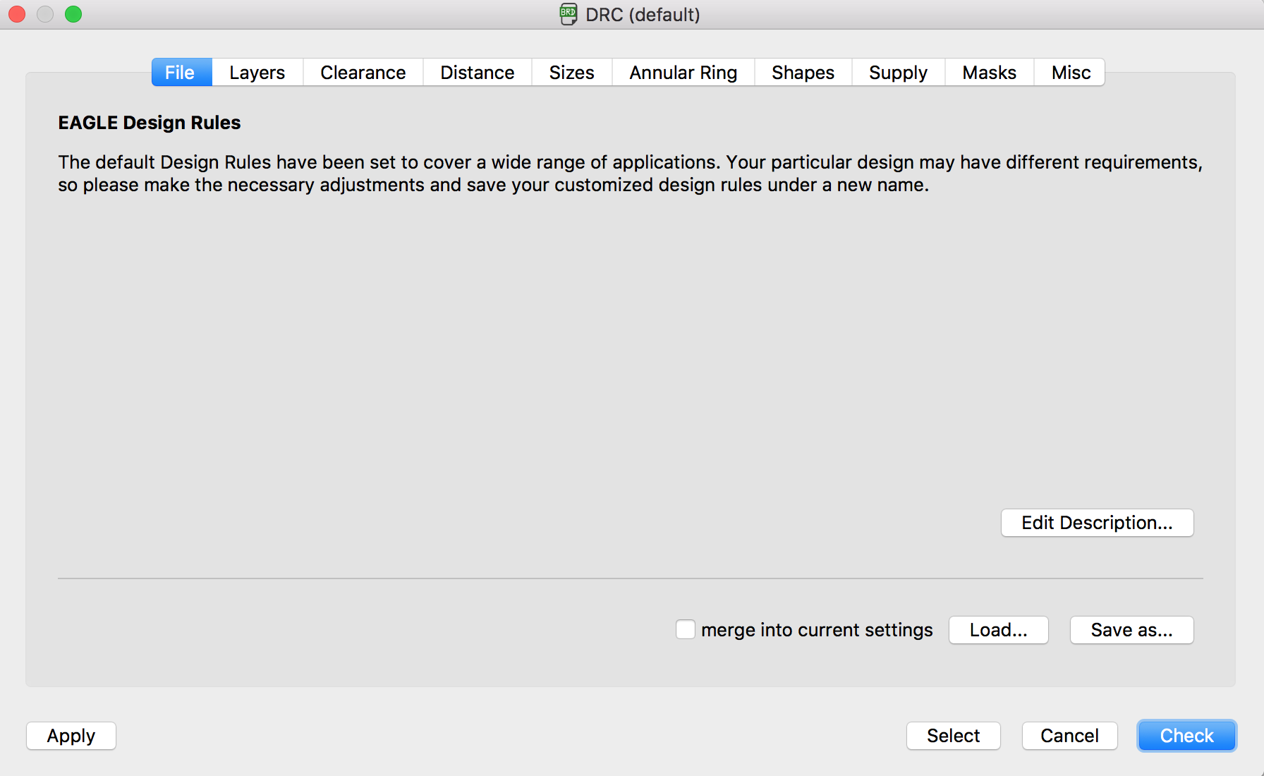
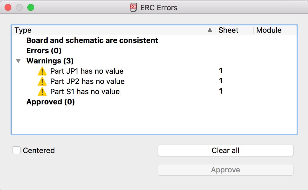
Eagle provides two tools that help you to check whether your board is correct or not: a.) electrical rule check (ERC) and b.) design rule check (DRC).
a.) The ERC checks e.g. for any open or overlapping pins and ports on your schematic and will give out these errors.
b.) The DRC establishes a set of boundaries for trace widths, component spacing, via diameters that you can check for your board.

Cam Processor Eagle
The steps in the Cam processor of Eagle are the same as in the FabISP week. Have
a look there to see the steps you need to follow.
This time also the .DRD file was prodcued as the mill had do drill holes in the board for my pin headers.
CircuitCAM Software
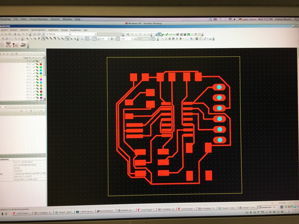
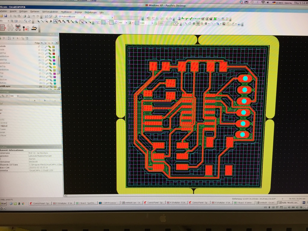
Before the board can be milled it needs to be transferred into a LMF file which can be opened by the boardmaster software used by the milling machine. These steps again follow the same procedure as in the FabISP week. The two pictures underneath show the board during the CircuitCAM software process.
Board Master Software & Milling
In our FabLab we have a LPFK milling machine. With the software boardmaster you can control the milling machine. Important advices when mill your PCB are mentioned in the FabISP week. Please follow these advices.Following you see the steps to prepare the LMD file in boardmaster to mill it: These steps are very similar to the FabISP week. Still I will describe them in detail again as I include different screenshots belonging to the 'Hello-World-Board'.
1. When clicking the symbol to export an LMD file in CircuitCAM the file was sent directly to the boardmaster software.
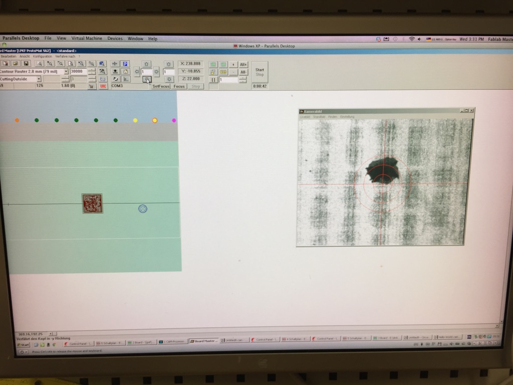
2. Now you need to move the milling head into the correct position. As a hint, mark your PCB in the mill with a dot where you want to mill your PCB. Look for this dot with the camera of the mill machine head by moving it with these
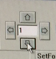 arrows in the boardmaster. You can define the step size with the number in the middle of the arrows.
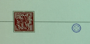
3. Now move the mill head to the camera head by clicking 'Verfahre nach < Kopf>>Kamera'. Afterwards, also move the digital board with the tool ![]() in the boardmaster software to the blue circle, which indicates the mill head
in the boardmaster software to the blue circle, which indicates the mill head
 .
.
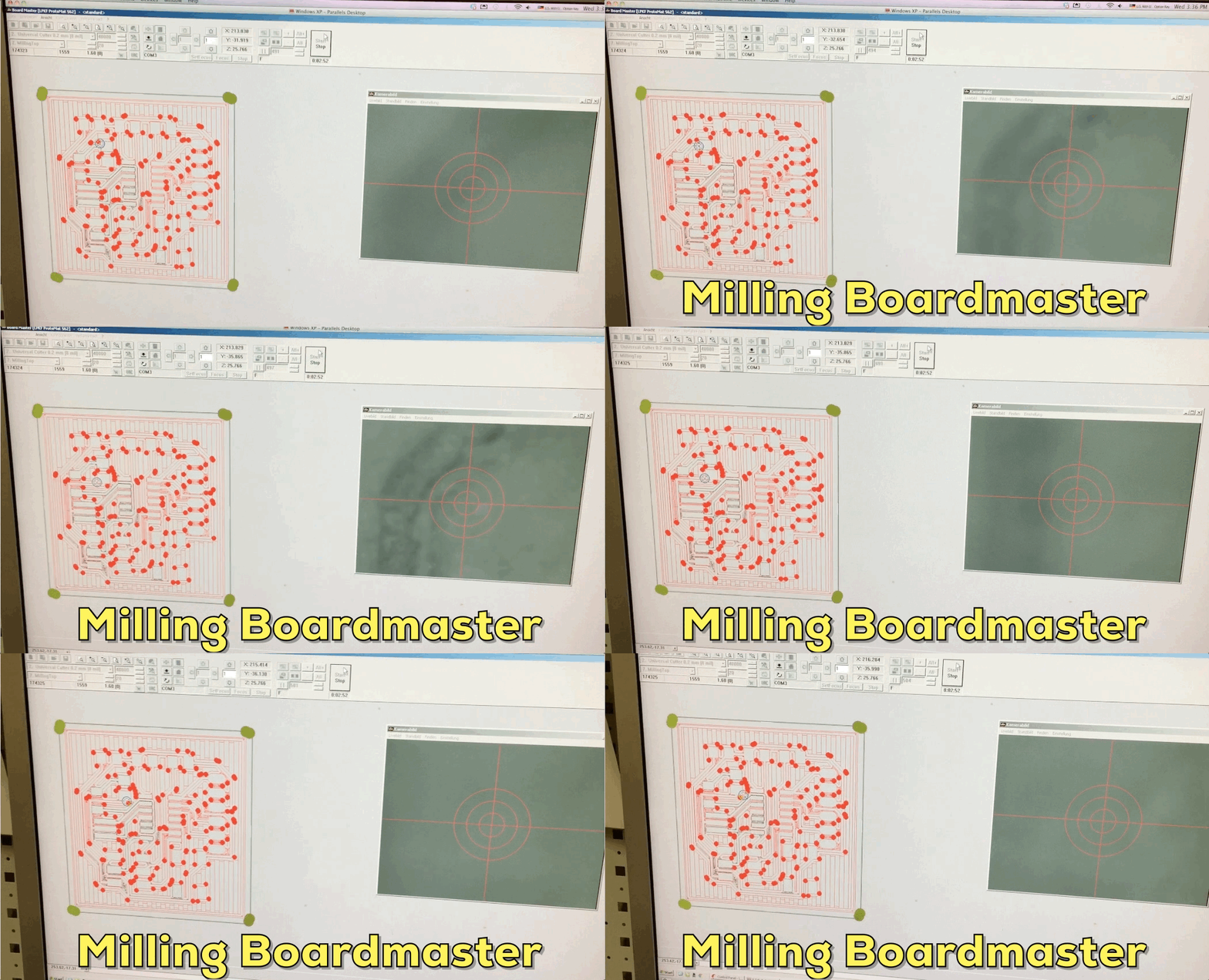
4. You need to execute three parts to complete your PCB: Drilling plate, Milling Top, Cutting Outside. Those need to be executed separate and after each other. You can choose the parts here
![]() .
.
5. Every time before you start milling one part you need to click 'All+' and then 'Start'  . Follow this instruction for each part and mill your PCB.
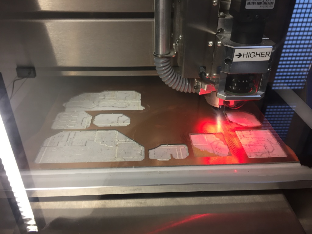
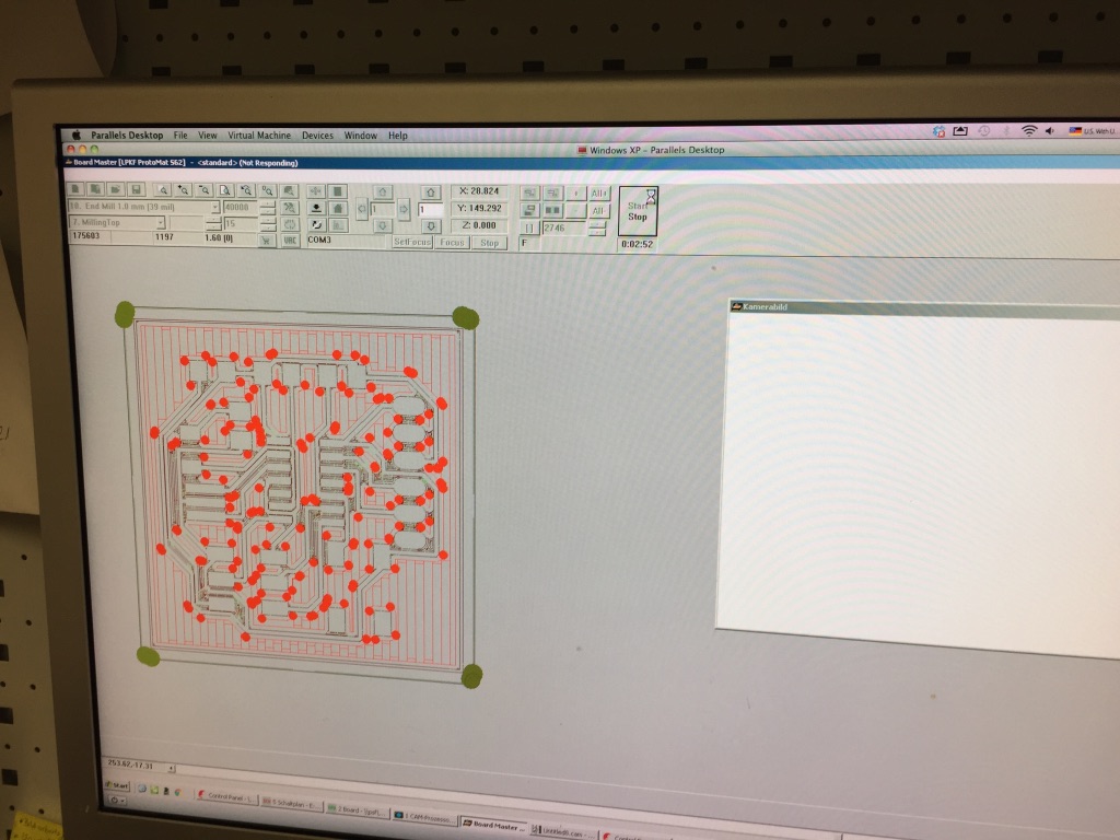
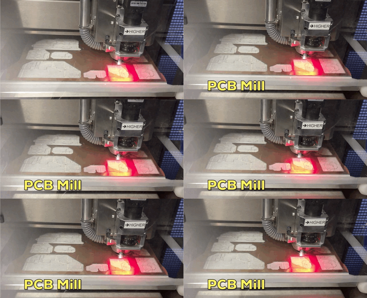
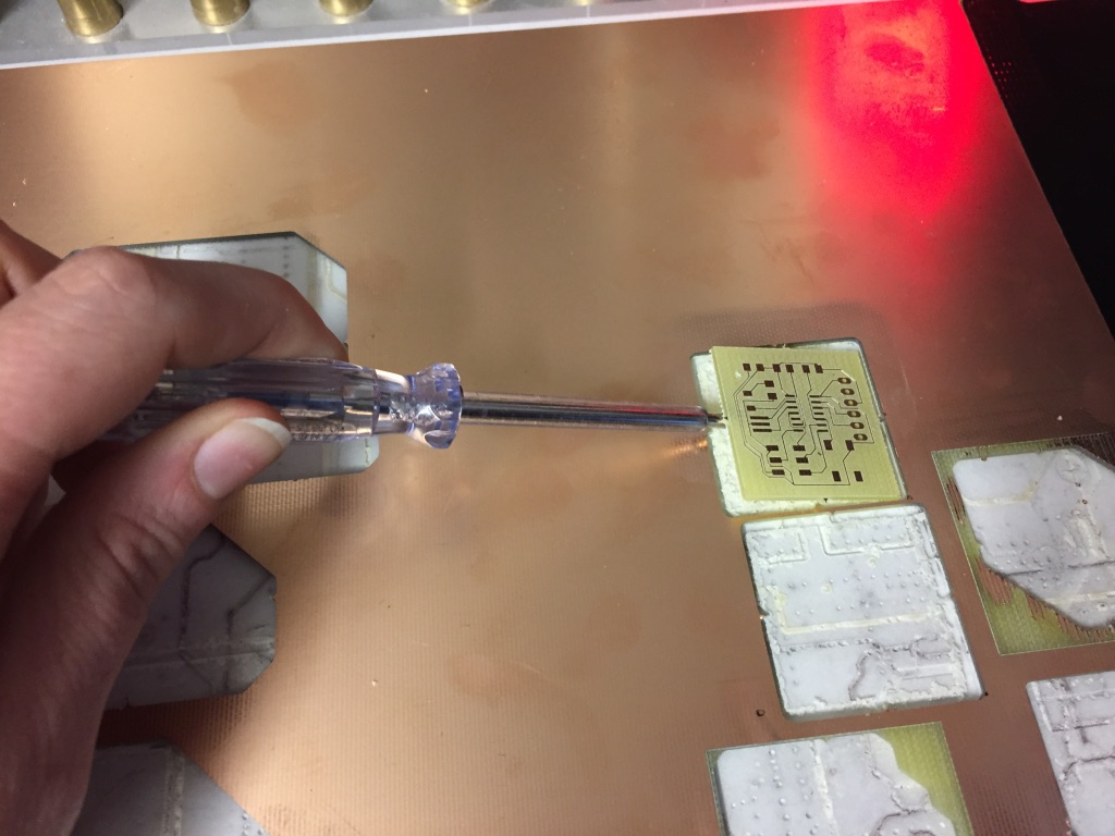
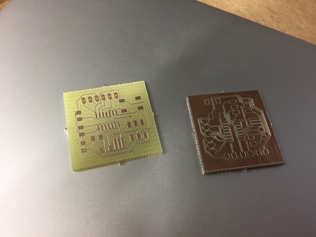
6. After executing all milling dissolve your PCB from the shield.
Soldering
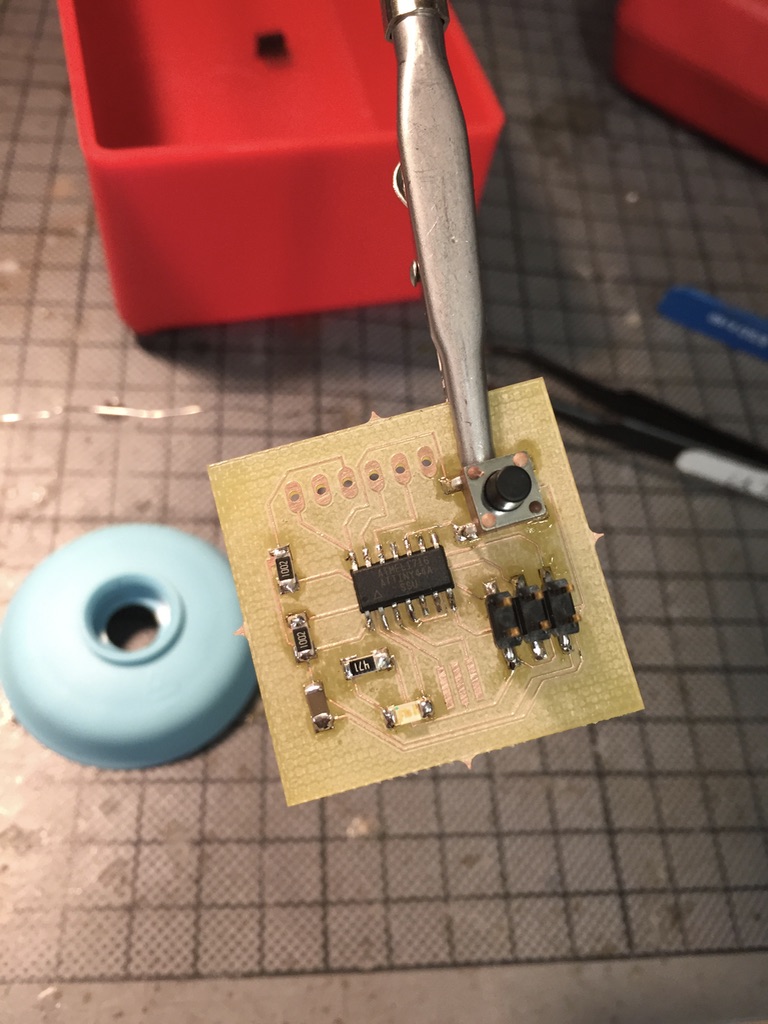
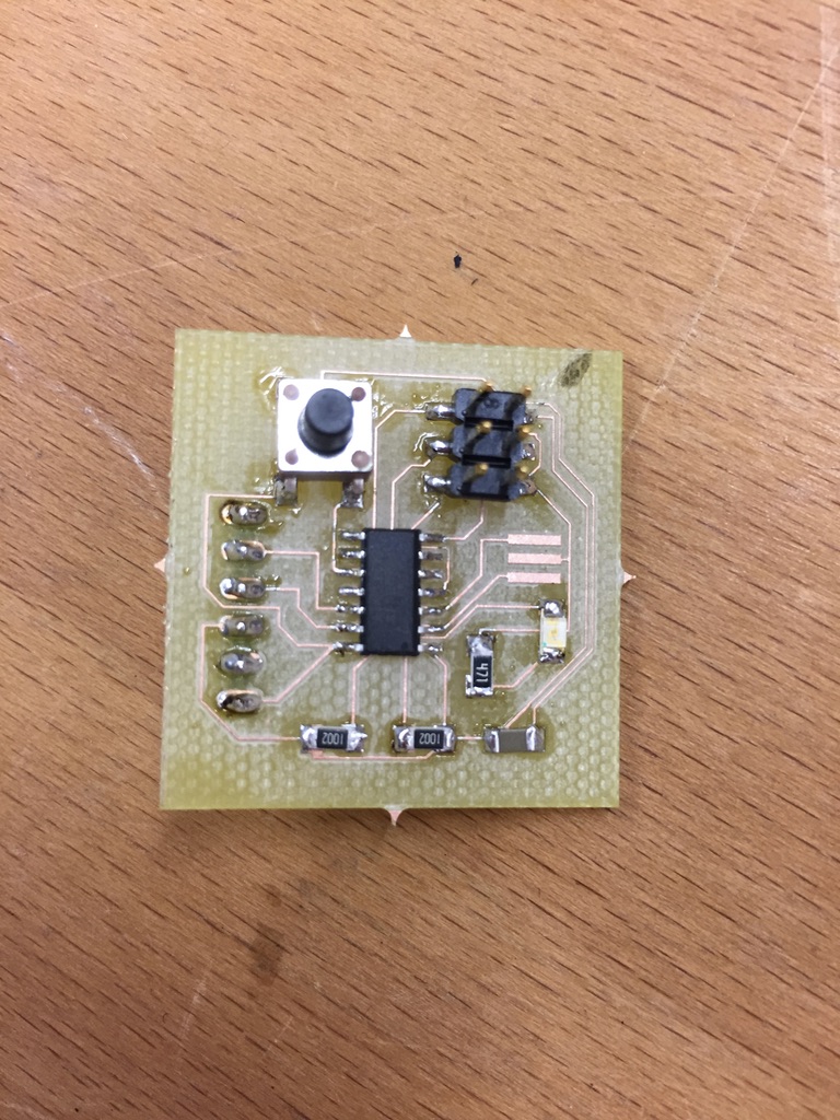
As mentioned before soldering was the only part of electronic design I had experience in. First, I collected all the needed components from the FabLab drawers:
1 x Attiny 44
1 x 10mF SMD Capacitor
2 x 10kΩ SMD Resistor
1 x 470Ω SMD Resistor
1 x blue SMD LED
2 x 3 SMD Pinheader
1 x 6 THT Pinheader
1 x SMD button
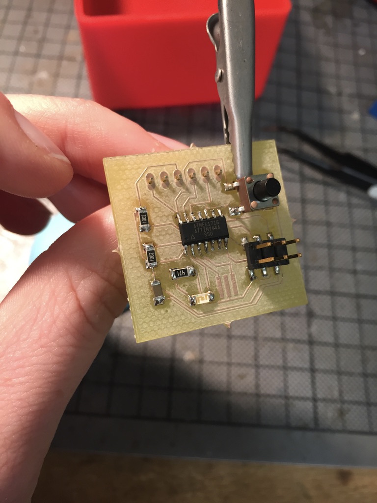
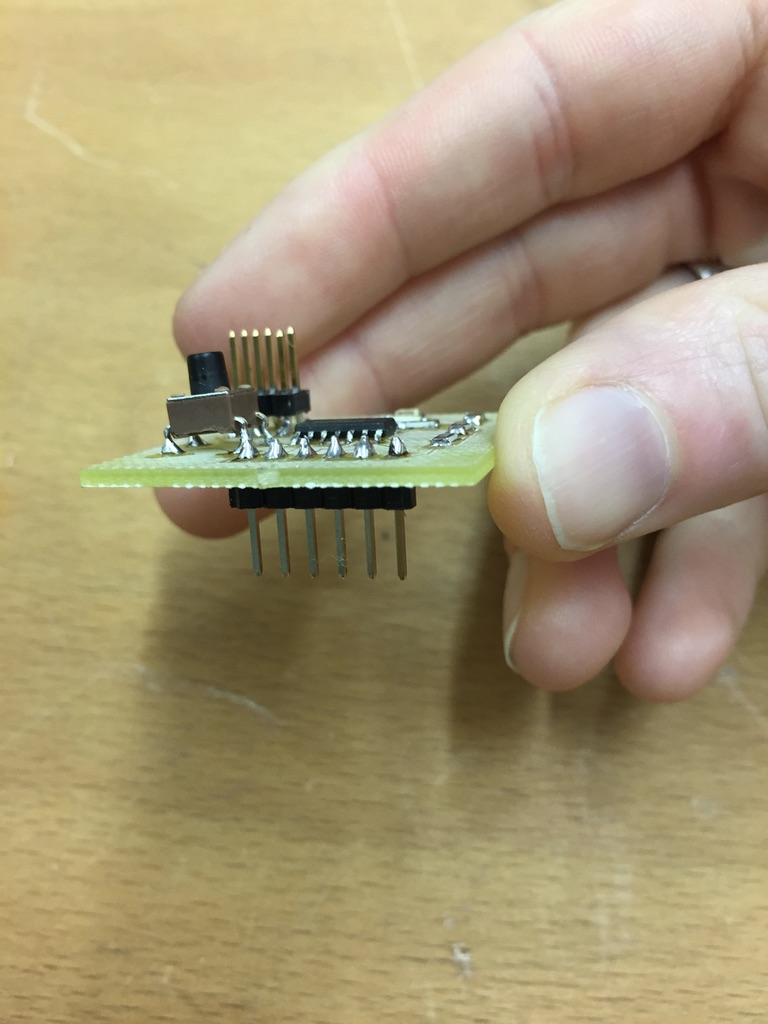
Then I started soldering. At first, I soldered the ATTiny and afterwards all the other SMD parts to have an even surface to solder on. At last I soldered the 1 x 6 pinheader, which is a THT.
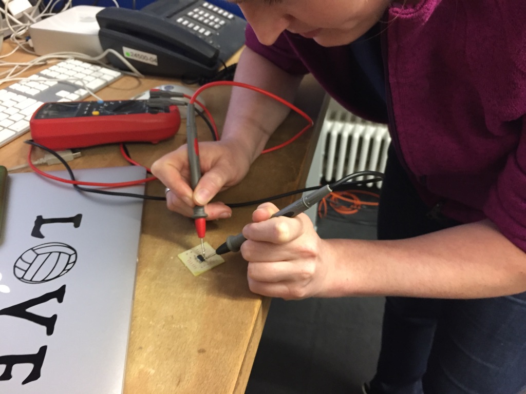
During soldering I used a multimeter to assure regularly that I did not solder 'short cuts'.
I added a 20MHz oscillator to my board and schematic design but did not populate the 20MHz oscillator. The reason is that for the purpose of this board (i.e. programming a push button
and a LED) the internal clock of the microcontroller is sufficient.
