Week 06 – Embedded Programming
Group Assignment – I2C Signal Analysis Using Oscilloscope
1. Oscilloscope Description
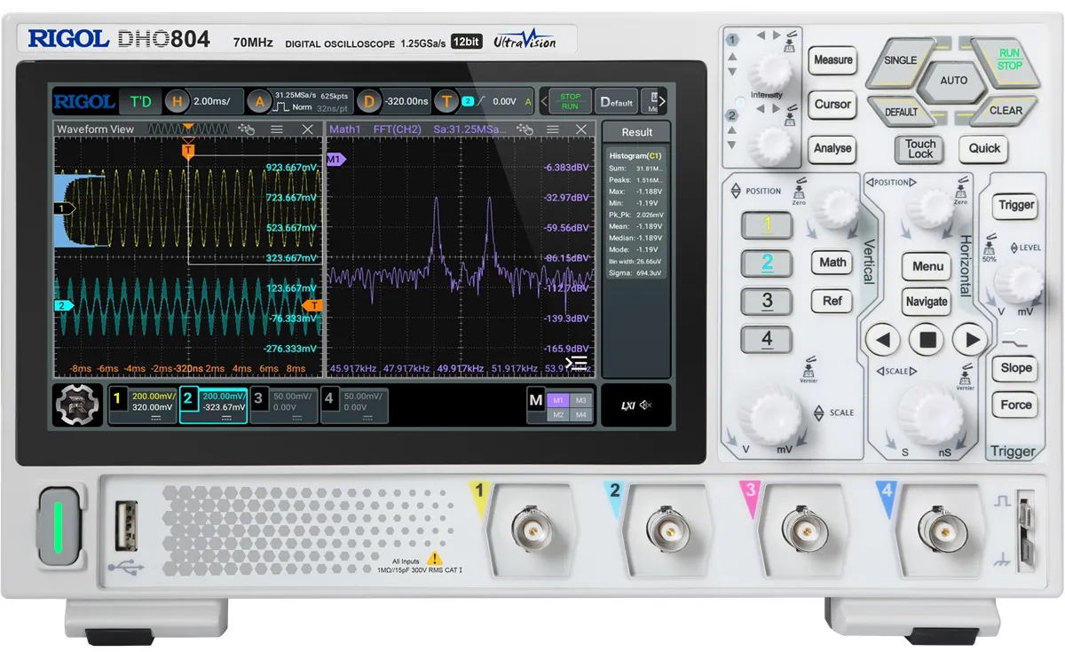
For this assignment, I used the Rigol DHO804 Digital Oscilloscope (70 MHz).
Main Specifications:
- Bandwidth: 70 MHz
- 4 Analog Channels
- Sample rate: up to 1.25 GSa/s
- 12-bit vertical resolution
- UltraVision architecture
- Automatic frequency and voltage measurements.
The oscilloscope was used to analyze I2C communication between the ESP8266 and the bus lines SCL and SDA.
2. Test Setup
- Microcontroller: ESP8266
- Protocol: I2C
- Logic level: 3.3V
- Channel 1 (Yellow) → SCL
- Channel 2 (Blue) → SDA
- Common ground between ESP8266 and oscilloscope.
Important:
I performed two different tests:
- I2C communication without external pull-up resistors
- I2C communication with pull-up resistors added
3. Test 1 – Without Pull-Up Resistors
I first tested the I2C bus without external pull-up resistors.
I2C uses open-drain (open-collector) outputs, meaning:
- Devices can only pull the line LOW
- The line needs a pull-up resistor to go HIGH
Waveform Without Pull-Ups
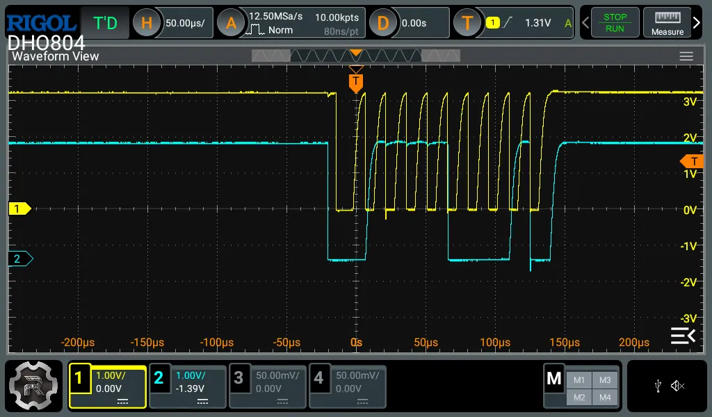
Observations:
- Rising edges were slower
- HIGH level was not perfectly stable
- Signal shape was not ideal
- Possible noise and weak logic HIGH
This happens because: - Without pull-up resistors, the line cannot properly return to 3.3V
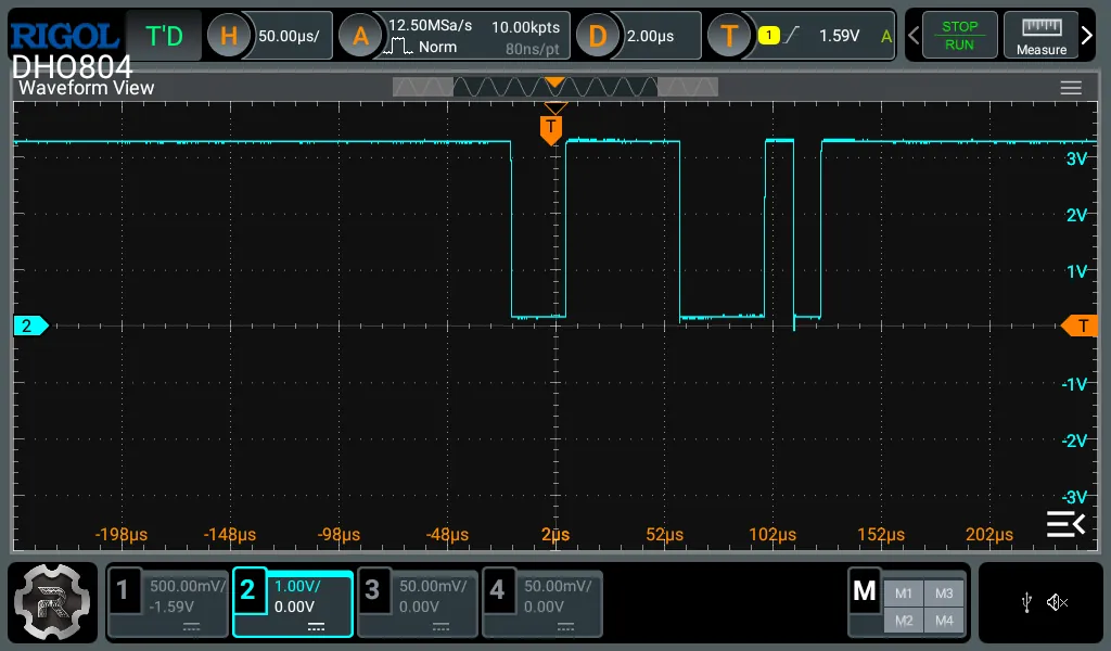
4. Test 2 – With Pull-Up Resistors
After that, I added external pull-up resistors on:
- SDA → 3.3V
- SCL → 3.3V
(typically 4.7kΩ or 10kΩ resistors)
Waveform With Pull-Ups
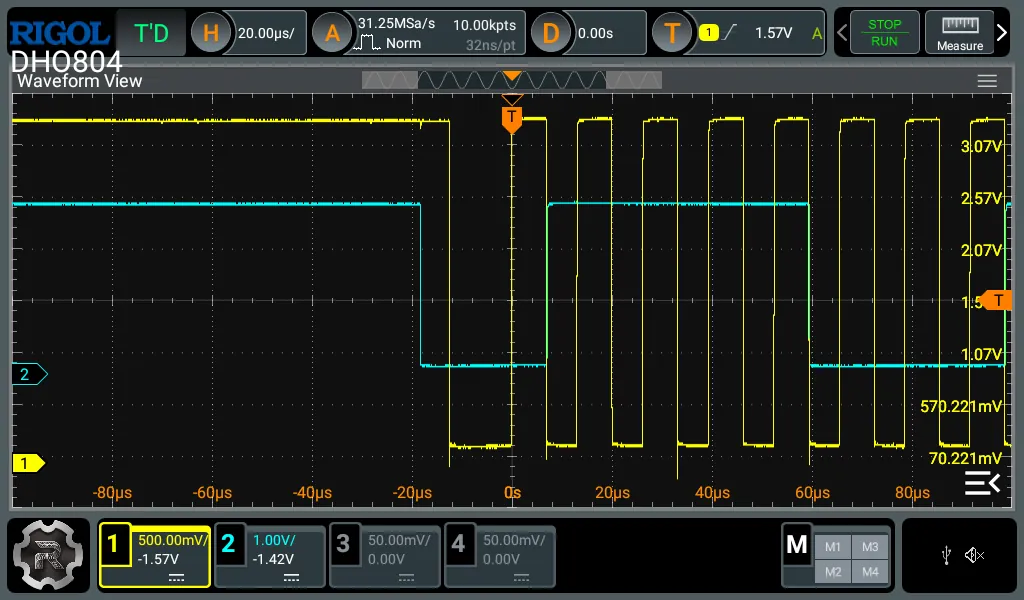
Observations:
- Clean rising edges
- Stable 3.3V HIGH level
- Sharp transitions
- Much cleaner digital signal
Measured voltage levels:
- HIGH ≈ 3.07V – 3.08V
- LOW ≈ 70mV – 80mV
This confirms proper 3.3V logic behavior.
5. I2C Signal Analysis
5.1 Clock Signal (SCL)
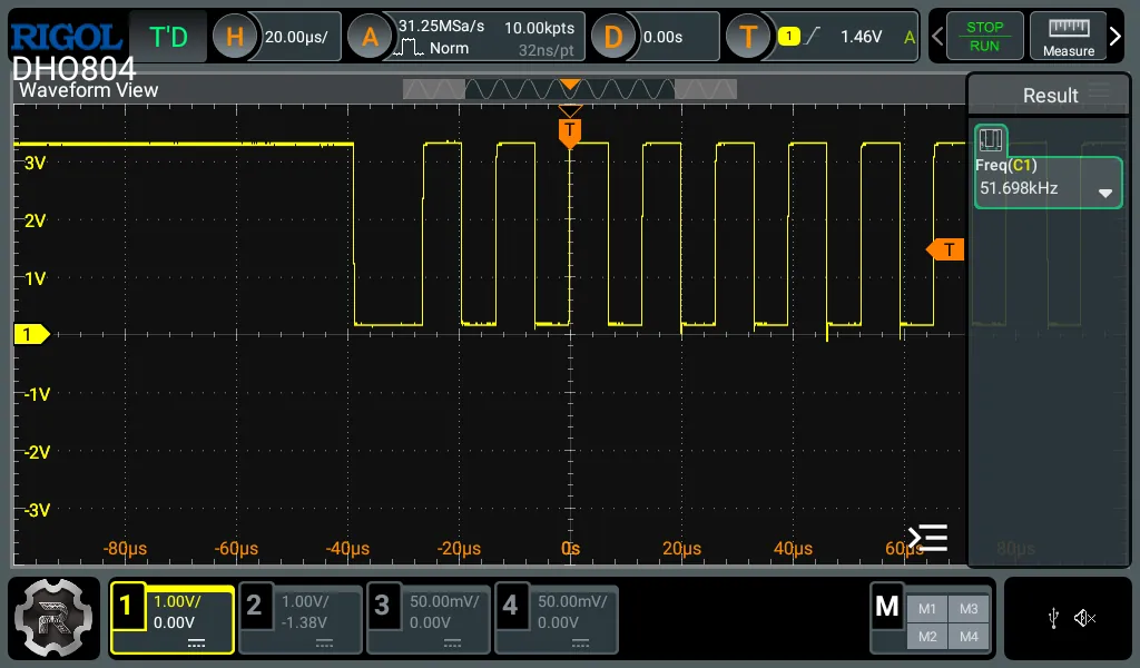
Measured frequency:
- ~47.6 kHz
- ~51.7 kHz
Average clock speed:
≈ 50 kHz
5.2 Data Line (SDA)
Observations:
- SDA changes only when SCL is LOW
- SDA remains stable while SCL is HIGH
This confirms correct I2C protocol timing.
Each clock pulse corresponds to one data bit.
6. Physical Setup
Full Test Environment
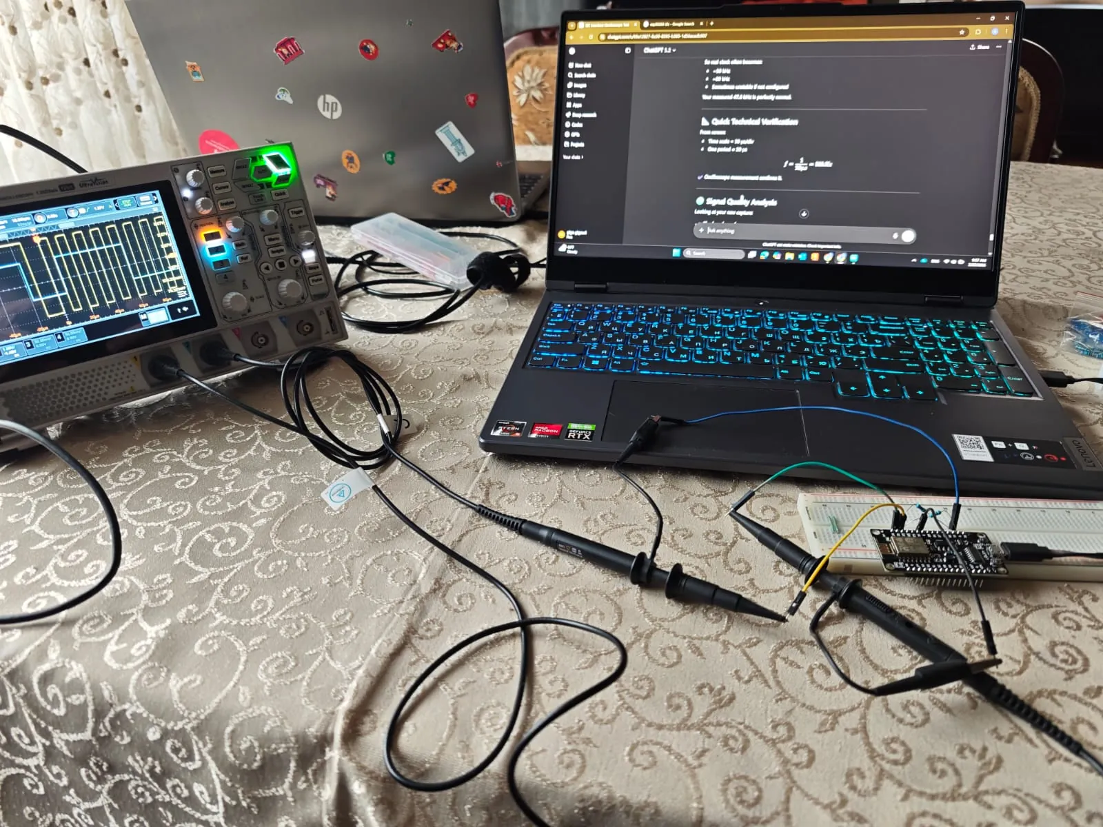
- Rigol DHO804 oscilloscope
- ESP8266 development board
- Breadboard wiring
- Probes connected to SCL and SDA
- Laptop for programming
Oscilloscope Display
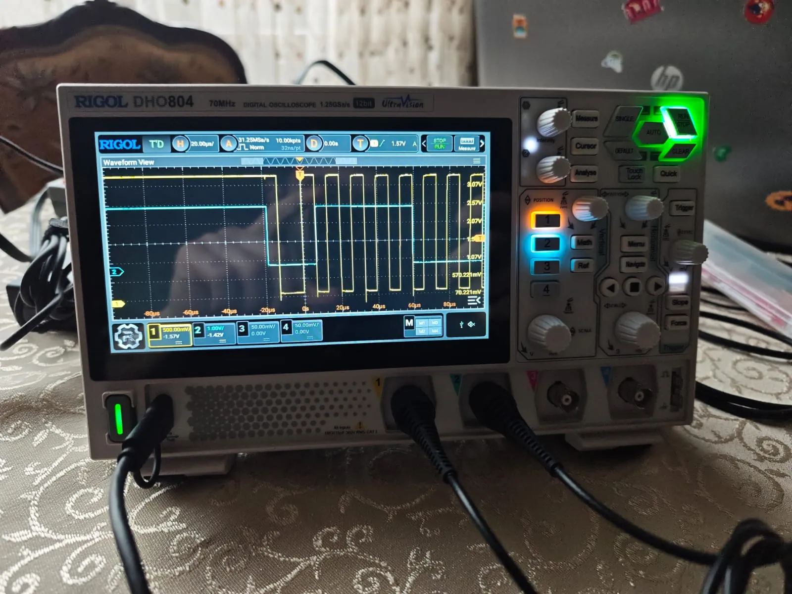
The display shows:
- Yellow: SCL
- Blue: SDA
- Microsecond time base
Week 06 — Electronics Design (Individual Assignment)
Software Used
For this assignment, I used KiCad for schematic and PCB design.
I chose KiCad because:
- It has a simpler and more intuitive interface.
- Library management is easier for small and medium projects.
- It is open-source and well suited for academic use.
- It integrates schematic, PCB, 3D viewer and Gerber export in one environment.
Design Rules Reference (PCB)
For general PCB layout rules and best practices, I used the following reference:
David L. Jones
PCB Design Tutorial
Revision A — June 29, 2004
📎 PCB Design Tutorial — David L. Jones (PDF)
Key Design Principles Applied
From this document, I followed these simple rules:
- Finish and verify schematic before starting PCB layout.
- Use grid and snap for clean placement and routing.
- Prefer 45° trace routing.
- Keep traces short and direct.
- Avoid unnecessary vias.
- Run ERC and DRC before fabrication.
- Use ground plane for better stability.
Schematic Design
For this assignment, I designed a simple development board based on:
STM32F030K6T6
The goal was to create a minimal but functional STM32 dev board that includes:
- 3.3V power regulation
- Decoupling capacitors
- NRST reset circuit
- SWD programming header
- Basic IO breakout
- Power input (USB / external input if applicable)
Full Schematic Overview
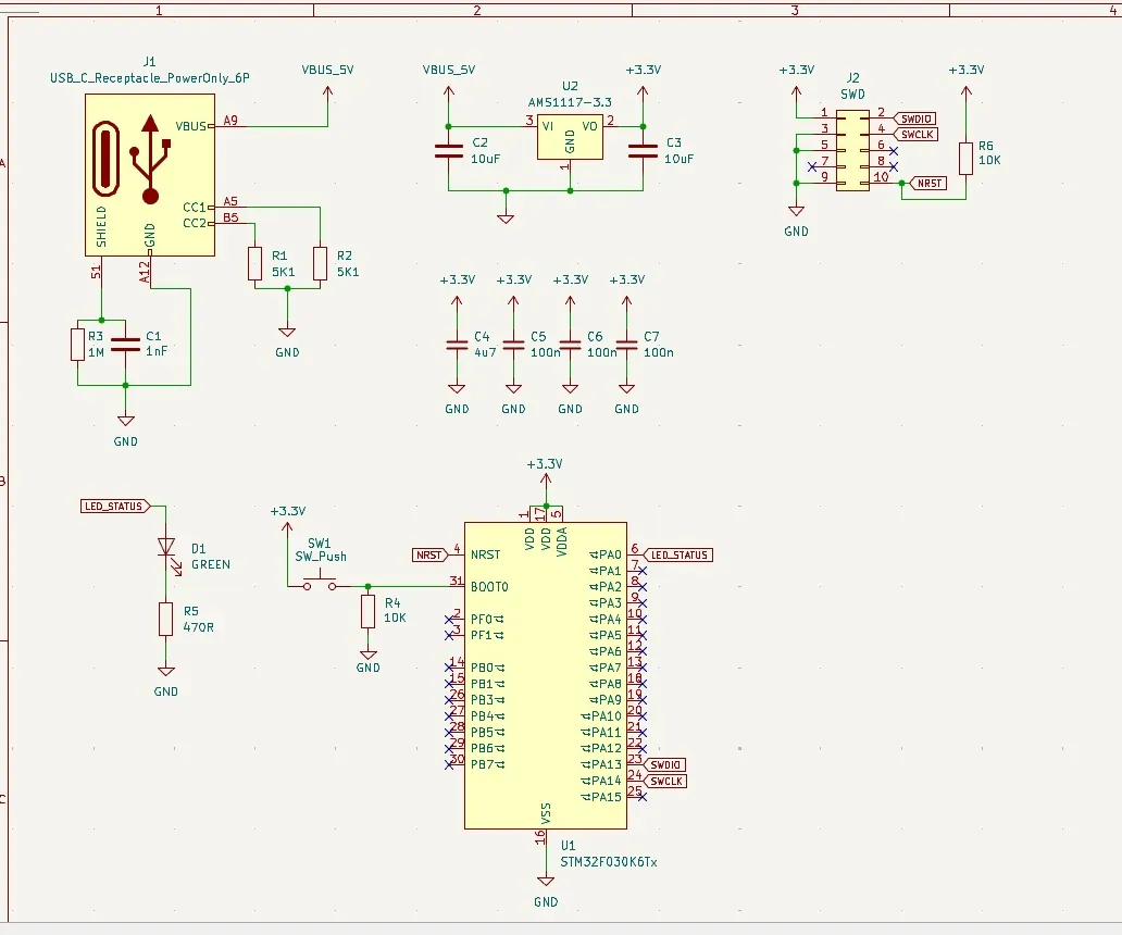
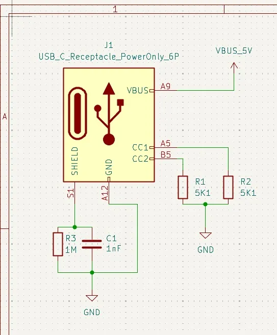
1️⃣ USB-C Power Input
The board is powered using a USB-C receptacle (Power Only configuration).
Design details:
- VBUS provides 5V
- CC1 and CC2 use 5.1kΩ resistors to GND (R1, R2) to indicate sink device
- Shield connected through RC network (R3 1MΩ + C1 1nF) to GND
- VBUS labeled as
VBUS_5V
This provides safe and standard USB-C 5V power input.
USB-C Section
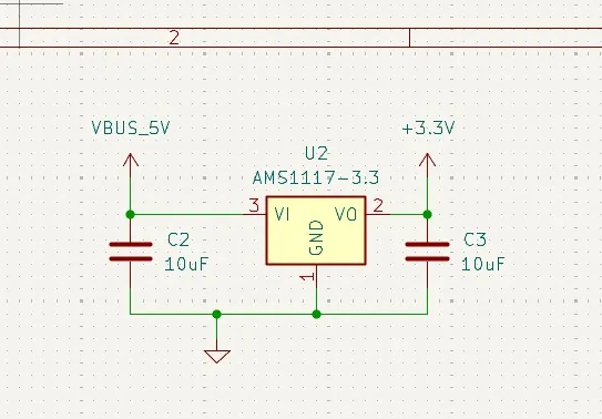
2️⃣ Voltage Regulation (5V → 3.3V)
The regulator used is:
AMS1117-3.3
Configuration:
- Input: VBUS_5V
- Output: +3.3V
- C2: 10µF input capacitor
- C3: 10µF output capacitor
This generates stable 3.3V for the STM32 and peripherals.
Regulator Section
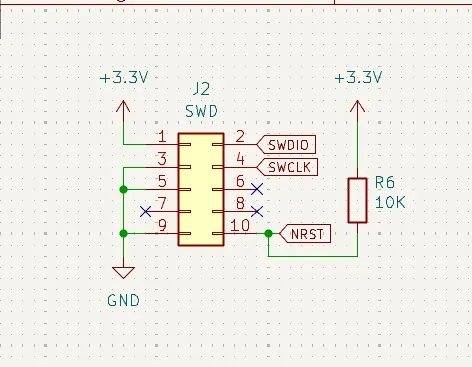
6️⃣ SWD Programming Header
A 10-pin SWD header (J2) is used.
Connected signals:
- SWDIO
- SWCLK
- NRST
- +3.3V
- GND
This allows programming with ST-Link or compatible debugger.
SWD Section
7️⃣ Status LED
A simple LED circuit was added:
- D1 (Green LED)
- R5 (470Ω current limiting resistor)
Connected to MCU pin (LED_STATUS).
Used for:
- Status indication
- Debug output
- Simple firmware testing