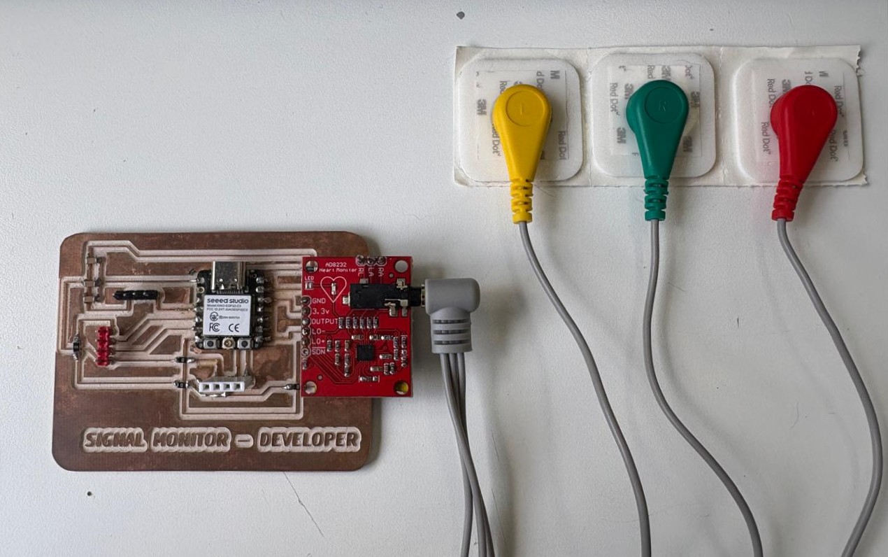
Input Devices
With the PCB design completed, I generated the fabrication files and prepared them in MODS for milling. The goal was to create the traces and the board outline using the milling machine.
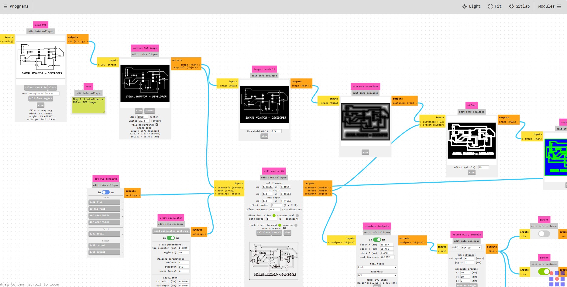
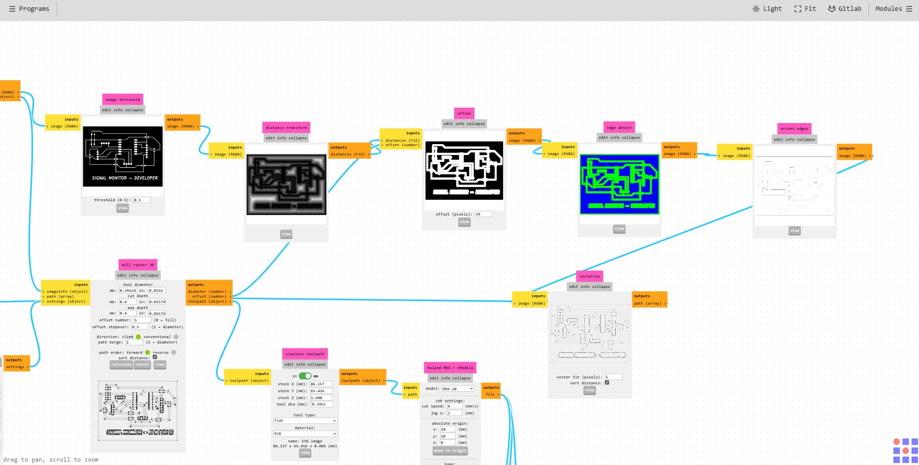
After checking the toolpaths, the file was ready to be sent to the milling machine.
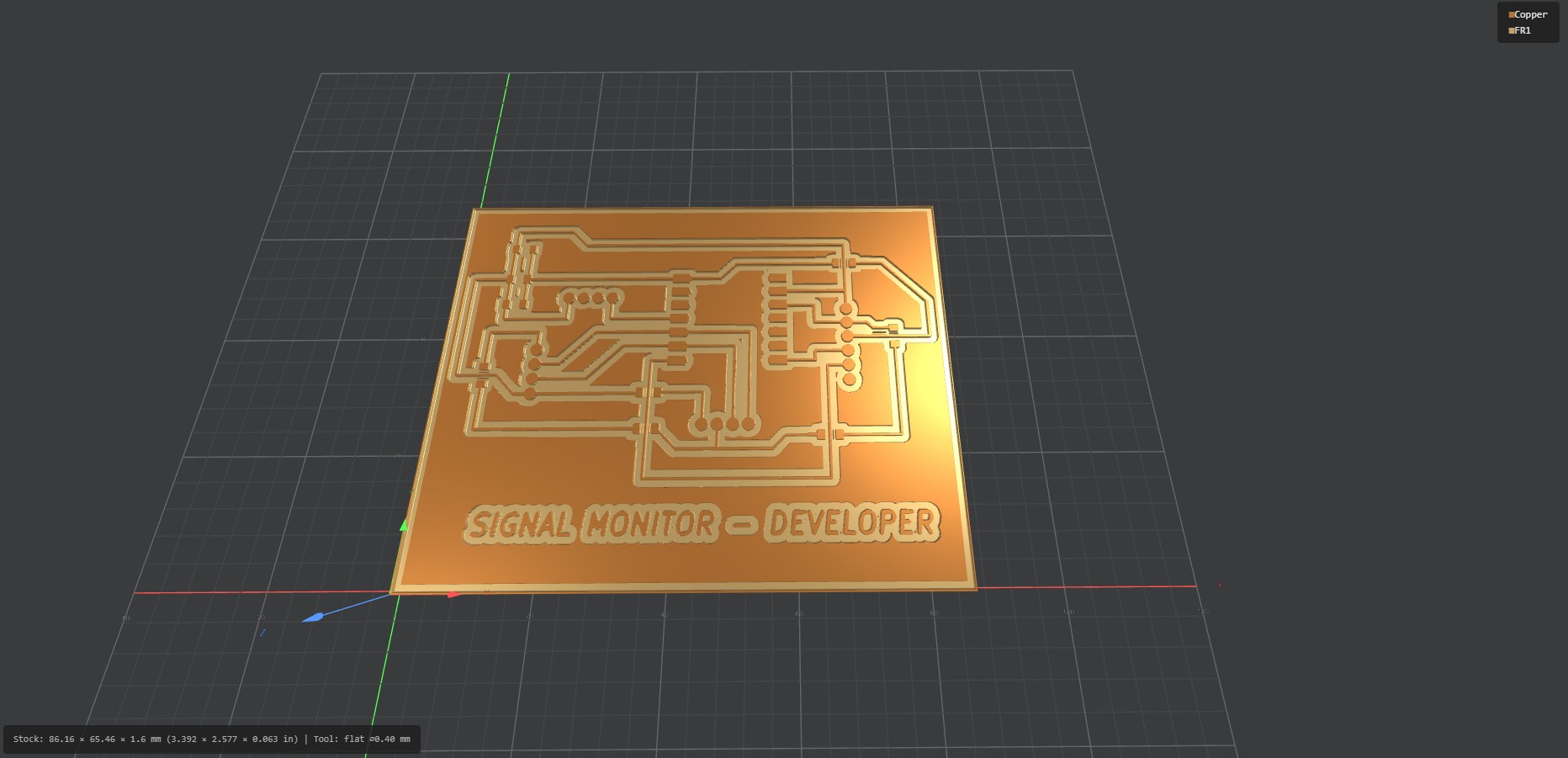
The milling process started with the traces. This step required careful setup because the tool depth and surface leveling directly affect the quality of the PCB.
Once the traces were milled, the board outline was cut. This separated the PCB from the copper board and completed the fabrication stage.
After milling, the board was cleaned and inspected to verify that the traces were properly defined and that there were no short circuits between them.
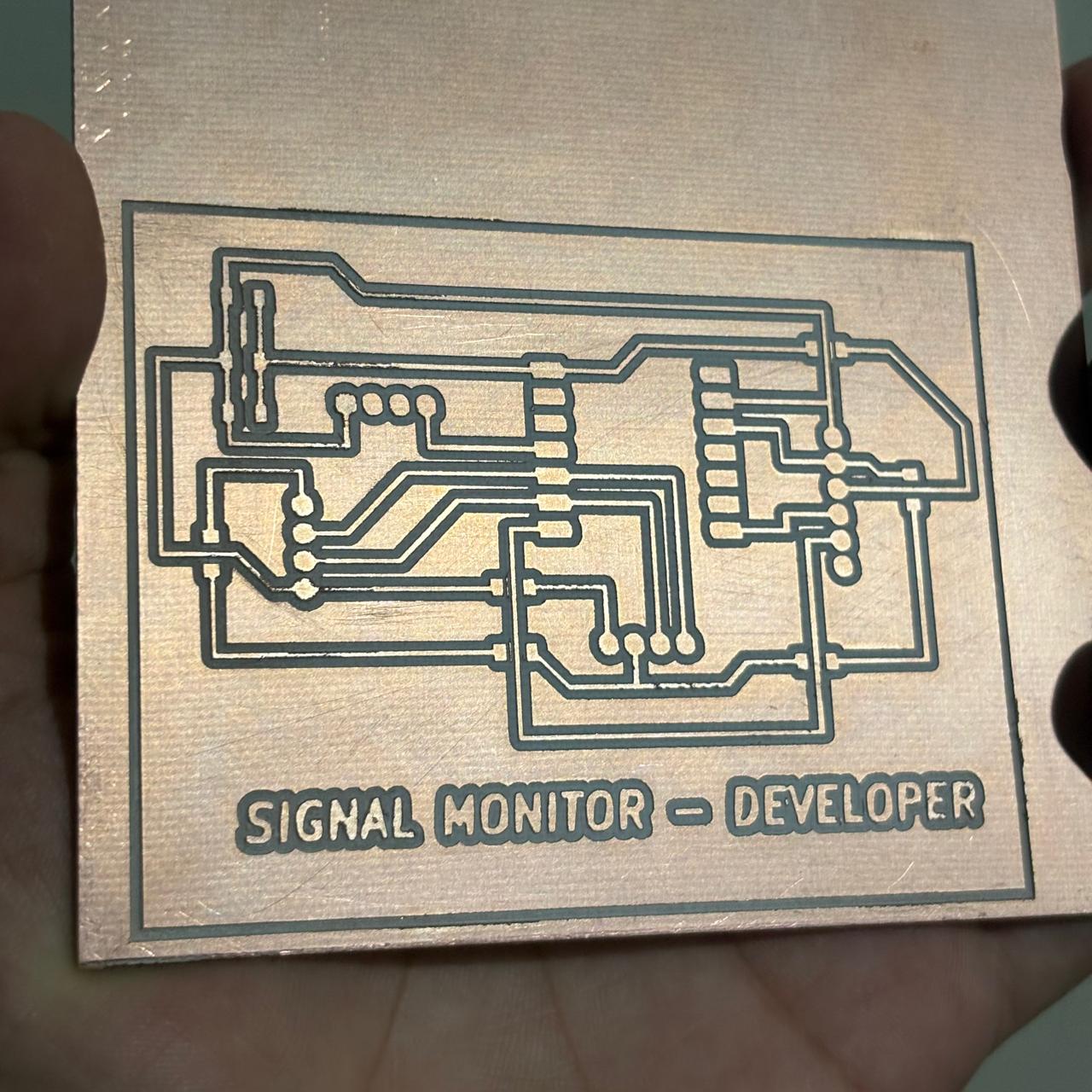
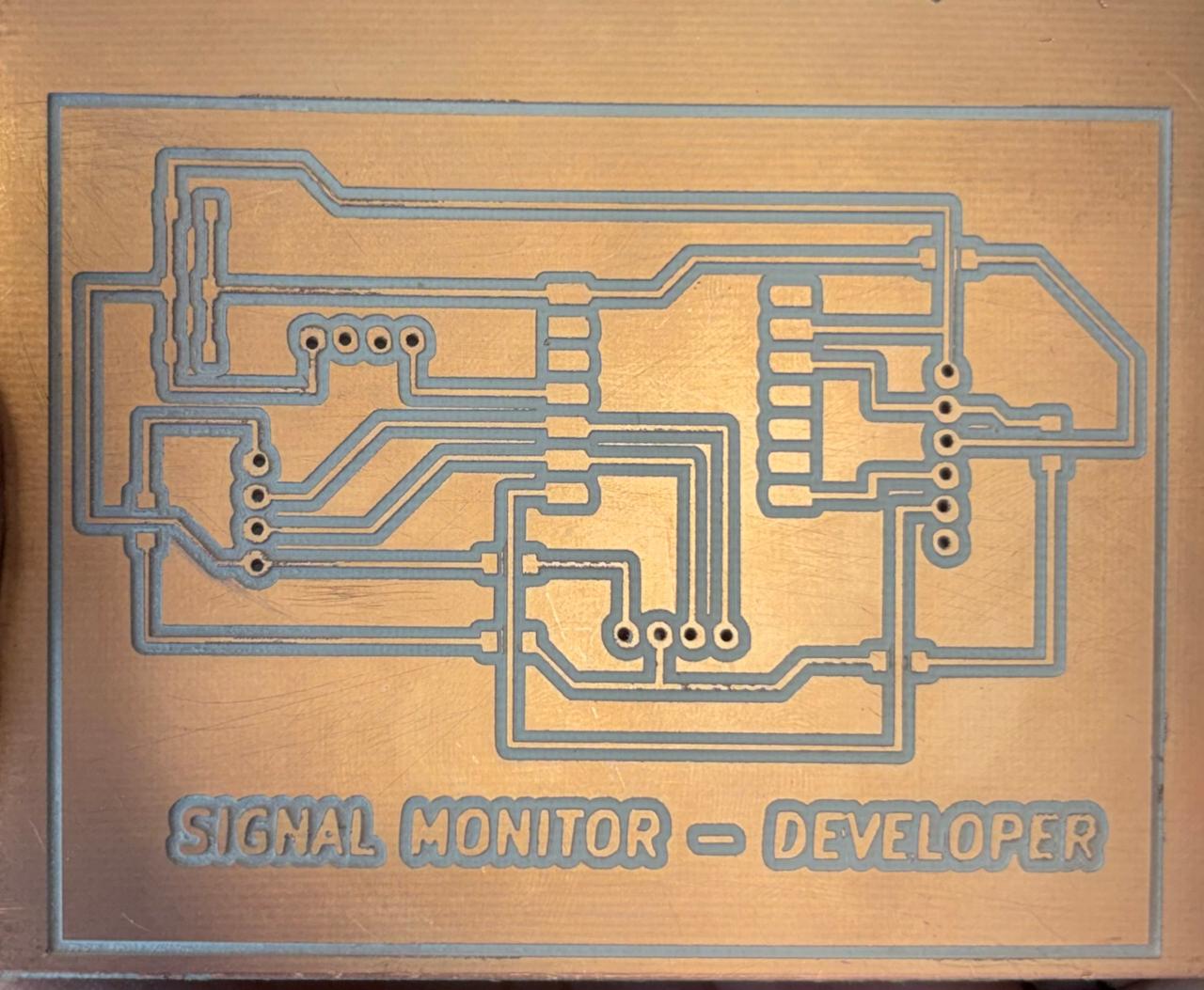
Soldering and Testing
After the board was fabricated, the surface-mount components were soldered. During this step, I checked the position of each component and verified the electrical connections before testing the board.
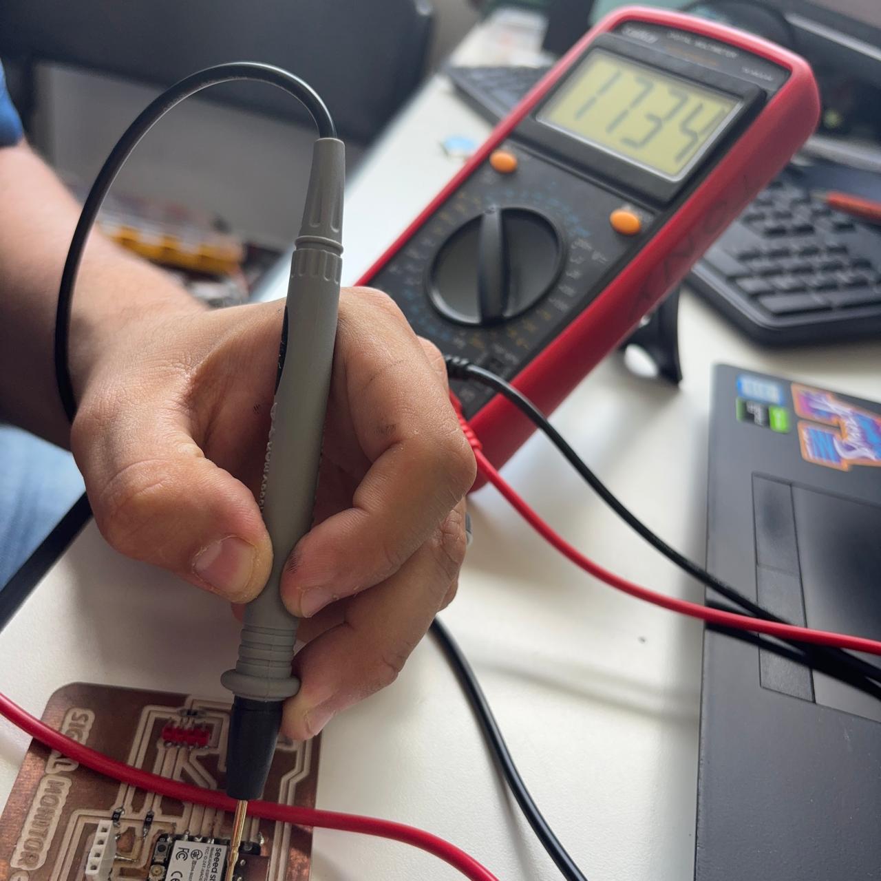
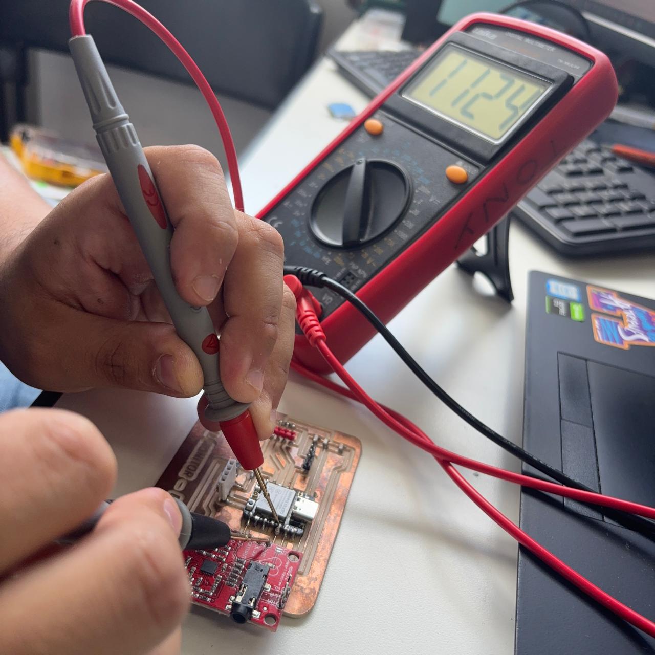
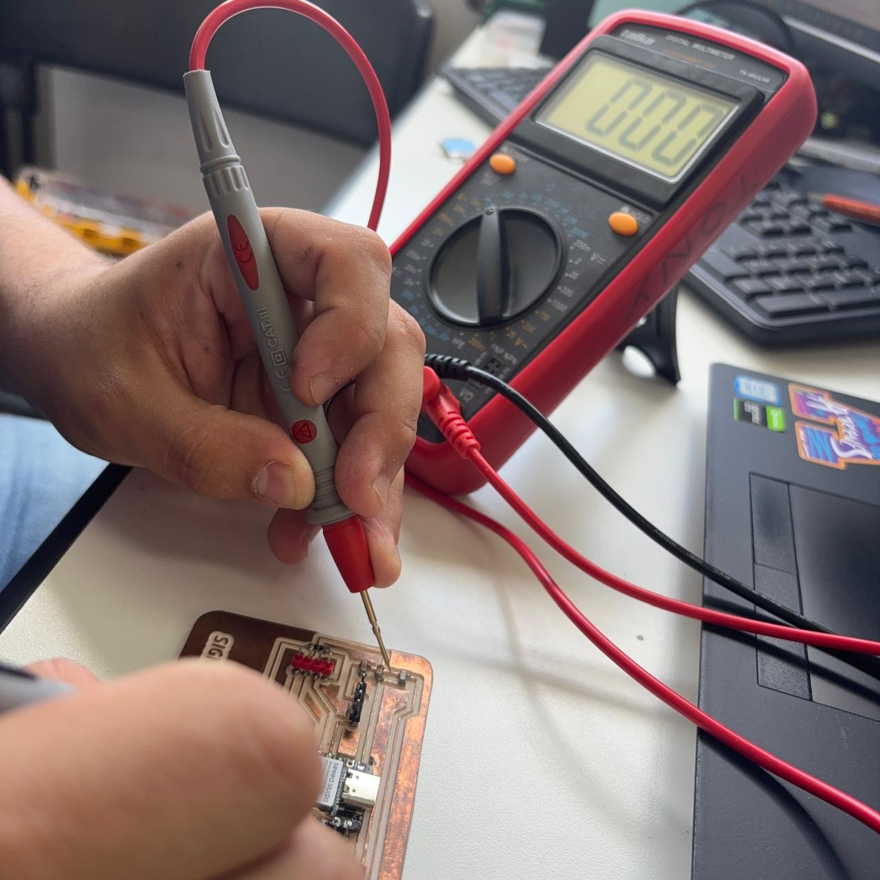
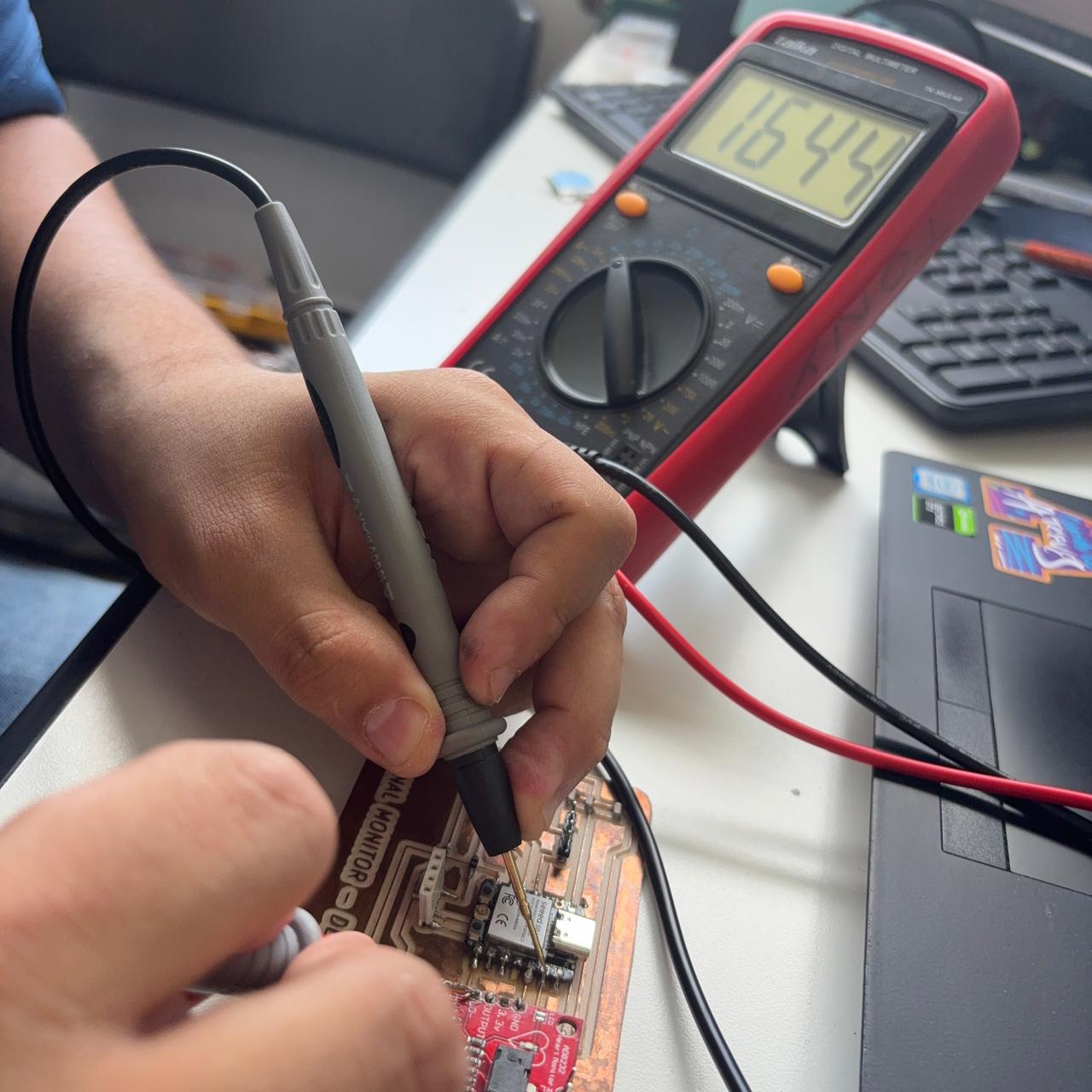
Finally, the board was connected for a basic functional test. This confirmed that the PCB was ready to continue with the input device workflow.