System Integration
link to Fab Academy class links
Individual assignment:
- Do a system integration of your final project
I had spent a majority of my time this week figuring out how to simplify my electronic design while also complicating it. A simple design would have less possible points of failure, and be easier to replace should something happen. But not all failures happen from physical damage or bad solders. Reversing wires, power surges, and electrical noise are also possible points of failure.
My work during this week can be found here week17-log.md. I am remaking this page after I finished my final project to be a more straightforward documentation of system integration.
My work with Claude.ai can be found below:
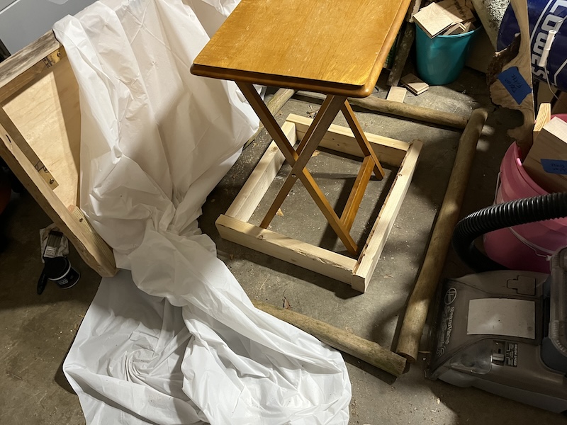
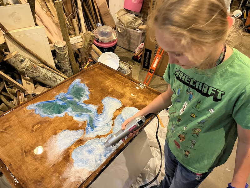
Table Top & Wire Housing
My table top needed to be both beautiful and functional by including: 1. sensors that can read the magnet in my wood turned wands 2. lights that can be seen through the table, but are hidden 3. power that can run many effects while being hidden or made into part of the show 4. pcb designs that fit into the table, and are easily updated or replaced 5. some special effects that still work if the Teacher board fails.
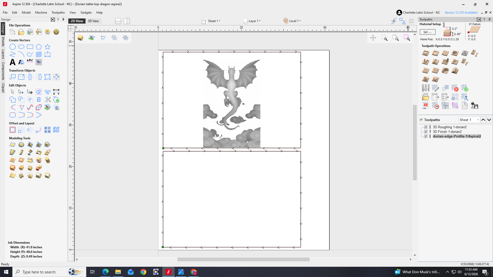
The top was cut using the Shopbot CNC. I edited my original "dragon carving file" from week 07, in Bambu Studio by using the slice tool to cut off the raised rectangle surrounding the dragon, and to squish it along the Z axis.
I wanted it thin so that I could fit electronics below, seal the back with another piece of wood.
Then I imported the new file into Aspire to create the tool paths. In Aspire I positioned the horizontal cutting plane to minimize cutting time by removing as much of the clouds and dragon I could, while maintaining the 3D feel of a dragon seen from above.
I made the last minute mistake of moving my design to the edge of my table, forgetting that I need an edge to hold the epoxy in while it sets. I should have made the cut of the table larger, and cut off the excess after the epoxy dried.
Always rethink your approach when an instructor asks, "are you sure you want to do that?"
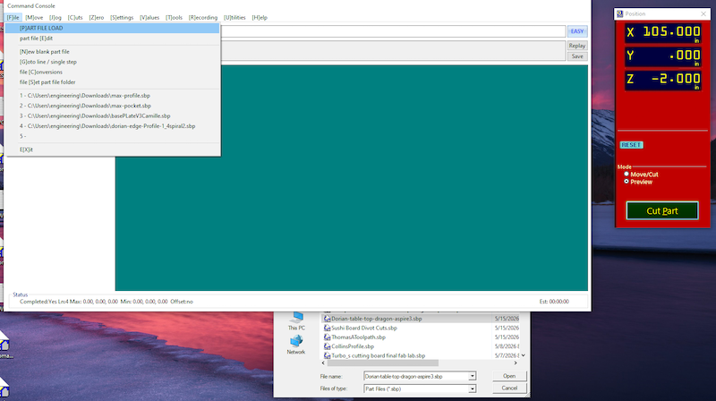
I loaded my file into the ShopBot CNC program.
I used ½" cabinet grade plywood left over from week 07. It wasn't ideal, but I thought plywood layer lines may look interesting.
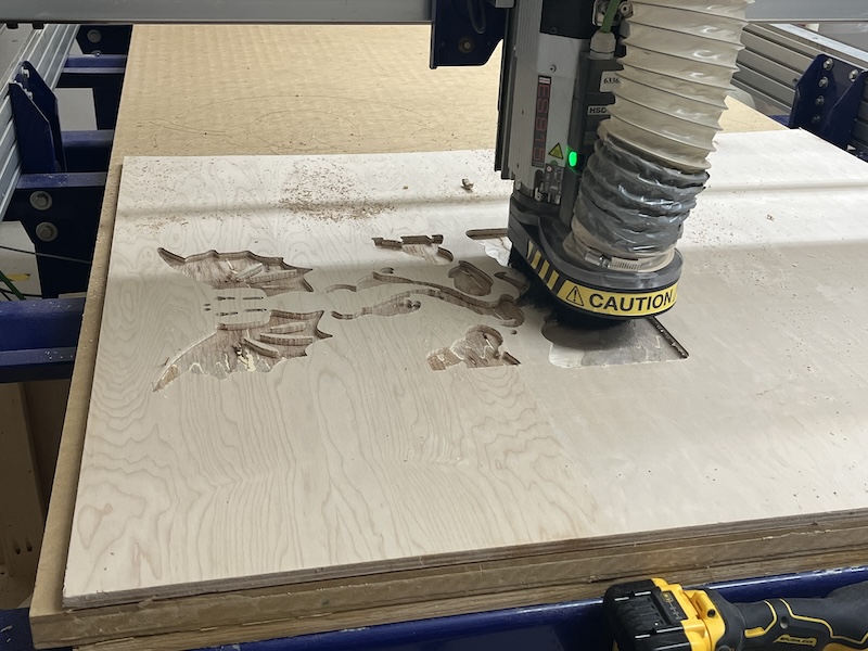
Bad idea — the plywood sheered off while engraving.
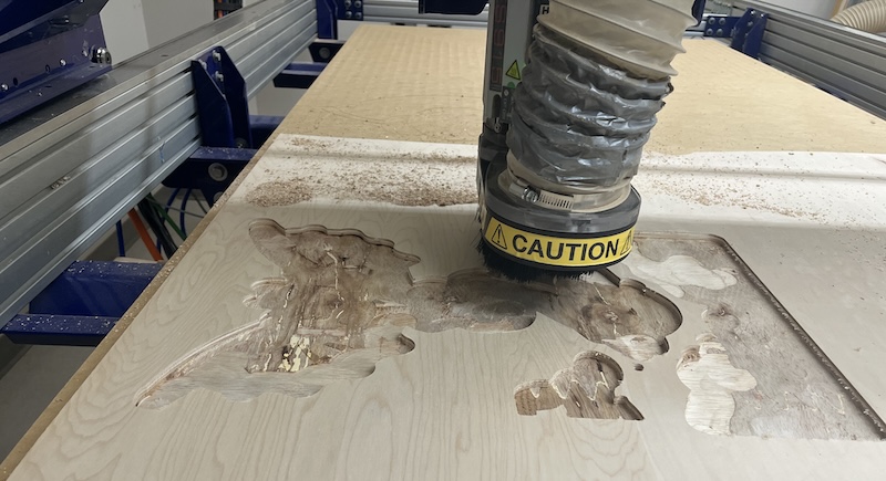
I stopped the program, and made a toolpath for the edge cut only to quickly cut out the top.
Here are my design and cut files:
Whittling
Always the optimist, I decided it was the perfect opportunity to practice whittling skills I had just taught my scouts. My apprentice and I carved out the chunks of remaining wood, and artfully extended the clouds.
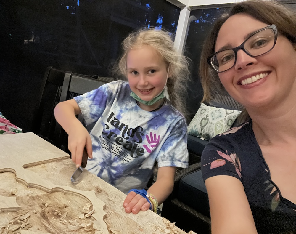
whittling knives are very sharp! Remember to wear PPE! I used cut resistant whittling tape after nicking my hand.

While we were carving, I printed the dragon file I used in Aspire. It was too large for one printplate so I divided it into pieces that would fit.
Creating the inlay
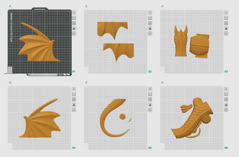 Click here for the dragon 3d print files
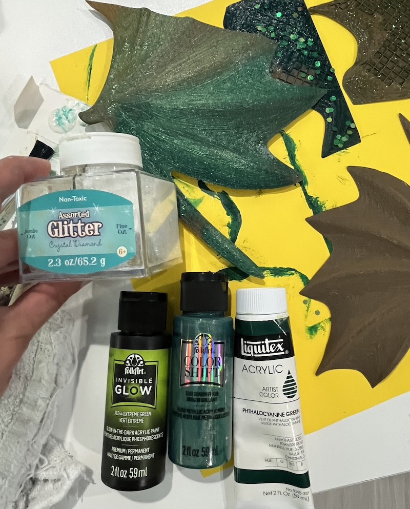
My apprentice helped me test out paints, and we decided on a base layer of dark green, 2nd coat in a holographic green, top coat highlights of glow in the dark, and a sprinkling of "crystal diamond" glitter.
The dragon's body ended up a little big, and I printed another body with a bit cut off underneath. This complicated connections, but was fine.
I also created caps for the sensors/ leds to go into. I was worried that the sensor would not be able to read through the table and epoxy well. I designed the caps in TinkerCad. The rounded conical ones were the shortest, and I ended up using them the most, because I must have chosen the deepest part of the inlay to measure when designing the file. My thought had been the conical shape would diffuse the light better than the cylinders, but I haven't tested that yet.
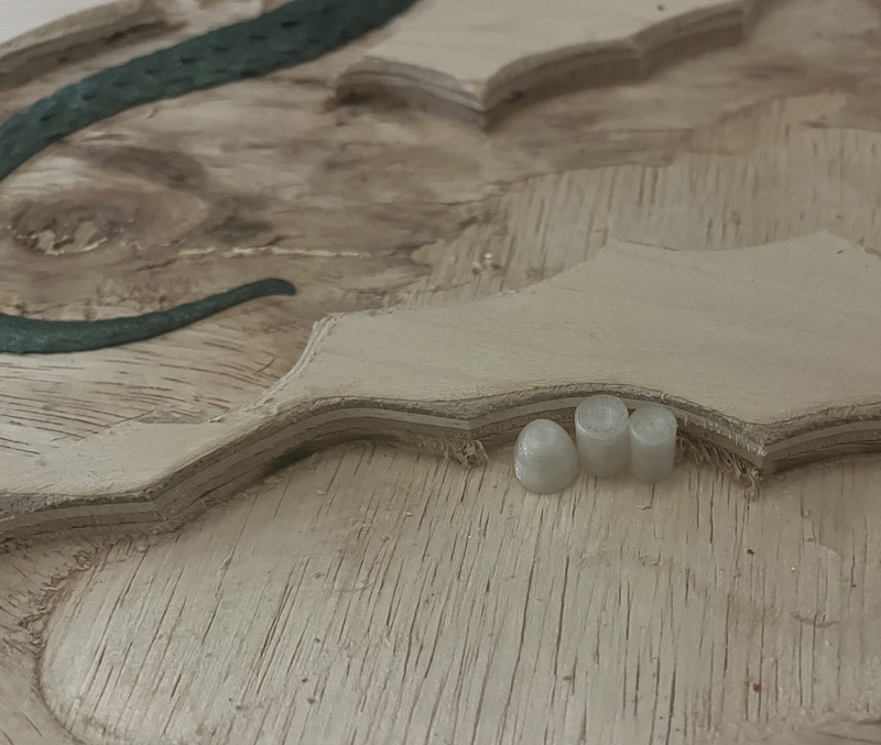
Since I removed as much of the dragon as possible, I painted the inside of the inlay as part of the dragon, and the sky. I chose to paint the inlay blue rather than color the epoxy so that I would not tint the dragon, clouds, or colored leds with blue. I sealed the back of my wood with ModPodge to seal the back in preparation for epoxy, and let it cure. Then I drilled holes where I wanted sensors, and glued the caps on top using super glue.
next time I would use caps with the bottom 5mm in height being a uniform diameter cylindrical base, and drill the holes to fit the outside diameter of the caps. This would allow me to adjust the height as needed by pushing it through the drilled hole.
Epoxy
I purchased some Alumilite™ Amazing Clear Cast Epoxy Datasheet from Michaels figuring it along with some I had at home from an attempt to learn epoxy last year, would be enough to fill the inlay. However, I didn't anticipate my epoxy having turned yellow. Although the epoxy being yellow is only a cosmetic issue, I didn't want my sky to be green.
I looked into why epoxy turns yellow, and how to prevent it. The yellowing is caused by UV light breaking down some bonds within the material.
I guess I will not be shining UV light on to my dragon to make it glow lest I turn my sky green!
Some resins are UV resistant so they stay clear longer.
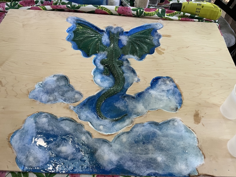
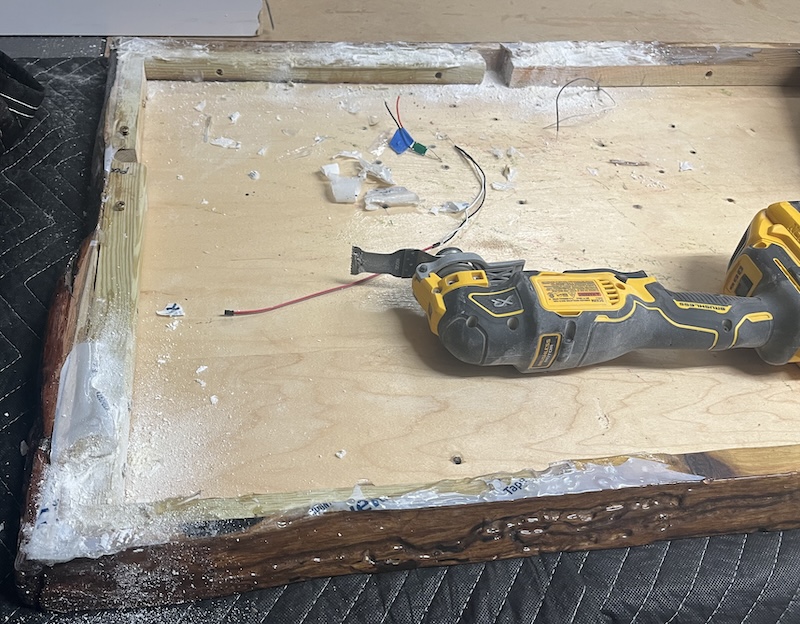
To seal the wood so that bubbles don't enter the epoxy as it sets, I painted a thin layer of clear epoxy resin into the inlay over the paint. I added a very thin layer of white batting to make fluffy clouds to add texture and depth while hiding the sensor caps, string lights, and wireless transmitter. I also painted the wire of the led lights and the transmitter to match the background paint.
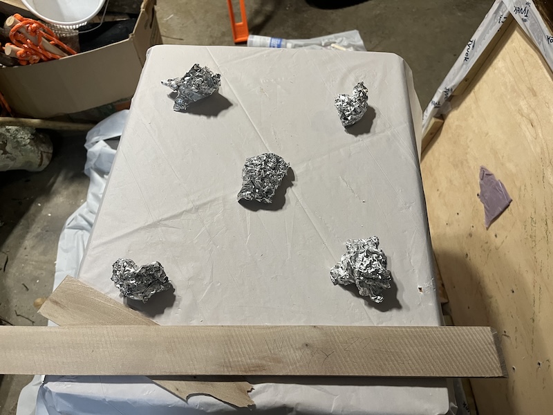
Now I needed a solution for pouring epoxy in my open inlay. I read that wax paper does not stick to epoxy. So I took wax paper (not parchment paper) and tinfoil, stacked them together, and folded them longways twice. I then taped the folded stiff wax paper to the board.
It worked really well, and peeled off easily. The tinfoil added the stiffness to keep the edge relatively straight. I used my planer to take a little extra epoxy off to make it flush.
I made sure to skim my large level over the top in both directions to make sure all the sensor caps were below the top before filling with epoxy. However, somehow they ended up higher than the inlay! None moved, their glue seemed to hold.
I needed to raise the height of my table top. David suggested flooding my top. I definitely did not have enough epoxy to flood the top. I chose to get a different type of epoxy that would be more resistant to yellowing, TotalBoat Table Top Epoxy Resin, Datasheet. It was also less expensive, and could be delivered quickly.
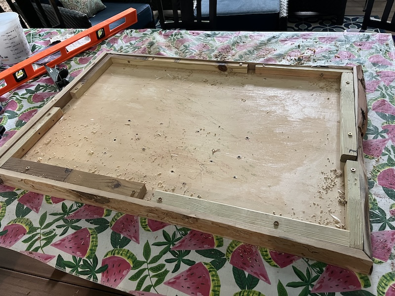
Framing my table top
Furthermore the edge of plywood is not pretty, I planned on using a veneer around the outside of the table. I would have added blocks or a cutout to add the height and support needed for the components to fit, and added the veneer so that it overlapped the bottom by the width of the bottom plywood. Then the bottom piece of plywood that I had cut would be secured on the bottom creating a removable back.
However, I did not have veneer. I did have scraps of sweet gum live edges that I saved from my remodel! I used those to create an edge around my top.
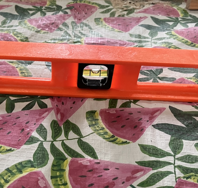
I attempted to offset the sides to compensate for the height of the sensors by first making sure my table was level.
Then I created framing around the edges of my top using scrap wood.
It helps to plug in the saw!
I learned when I made my scrap sweetgum table, that I needed to use construction screws with a star tip! The star tip spreads out the force along more surface area so that the screws are less likely to strip. These screws also have an unthreaded part near the top. This is for screwing together 2 pieces of wood. After the threads are through the first layer of wood, they grip the second while sliding in the first. As you tighten the screw, the bottom piece is then pulled tight against the top piece.
While I did have the correct type of screw, I did not have the correct length!
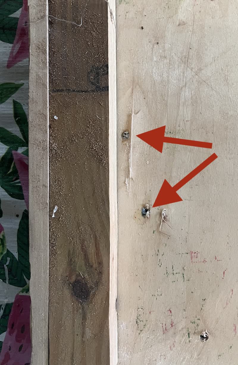
I backed the screws out where ever they were too long, and hoped I could remove them fully after the epoxy was set.
I also managed to cover 2 sensor openings with the framing.
I did have one miscut that made one side slightly shorter than it should have been. However, as it was live edge, some parts were thicker than others, and the corners didn't match up anyway. I took advantage of the width of the miscut live edge piece, and trimmed it on an angle to make it longer. I did this on my bandsaw though, so it was not straight. With my hand planer, and sandpaper I was able to get it pretty close.
I had to keep telling myself, "it is just the prototype," over and over again
I should have filled the corners in with wood filler! I'm planning on using some filler, and uv setting resin to fill the corners in at some point.
Cleaning before finishing
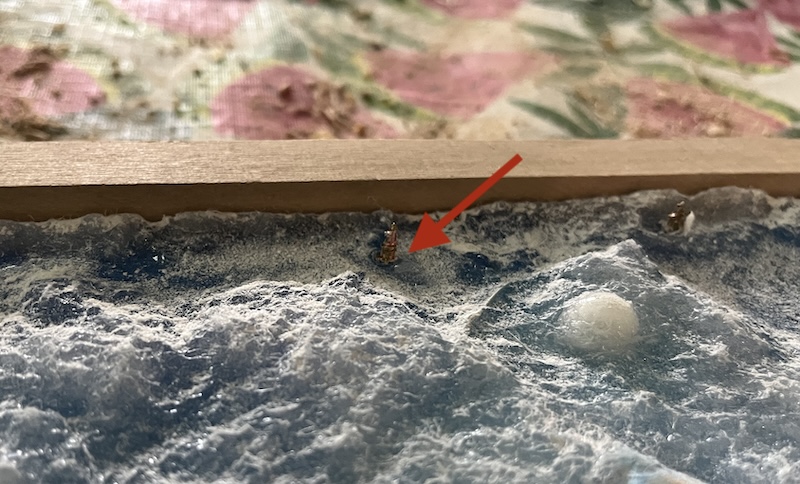
- I cleaned out the debris left from the bugs that created the lines in the wood using a toothbrush.
This wood was kiln dried, and is safe to use.
Multiple layers of epoxy
When applying multiple layers of epoxy follow these steps to ensure the epoxy adheres properly.
If the epoxy is dry:
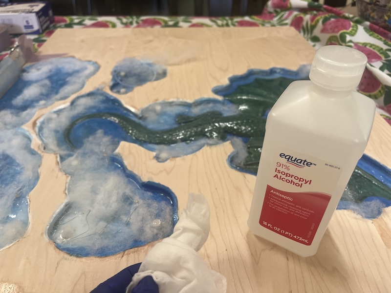
- Scratch up any dried epoxy with sandpaper, vacuum the dust, and wipe with isopropyl alcohol.
If the epoxy is not fully set
- follow manufacturer's instructions
- wait until the epoxy has set for manufacturer's recommended amount of time
- it should be firm enough to hold the next layer, yet still tacky.
- pour another layer directly onto the setting epoxy.
I was thrilled when I learned that I didn't have to wait a day between pours. Better bond, no surface prep, and faster! Not only was it going to pour with rain over the weekend, but I was leaving for a wedding the next day!
Staining
I was trying to be as quick as possible, but stain needs to dry before you can use epoxy on it. Oil based stains take 24hrs or more to dry, gel stains even longer. Water based stain was my best choice, but I didn't have any in my random collection. It ended up taking me longer to get the waterbased stain, and use it than the dry time on the gel stains would have been. Oh well, next time I will use what I have.
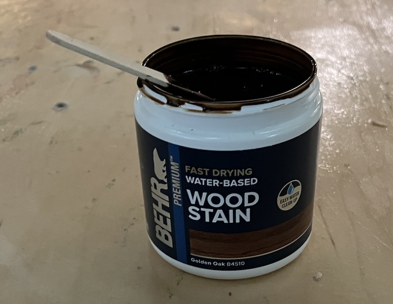
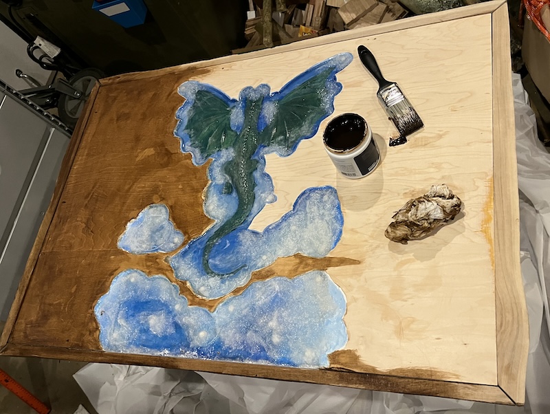
I should have stained the wood before doing any resin work! But I didn't. I tried to sand off the drips of epoxy that fell outside of the inlay while I painted on the first layer of epoxy. It didn't work, and the stain would not penetrate in those areas.
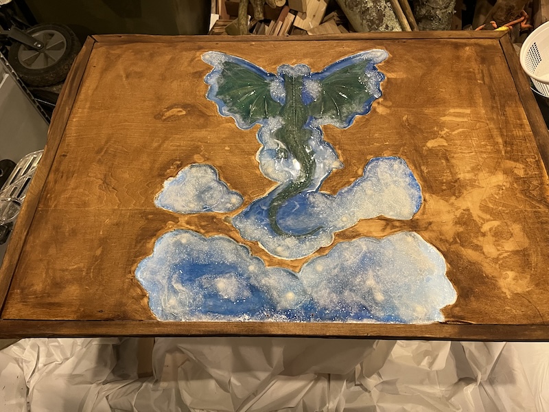
I learned from a previous project not to stain the bark! It is already dark, and absorbs more stain than the rest of the wood.
Prep for epoxy flooding
I prepared a small area in my garage that would not be disturbed for the weekend. I couldn't leave it on the porch as it would be pouring all weekend. Luckily our garage has our heat pump water heater that keeps the temperature and humidity down!
Garages are not level! This prevents water from pooling in your garage after driving in from the rain.
So I first leveled a small table. Then I surrounded the table legs with 2 rectangles of scrap wood. One close to the legs of the table and one a few inches larger than the size of my magic table top. Next I covered the table and the scrap wood with plastic tablecloths. In doing this I created a moat to catch any epoxy drips, protecting both the folding table and the floor.
Next I needed to make sure my table top was level.
Never trust that just because the table you are using is level that your item is level!
I was having a lot of difficulty trying to level my top, because of its size. I came up with the idea of using aluminum foil. I scrunched up, not too tightly, some foil, and placed them under the table.
Then I was able to apply pressure where needed to adjust the table top, and the foil held its shape while supporting the top.
Flooding the top with epoxy
To make the most of the epoxy I had, I used the yellowed epoxy on the wood part of my table as the first paint coat, and it wouldn't affect the color. I then made a large batch of epoxy, 1:1 ratio by volume for both brands.
do not mix epoxy brands when combining part A and B. Once combined according to manufacturer's instructions, you can mix epoxy brands.
I did not mix the liquid epoxies. I did layer them on top of each other.
I knew my corner joints would be where all the epoxy would leak, and I did not think my wax paper trick would work in this situation. I bought some Tyvek tape while picking up the water based stain, and handy mixing buckets (they have offset measurements so that you can accurately measure your second ingredient!)
I used the Tyvek tape to seal the cracks where the sweet gum live edge pieces met the plywood.
Then my apprentice helped me mix and pour the epoxy.
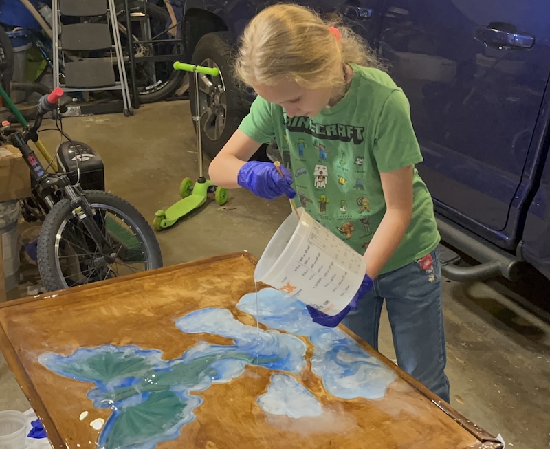
I was frustrated with trying to use a stir stick to spread the epoxy, and grabbed the new, cheap, bent angled icing spatula I had gotten for a different craft project.
Bent angled icing spatulas aren't just for cake!
Adding Mica Powder
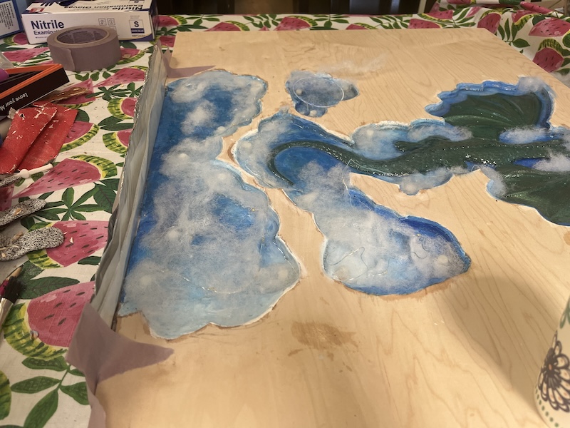
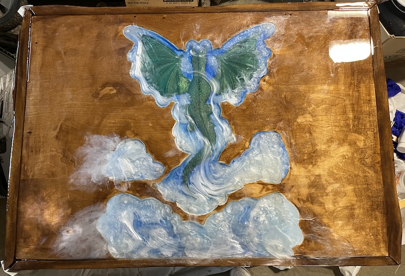
Next I wanted to add white mica powder to some epoxy to make cloud like wisps and puffs. Not only would this be for artistic beauty, but for additional coverage of components, and hopefully aiding in dispersing light.
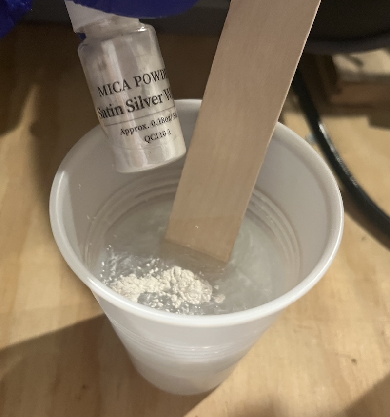
I only made a little white epoxy. I wanted it to stay mostly in the inlay, and spill out a little onto the wooden top. I envisioned wisps of clouds creating a connection from the wooden top to the inlay. Symbolically the wood of the table represents reality, the inlay represents the fantastical, and the wisps of clouds would be magic tying them both together.
Quite fittingly, just as reality never truly aligns with fantasy, my wispy clouds can't quite make the connection work either. They ended up making the table top look foggy.
I did learn that there are different types of epoxy. The one I was using is for thin even coats. There are others made for creating wave effects. I think it is more viscous so that it doesn't spread as much.
We used my hot air gun to pop bubbles and create swirly clouds.
I gathered the drips before they fell, and redistributed them along the live edges where the epoxy was not reaching.
I could only do this for a little bit, as I had a plane to catch!
When I returned the epoxy was set!
Cleaning off epoxy
The Tyvek tape worked really well,
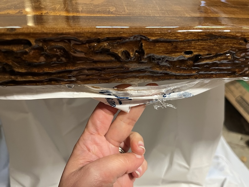
except where my wiping the drips accidentally caused a coating to form over the tape.
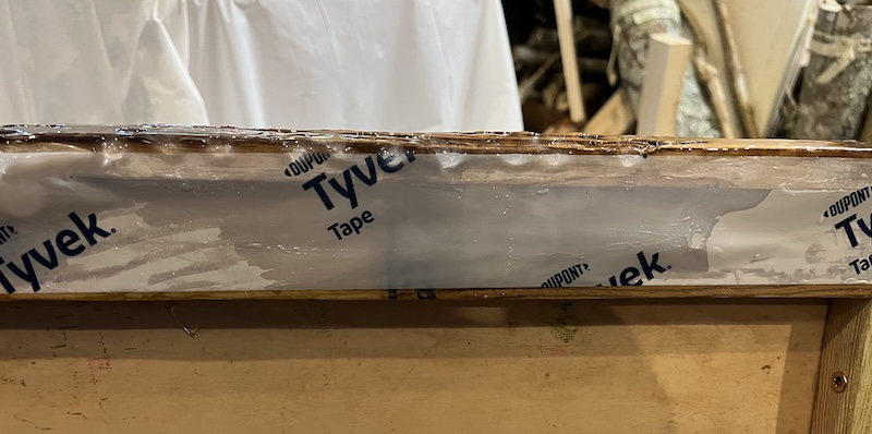
The tape was encapsulated in the epoxy. I was able to pry most of it off. I brought it into the FabLab that week to ask for advice. Barbara suggested I cover the bottom in material. Zack suggested a chisel or the oscillating multitool we use to cut tabs on the Shopbot. I used the oscillating multitool, and a chisel, keeping the fabric as a last resort.
Making a back to enclose the wires
Originally I had planned on using a second piece of plywood for the bottom, using spacer blocks to separate the 2 pieces, and adding a veneer to the sides, but since I was using the remnant sweetgum live edge as my frame the top and bottom would have been really close to the electronics.
This may have ended up being fine, but I wanted to have some room for air circulation should any component need room to cool.
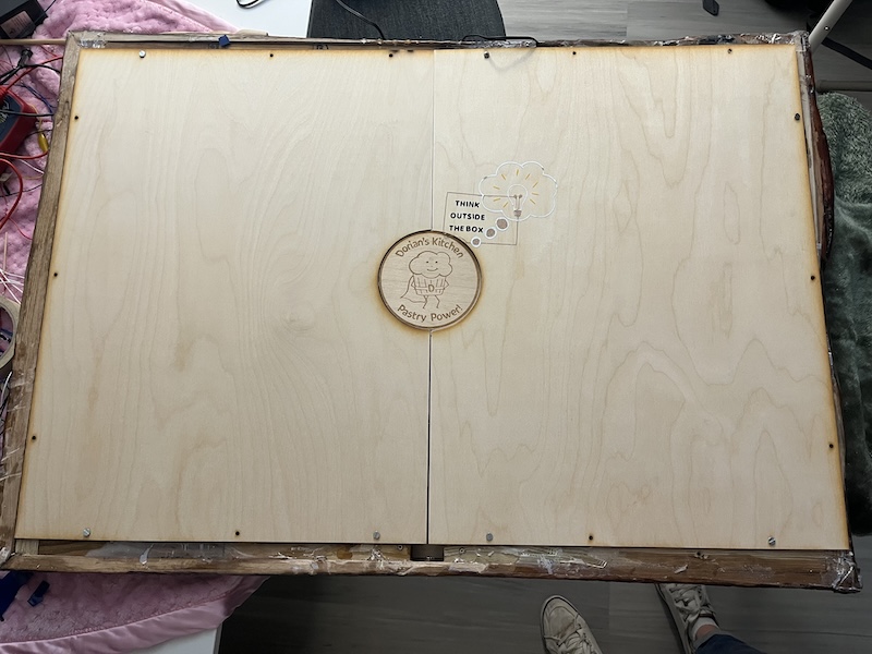
So I made a simple file with CorelDraw to lasercut a back that had precut holes to make screwing it onto the top easier. I wanted to have a piece that would allow easy access to the Teacher board that could be hidden. A random circle cutout would be suspicious so I engraved my Pastry Power Super Cupcake logo so that the cut would look like the border.
I used washers, magnets, and a larger circle to mount the circle, it works, but needs improvement.
I used 2 pieces of 1/8" plywood since the design was too large to fit on one, which meant I could not laser engrave the center circular cutout as it would be in 2 pieces. Instead I copied the hairline cut for the center hole, and created a second file engraved with my pastry power logo. I cut that out on scrap wood.
I was off by 1" when making my file. I must have accidentally used the measurements of the fabric my scouts were cutting for their Bronze Award Dog Bed Project. We had a booth at a big Animal Shelter Fundraiser event to raise awareness for our project, and encourage people to make beds themselves. I hadn't realized this until I used a cut blanket to protect my table top while working on the back, and noticed it fit exactly! Here is a link to my troop's how to video. I encourage you to reach out to your local shelter to see if there are ways for you to help.
laser cut files:


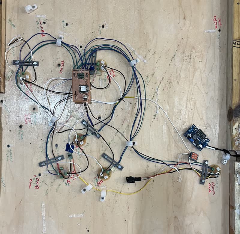
Wire Management
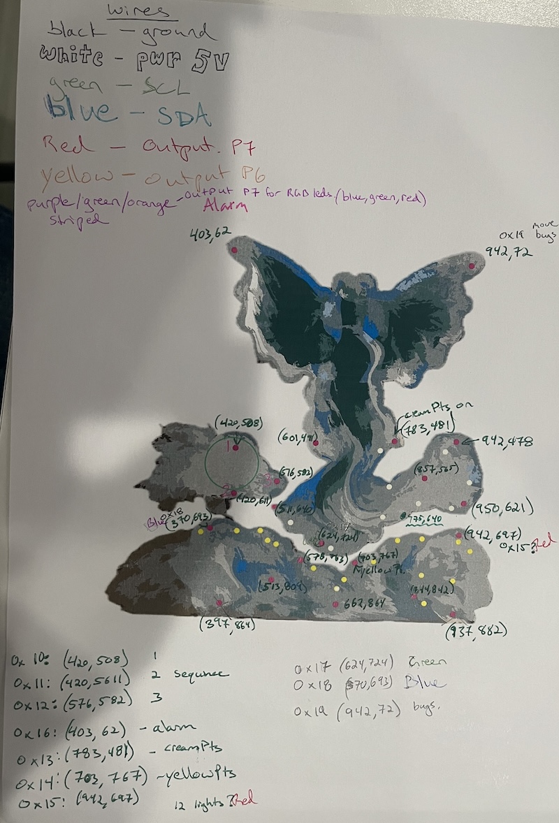
Inside the table top, I labeled my sensor caps, and created a sensor map for my processing user interface.
I spent a day laying out my wire design using color coded yarn.
This allowed me to easily fix mistakes, like attaching all the rgb leds to ground instead of power, before cutting my wires.
I tried to create common ground, power, and I2C bus stations for the nodes to connect to, but had to scrap that idea when the teacher couldn't read the nodes. I believe this was because of noise caused by the common power and grounds being connected directly to the voltage regulator and not the close enough to the 100uF polar capacitor in series with the 94nF capacitor.
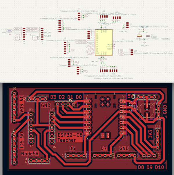
Luckily, I had designed my teacher board to have all nodes connect directly to it. A future spiral design will increase my teacher pcb to allow more nodes to connect. The ESP32-C6 can handle 112 nodes communicating through I2C connections. (the datasheet says more, but in practice I have heard to only use 112 max).
I wonder if I could connect more if I gave more than 1 ATtiny the same name, and were only to receive orders not send a response?
My electronics were connected using color coded wires.
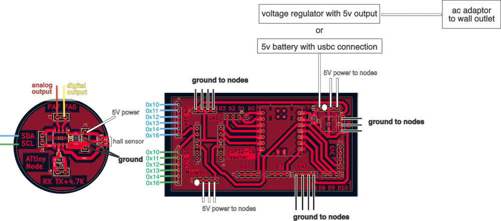
Each ATtiny node has the option for an analog output, red wire; a digital output, yellow wire; SDA, blue wire; SCL, green wire; 5V power, white wire; 2 ground connections, black wires, and a jst connection for programming through RX and Tx.
0x10, 0x11, 0x12 are the nodes in charge of my Power Spell sequence 1, 2, and 3 respectively. They all had a red led and 1K resistor connected to P7 analog output as a last minute change so that I could see if they were triggered.
0x13 controls the cream colored led string directly surrounding the dragon from its PA7 analog output.
0x14 controls the yellow colored led string directly in the bottom cloud from its PA7 analog output.
0x16 controls the alarm from its PA7 analog output, and the wireless transmitter from its PA6 digital output. (It is the only node to have a special code. It was added at the end of the project as my first spiral. Previously it had just run the wireless transmitter as a regular node.)
0x15, 0x17, and 0x18 will control the red, green, and blue legs of a bunch of RGB LEDs respectively. These LEDs will fill the empty sensor caps until they are needed.
I connected the nodes to the teacher board with the SDA and SCL wires attaching in node number order so that I could easily troubleshoot. (0x15, 0x17 and 0x18 are for a future spiral.)
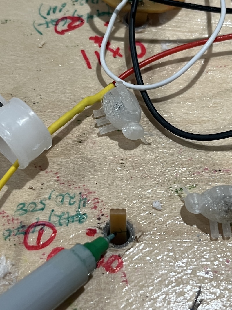
For wire management, I used cable clamps and 3d printed wire holders that secured the wires more firmly, which helped to hold the nodes in place while keeping the wires secure.
I used JST connections with the RX and TX connections on the ATtiny412 nodes, as well as the power and ground connections. I would have liked to use them for all connections, but I ran out. The lab had screw terminal blocks, but while they were good for initial prototyping, because you can easily change the wire placement, they kept coming loose!
jst.co.uk jst connectors Matt Millman's page "Common JST Connector Types is very informative. It explains types of wire connections, and the tools needed to crimp wires for JST connectors.
When using terminal blocks check how the wire gets attached. The side closest to the screw is where the wire goes on ours, but the wires fall out with enough movement either way. I want to use a glue to prevent this, but then I can't remove the wires.
Click here for my 3D printed wire holder file
I plan on making another teacher board that has more connections to the power, ground, and I2C bus, but for now I had enough connections to make the nodes I used work. When I remake the teacher board I want to use JST connectors aligned in rows, organized by node that connect to the power, ground and I2C.
PCB design
I had several versions of my PCB designs, and I am sure I will have several more as I continue to tweak the design. My final designs are shown here:
ESP32-C6 teacher:
ATtiny412 student node:
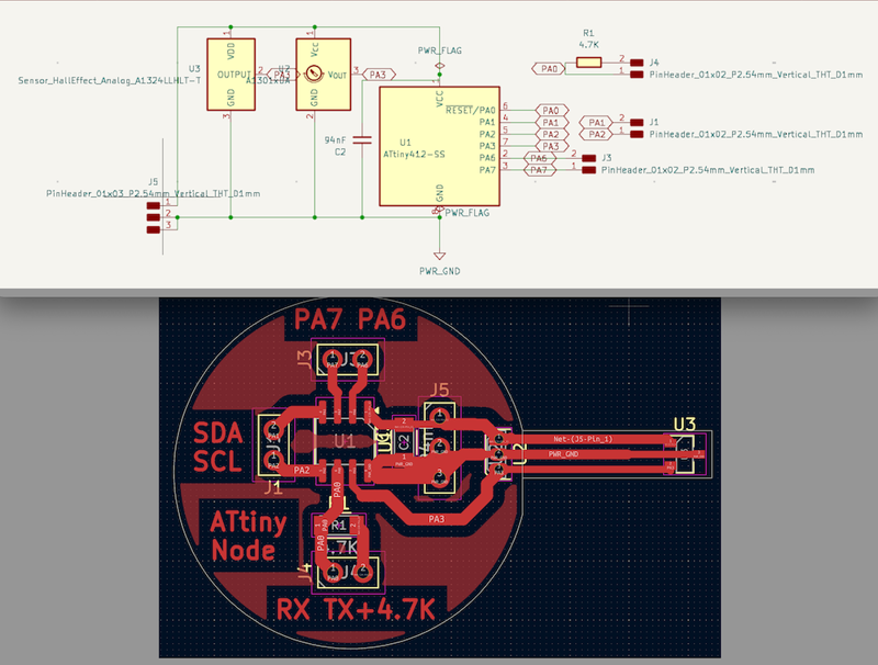
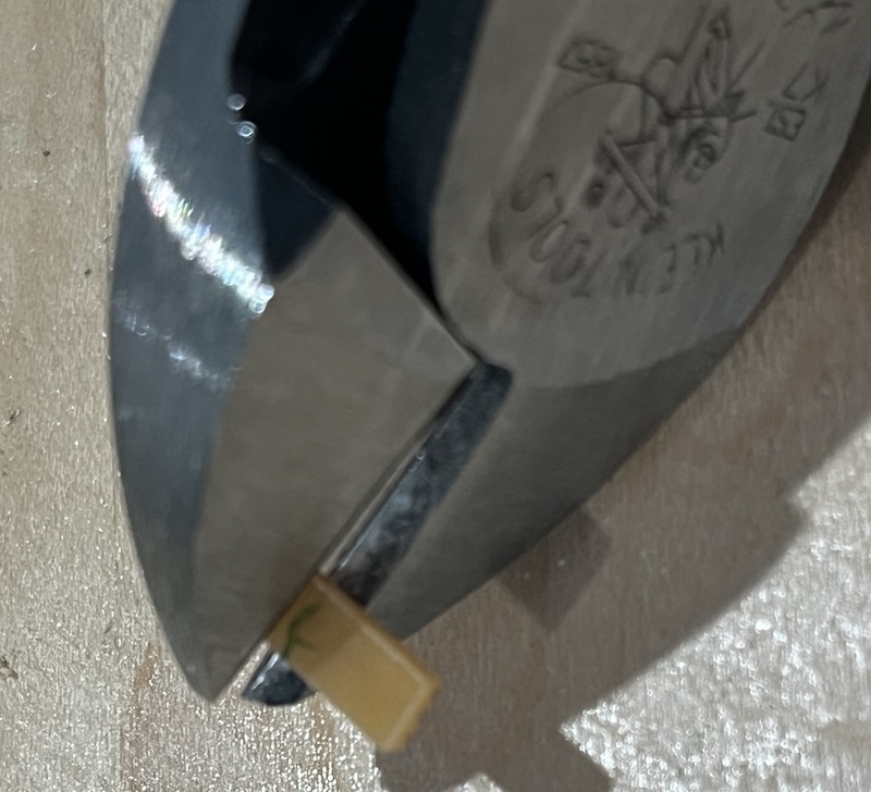
The protruding part of the ATtiny412 node gets cut when making the PCB. I did this by making the cut line in a different level than the edgecut, and making a toolpath just for that cut.
It allows for a surface mount sensor to be mounted in the sensor cap on the table. If the sensor remained surface mounted to the PCB, I do not think the sensor could be read reliably.
An even better use of this piece is to mount the through hole sensor flat onto it,
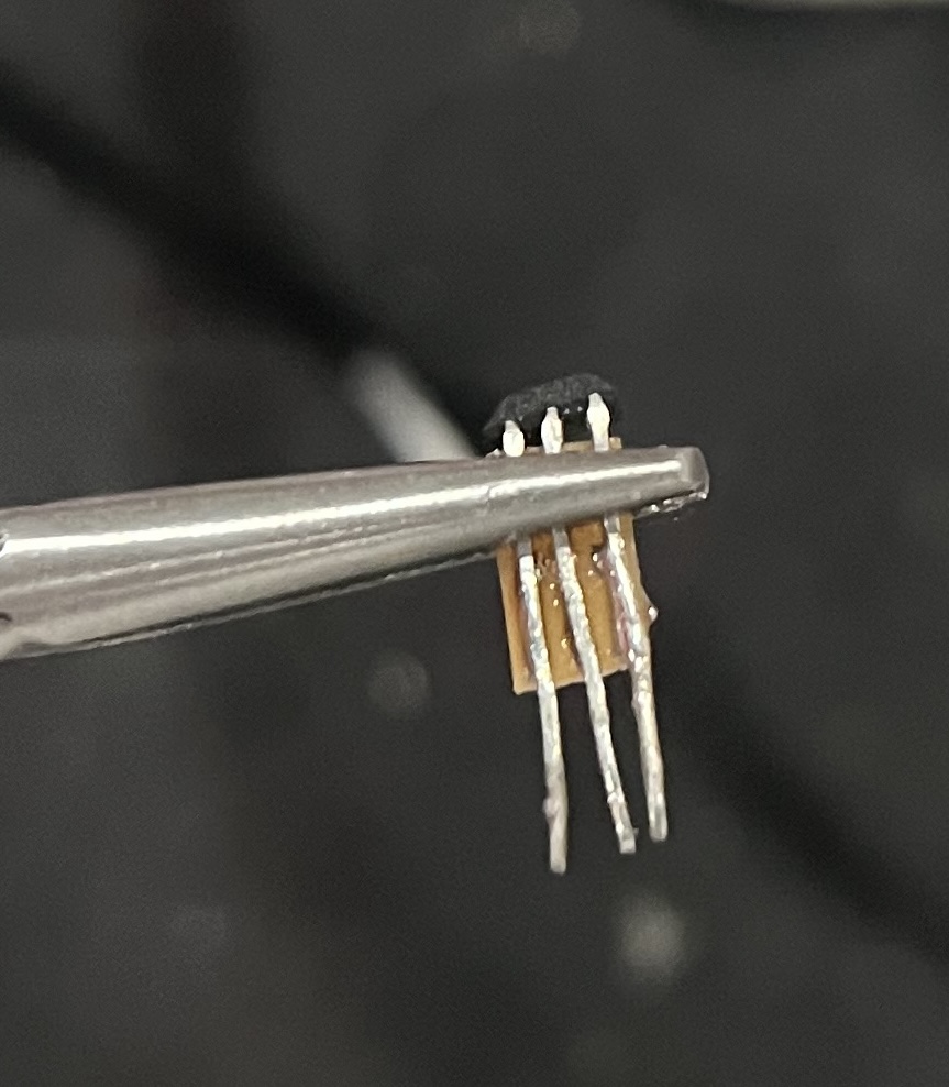
then attach it using the protruding legs in the through hole mounting holes. The PCB piece then acts as a support, and can be secured to the main pcb board with glue or epoxy. It also prevents the legs from touching!
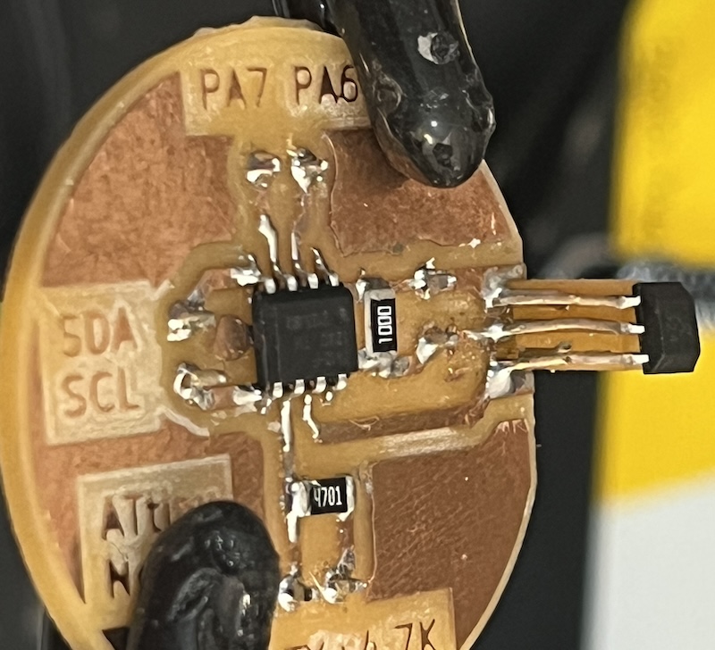
I ended up removing the switch pcb that I talk about in week16-log.md, because I used an ATtiny node as the switch instead. The ATtiny nodes run on 5V, and the switch was needed so that the ESP32-C6 could turn on the power a component that needed the full 5V. Should I add a motor or another component that would have a significant current draw, I will add the switch back again.
Power
My table can be powered in multiple ways
- It is hardwired to be powered by a 9V AC power adapter plugged into a wall outlet. It is attached to the voltage regulator.
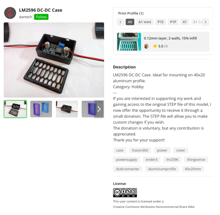
I made sure to adjust the voltage to read 5v before I plugged everything into it the first time. The device was then placed into a 3D printed case. This prevents the potentiometer from being bumped, which may fry all my electronics.
I found this LM2596 DC-DC Case by danbtech on bambu studio, but had to adjust the size, and cut out the internal supports.
I could also add a TVS diode wired in parallel before my common 5V rail like I originally planned. I was told this was not necessary though, and at the time I had planned on using a rechargable battery.
For a future change, I will add a junction pcb board for where the power connects from the ac adapter to the voltage regulator, and out to my teacher board. On it I will have a (TVS diode, a speaker, an led, and resistor in series), in parallel accross power and ground coming from the voltage regulator. That way I will hear and see if there is a voltage spike. I could add a fuse as well so that I could continue once it resets.
-
The USB-C connection from my computer can also be used, but only because I don't have many nodes attached, and they don't spike or pull too much current. I am more worried about damaging my computer than the Teacher board as I have added 2 capacitors in parallel immediately after the power input
- 1 ceramic 100nF decoupling capacitor to reduce noise
- 1 bulk capacitor 100µF electrolytic capacitor to prevent damage from current spikes
-
A rechargable battery pack connected through USB-C was what I originally planned for. It could be hidden inside my table during performances. The only thing I may need to add is a small system constantly drawing current so that the battery does not turn off should my nodes not draw enough with the sensors. I'm sure I can make a little creature to leave on.
It is safe to plug a 5V battery pack into a XIAO ESP32-C6 to power the 5V rail as the 5V pin is the common power rail.