3. Electronics Design
3.1. Idea
This week I learned some PCB design techniques .
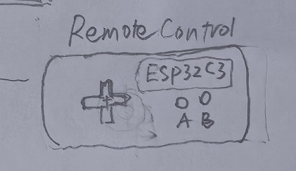
As my final project involves a wireless controller. I would like to make a controller pcb to verify my final project idea.
I use LCEDA (pro.lceda.cn) for schematic and PCB design.
3.2 Electronics Design
3.2.1 Componet list
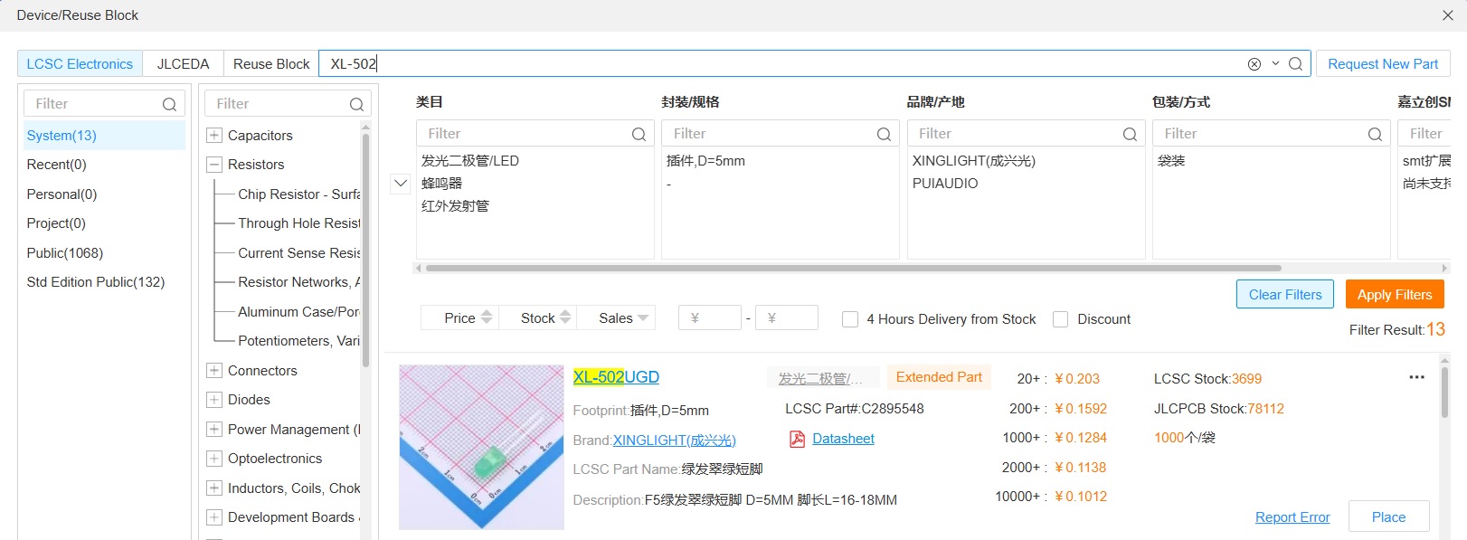
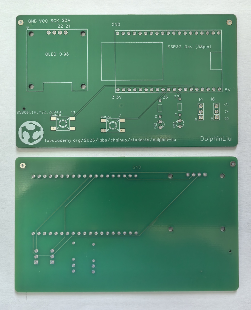
I use ESP32 microcontroller, 0.96-inch OLED display, resistors, LEDs, push buttons, and a 3-pin expansion header.
- Here is the component list:
| Component | Value/Type | ESP32 Pin Connection |
|---|---|---|
| Button A | — | GPIO13 |
| Button B | — | GPIO14 |
| LED 1 | Resister 500Ω | GPIO26 |
| LED 2 | Resister 500Ω | GPIO27 |
| OLED | SCL | GPIO22 |
| OLED | SDA | GPIO21 |
| pin header 1 | — | GPIO18 |
| pin header 2 | — | GPIO19 |
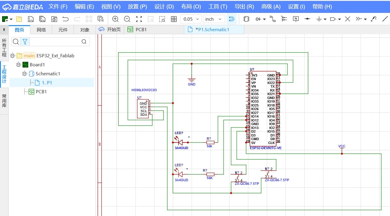
3.2.2 Schematic Design
I use "File ->New -> Project" to create a new project in LCEDA,which containing both schematic and PCB files.
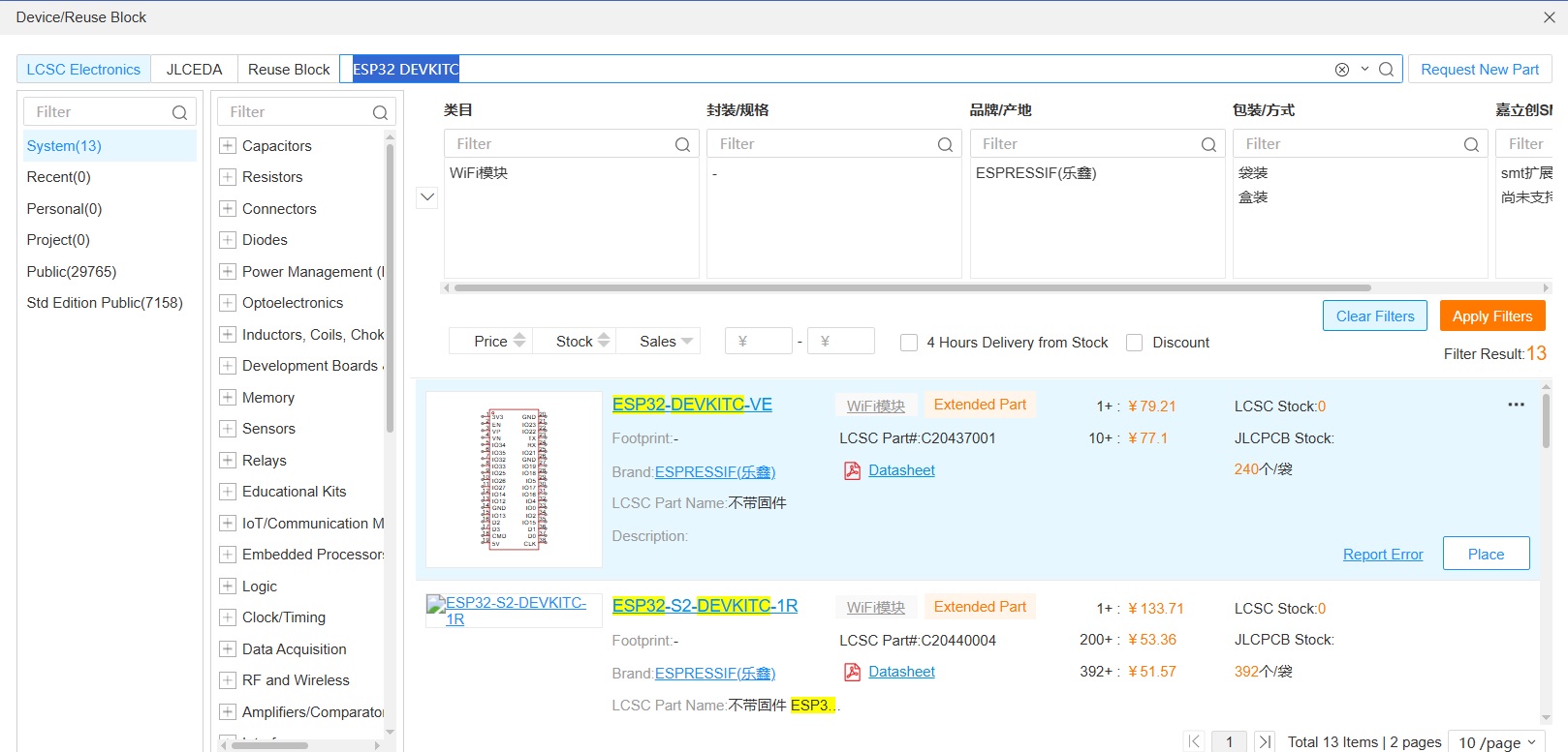
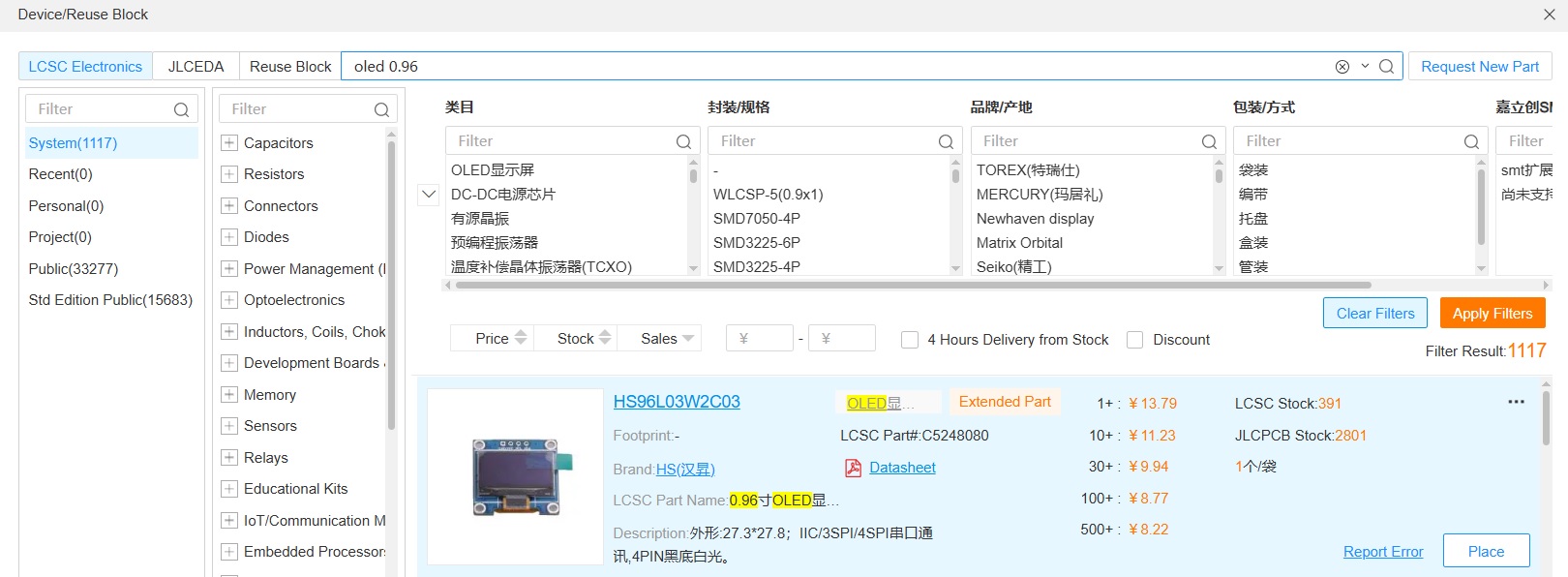
I use "Place -> Device" to select components from the library.
- Select ESP32 Dev Kit (38pin)
- Select OLED
- Select LED
- Select Resistor
- Select 3p pin header
- Select Button
- After select components, I assembly the component according above Componet list:
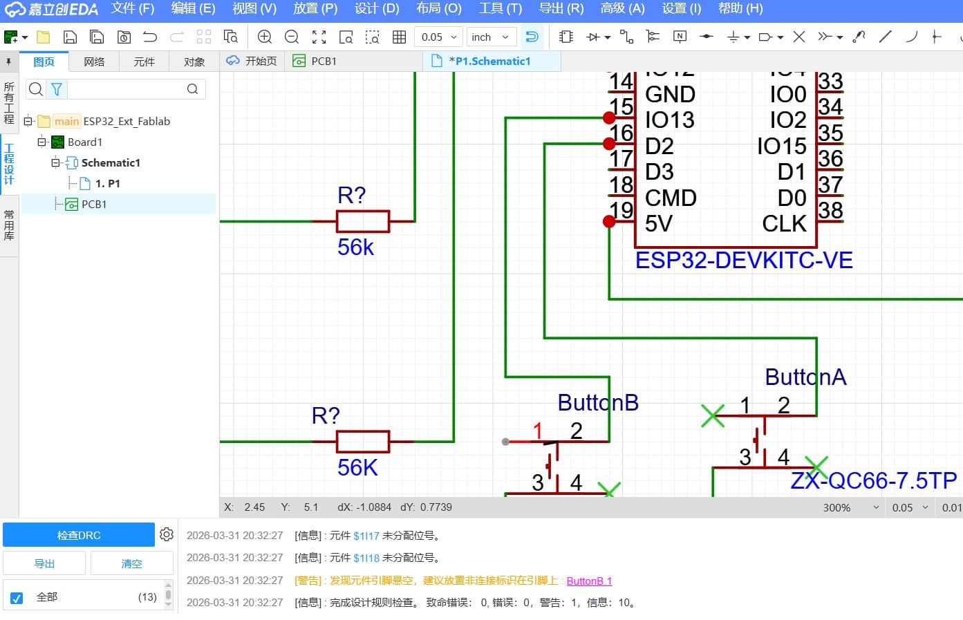
- I use "Design -> Check DRC" to ensure there were no errors in the schematic.
Such as the following, I meet an error about missing the "No Connect Flag".
I add the "No Connect Flag" to the Button component.
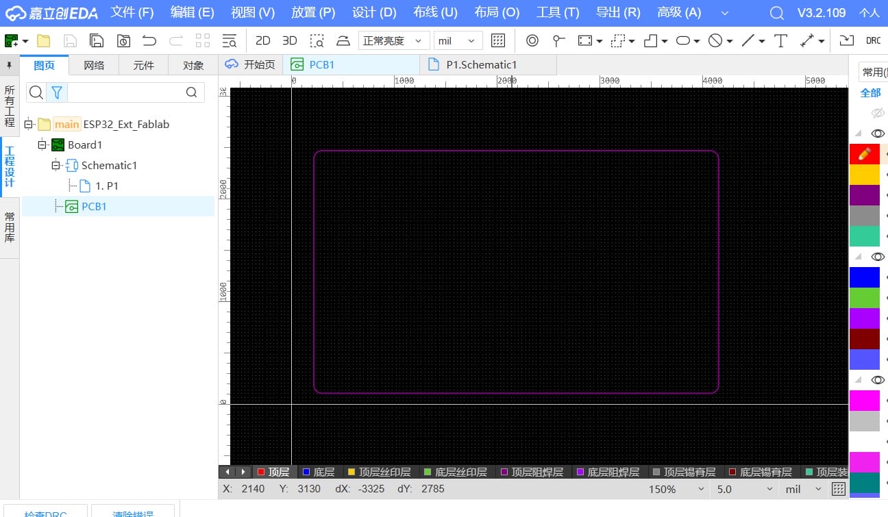
3.2.3 PCB Design
- I use "Place -> Board Outline -> Rectangle" to create a rectangular board outline.
- I use "Design -> import Changes from Schematic" to synchronize PCB layout automatic. I then manually arranged each component—dragging, dropping, and rotating them into optimal positions to ensure clean routing and a well-organized board.
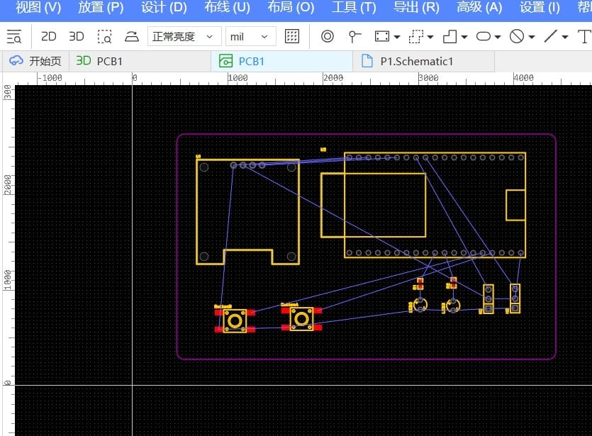
- I use "Route -> Auto Route... " to quickly complete the component routing, requiring only minor adjustments. I then reviewed and verified the routing on both the top and bottom layers. I added the logo and name.
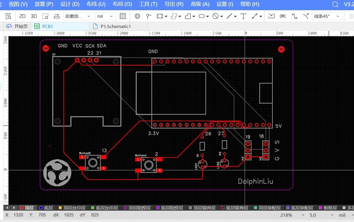
- I use "Place -> Copper Region -> Rectangle" to performed copper pouring.
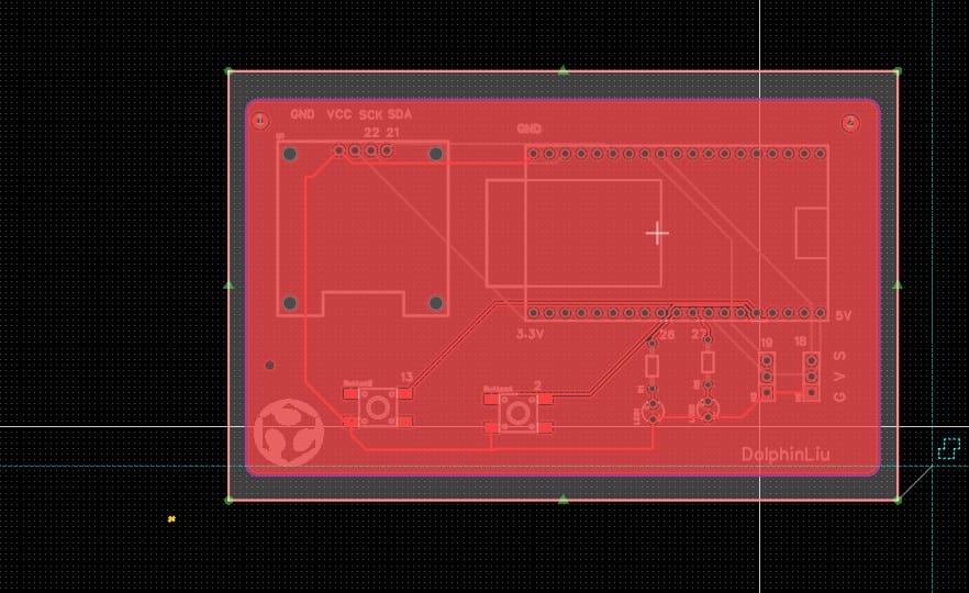
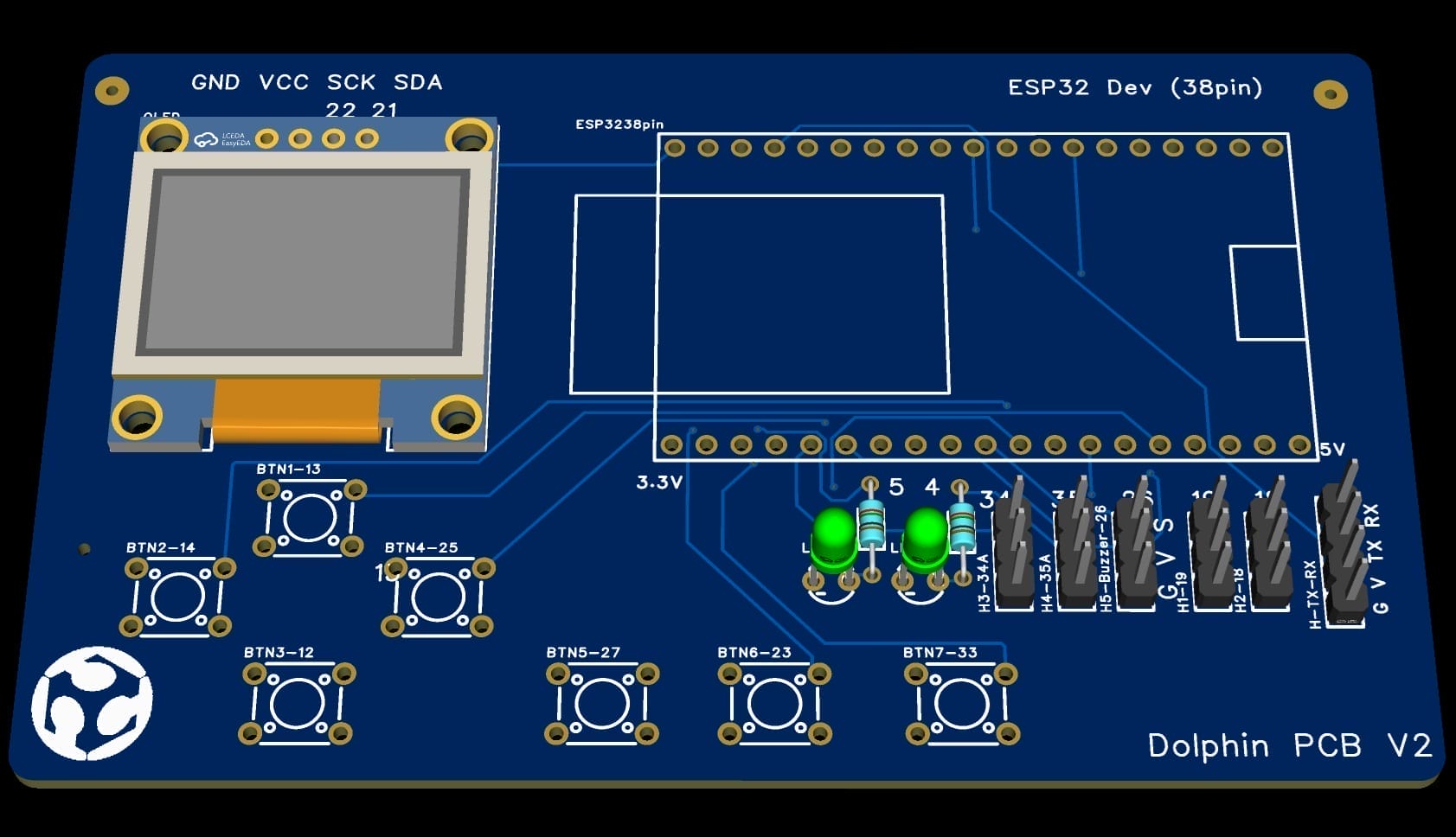
- I previewed the PCB in 3D to inspect the final design.
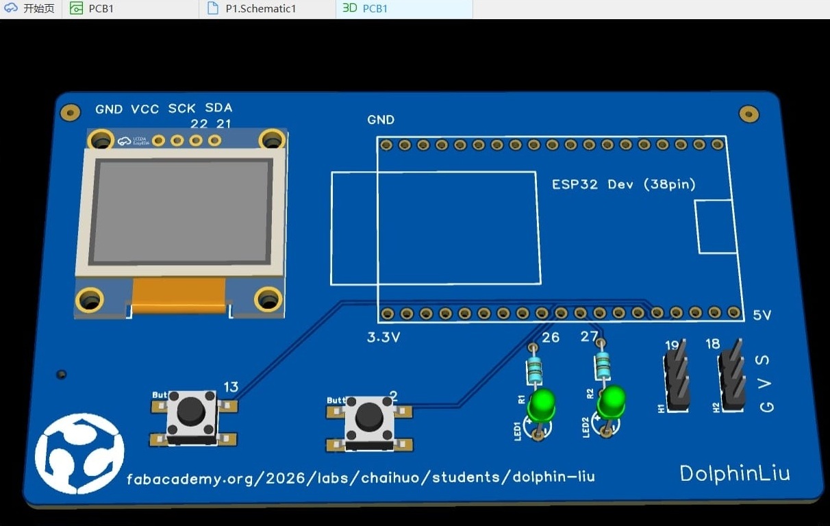
3.2.4 Preview
Here is the video of schematic,PCB and 3D preview :
3.3 PCB Manufacture
-
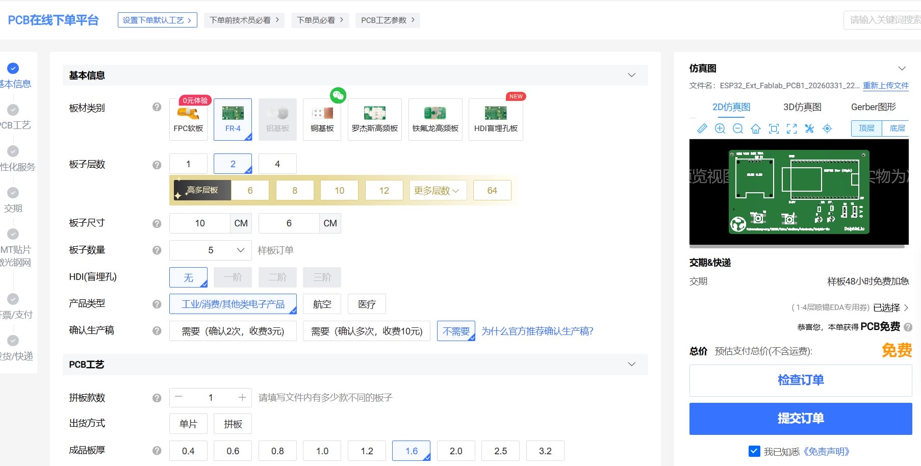
I exported the PCB design to Gerber files for manufacturing.
-
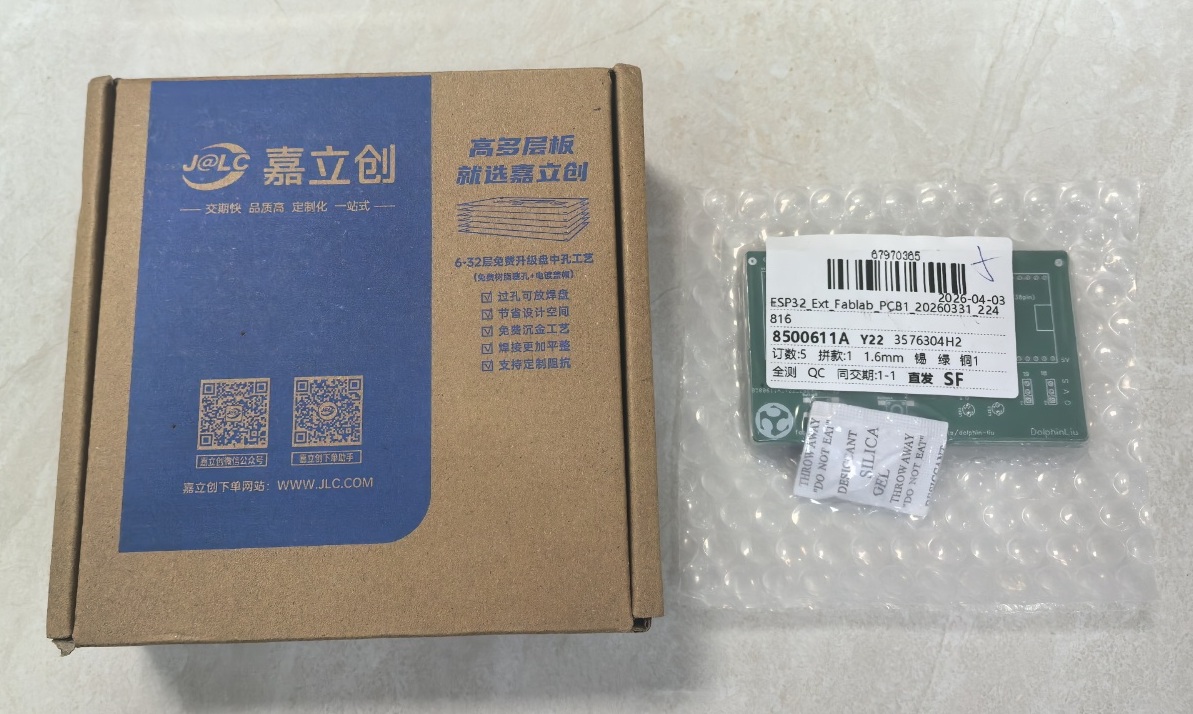
I order the PCB from JLCPCB.
-
After few days, I received the PCB box.
- The PCB is exactly what I expected
3.4 Resource
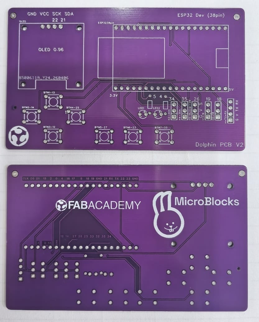
4.5 PCB V2
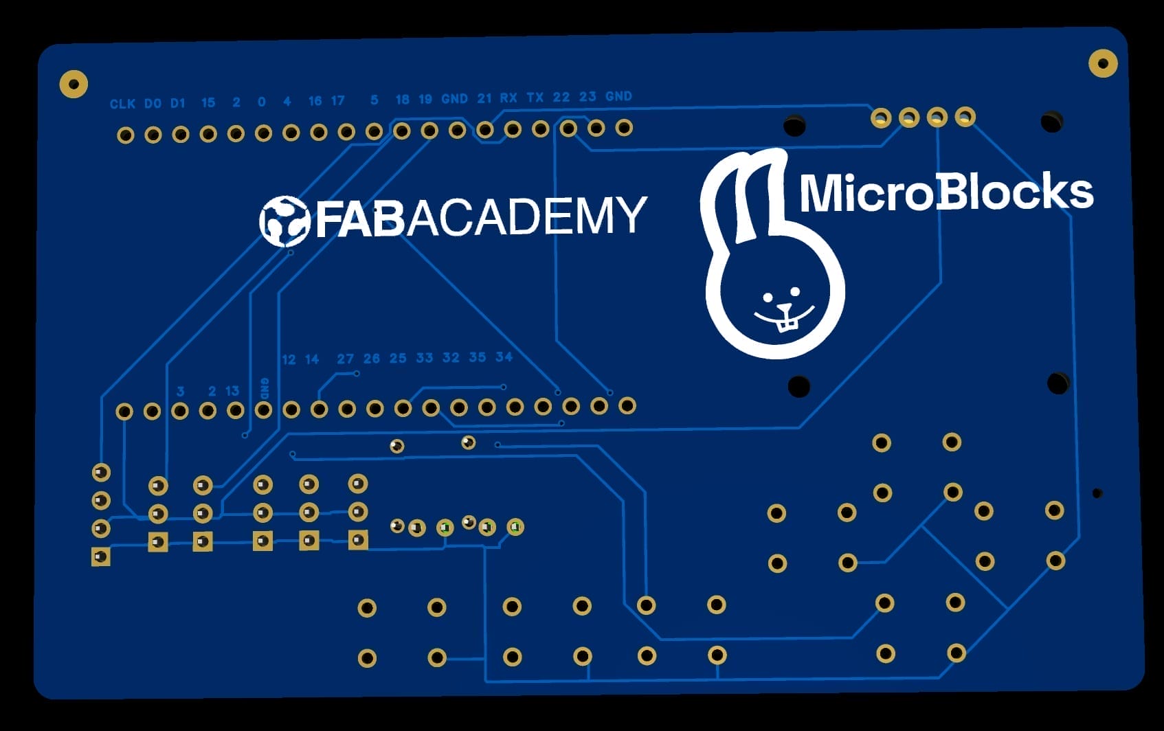
When I do assignment week09,week10, I find the PCB is not very good, I try to make a new PCB.
Here is the 3D preview of PCB V2.
 |  |
|---|
After few days, I received the PCB V2 from JLC PCB.