3. Electronic Design
3.1. PCB Design V1
I had design a PCB at week06 assignment. But I find some problems with the design.
3.1.1 Problems
Key Pin Conflicts & Lessons Learned
- GPIO2: Strapping Pin Conflict (Button)
-
Issue: The button connected to GPIO2 failed to respond or caused boot failures.
-
Reason: GPIO2 is a strapping pin that controls the ESP32 boot mode. It must be LOW during power-up to boot from Flash. If a button circuit pulls this pin HIGH at startup, the system may fail to enter the correct operating mode.
-
Lesson: Avoid using strapping pins (GPIO 0, 2, 5, 12, 15) for critical input components like buttons.
- GPIO18/19: Missing ADC Support (Potentiometer)
-
Issue: The rotary potentiometer failed to provide data when connected to GPIO18 or GPIO19.
-
Reason: These pins are digital-only and do not support ADC (Analog-to-Digital Conversion). Potentiometers require ADC pins to read varying voltage levels.
-
Lesson: Always verify the ESP32 Pinout to ensure analog sensors are connected to ADC-capable pins (preferably ADC1 to avoid conflicts with Wi-Fi).
3.2. PCB Design V2
3.2.1 Optimized Pin Assignments for ESP32
I would like to Optimized Pin Assignments for ESP32 in PCB Design V2. As my final project requires a wireless controller, I would like to add more button ,and pin header in PCB Design V2.
I search from google gemini ,and get some useful optimized suggestions.
To avoid boot conflicts (Strapping Pins) and ensure compatibility with Wi-Fi and analog sensors, use the following layout:
-
- 6 Digital Buttons (Input) Recommended Pins: GPIO 13, 14, 25, 32, 33 (and GPIO 23 if 27 is used for LED).
Reason: These are non-strapping pins. Using them ensures the ESP32 boots into Flash mode correctly every time, regardless of whether a button is pressed during startup.
-
- 2 Analog Inputs (Potentiometers) Recommended Pins: GPIO 34, 35
Reason: These belong to ADC1, which remains functional even when Wi-Fi is active (unlike ADC2). Note: These pins are Input-Only and lack internal pull-up/down resistors, making them ideal for voltage-divided analog signals like potentiometers.
-
- 2 Digital I/O (Retained from V1) Pins: GPIO 18, 19
Reason: Standard digital pins. They are reliable for general I/O and can also serve as the SPI interface (SCK/MISO) if needed later.
-
- 2 Onboard LEDs (Fixing GPIO 26 Issue) LED 1: GPIO 4 (Moving from 27 to free it up for buttons).
LED 2: GPIO 5 (Replacing the problematic 26).
3.2.2 Optimized Pin Assignments for ESP32
Here is ESP32 PCB V2 optimized pin assignment plan:
| Function Category | Quantity | Recommended GPIO | Description / Notes |
|---|---|---|---|
| Digital Buttons | 6 | 13, 14, 12, 27, 25, 23 | Avoids GPIO 0/2 to ensure smooth boot-up without strapping conflicts. |
| Analog Input (ADC) | 2 | 34, 35 | Dedicated to potentiometers. Use ADC1 (won't conflict with Wi-Fi). |
| General Digital I/O | 2 | 18, 19 | Retained from V1. Supports PWM, Digital Input, and Output. |
| Onboard LEDs | 2 | 4, 5 | Replaces the problematic GPIO 26 to ensure reliable lighting. |
| I2C (OLED Display) | 2 | 21 (SDA), 22 (SCL) | Standard I2C pins for maximum library compatibility. |
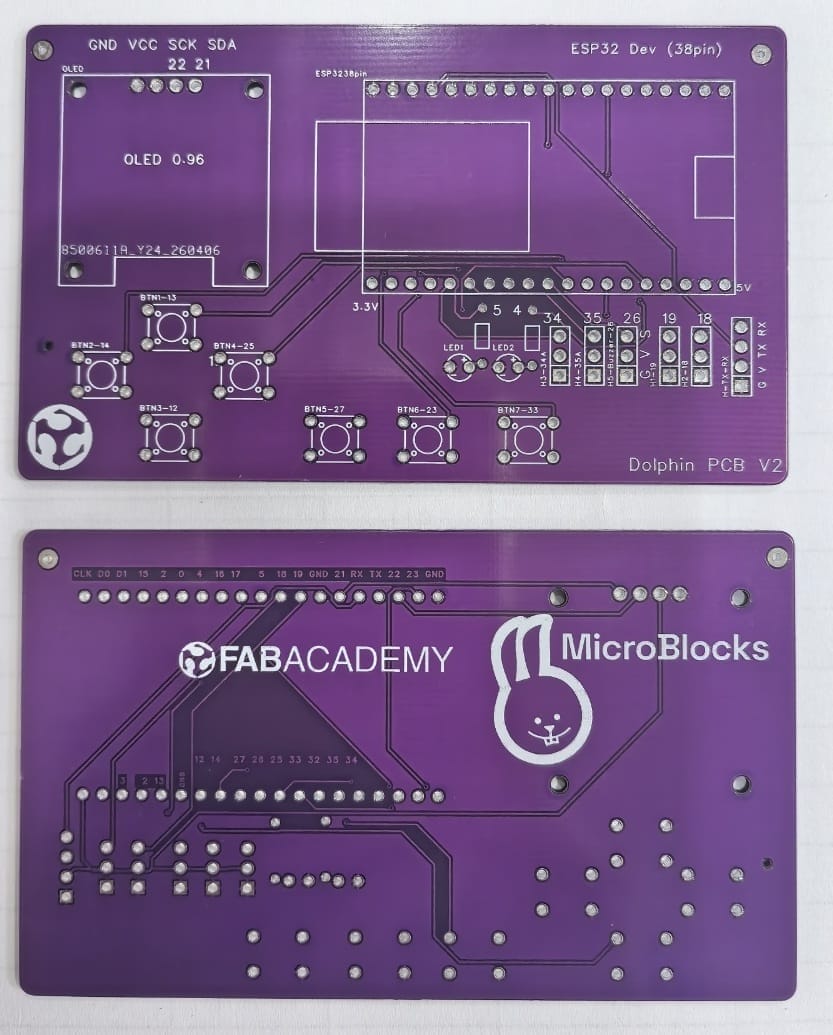
3.3. PCB Design V2 Design
3.3.1 Update Schematic
I open my V1 PCB design in JLCEDA, and update it.
I update the schematic ,add 4button , two 3pin headers, and one 4pin header.
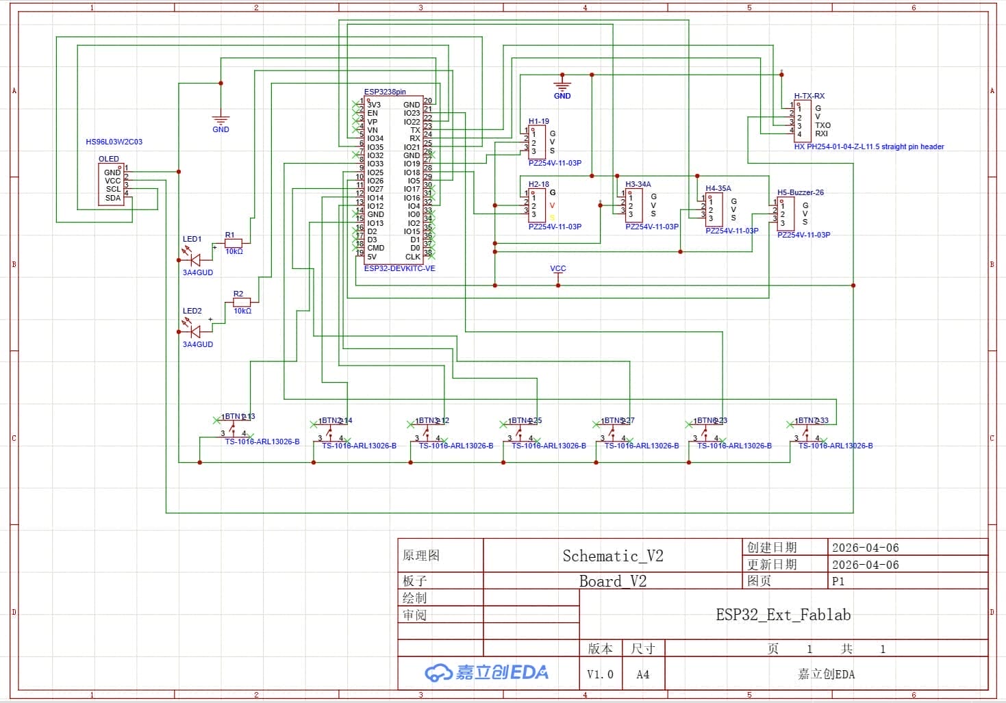
After I finished the Schematic, I select auto update to PCB design.
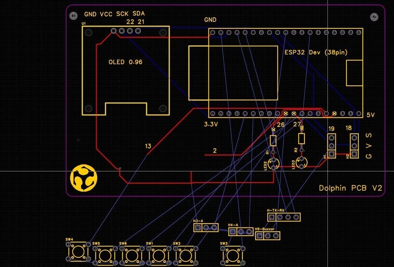
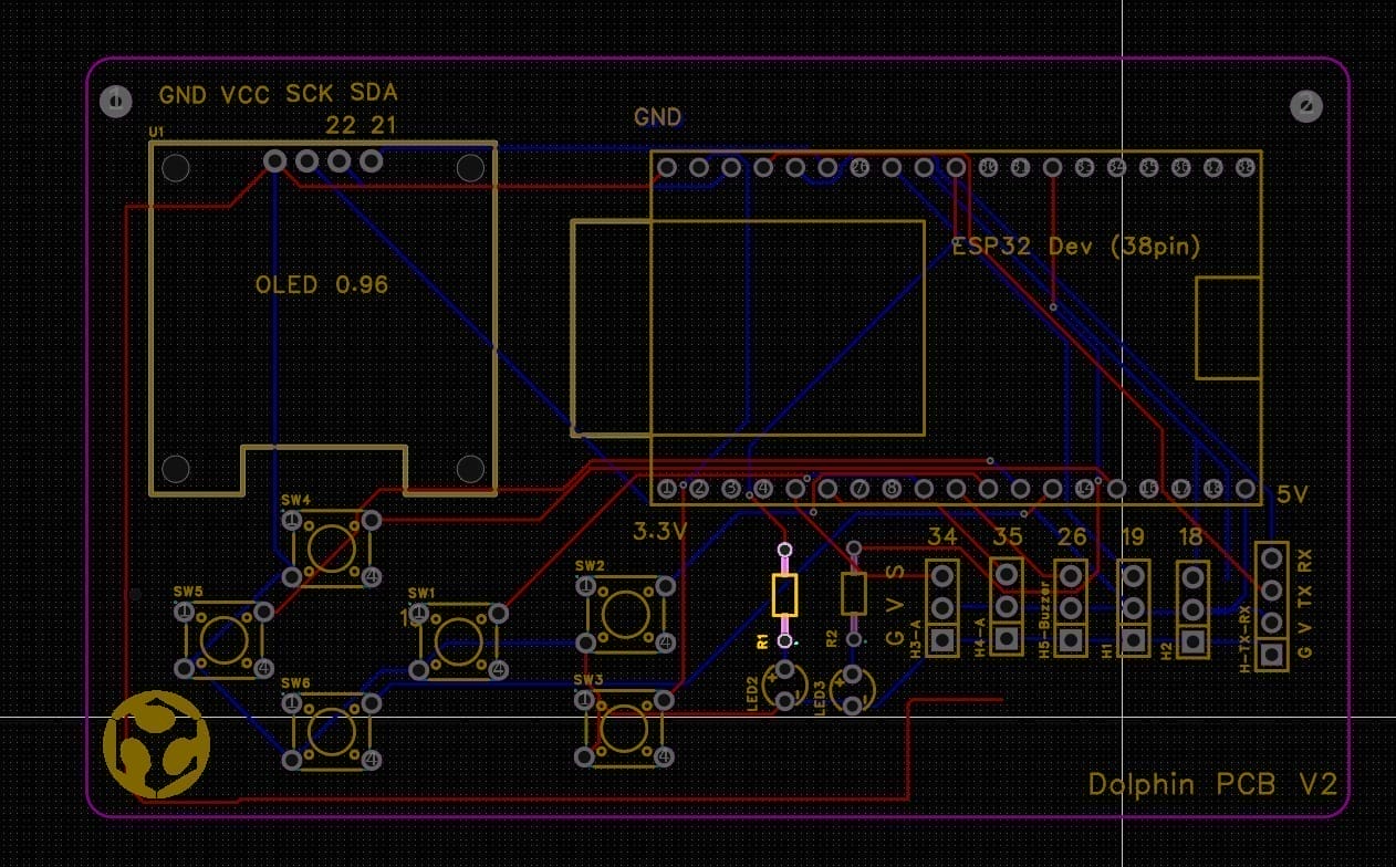
3.3.2 Update PCB Design
I move the button, pin header to the right side.
 |  |
|---|
I select auto routing ,and make some adjustments.
I meet some connection error. I adjust the connection and make some adjustments.
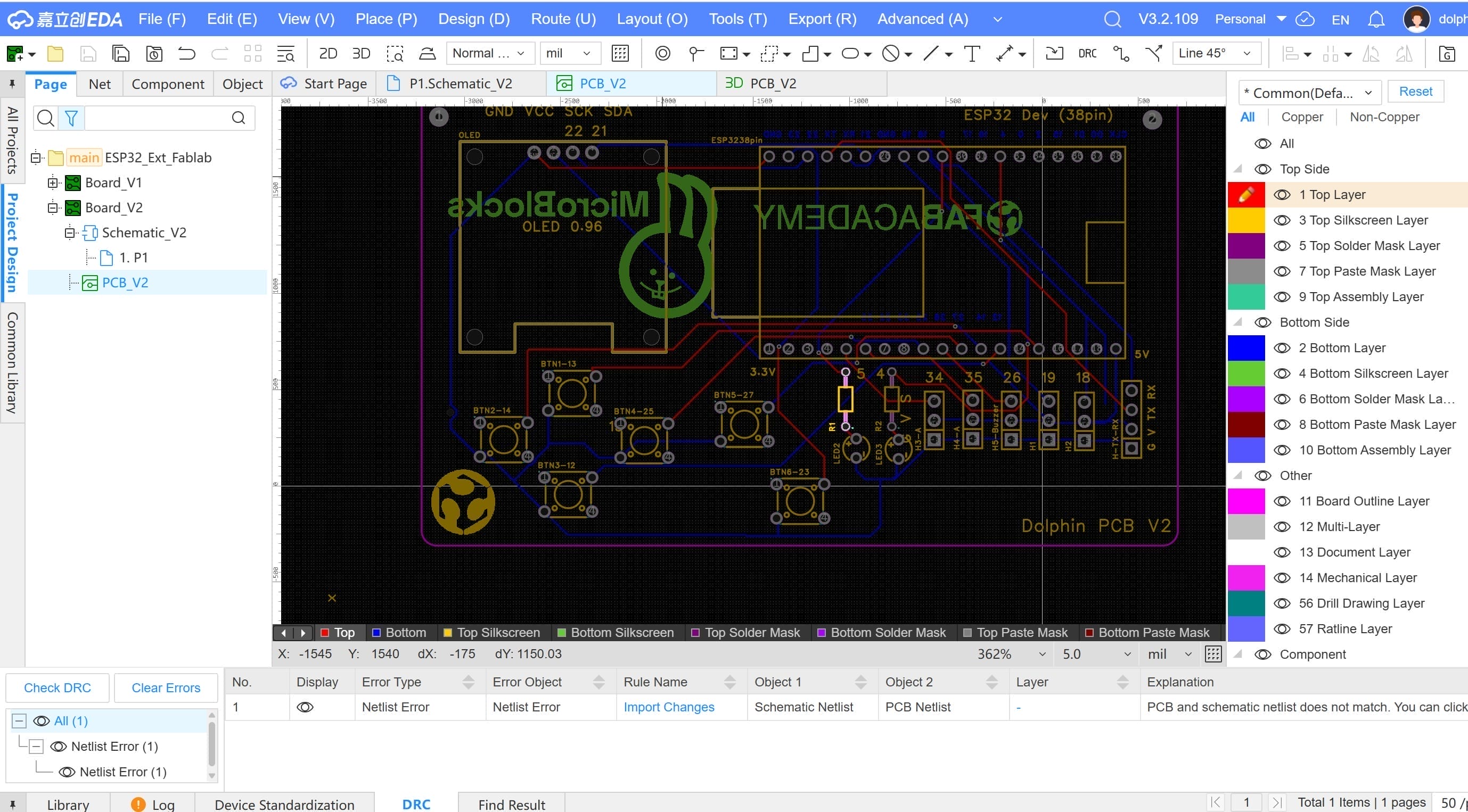
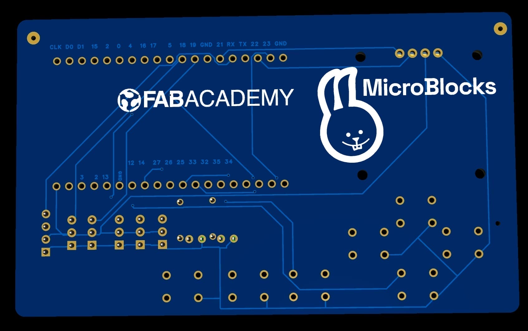
I finished the PCB design.
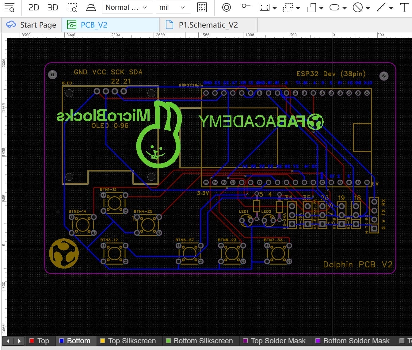
I have performed copper pouring on both the top layer and the bottom layer.
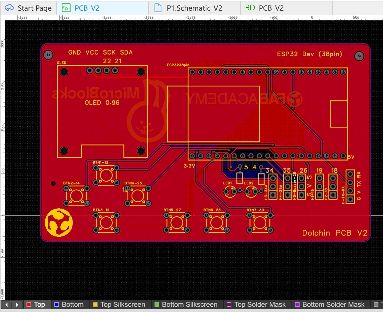
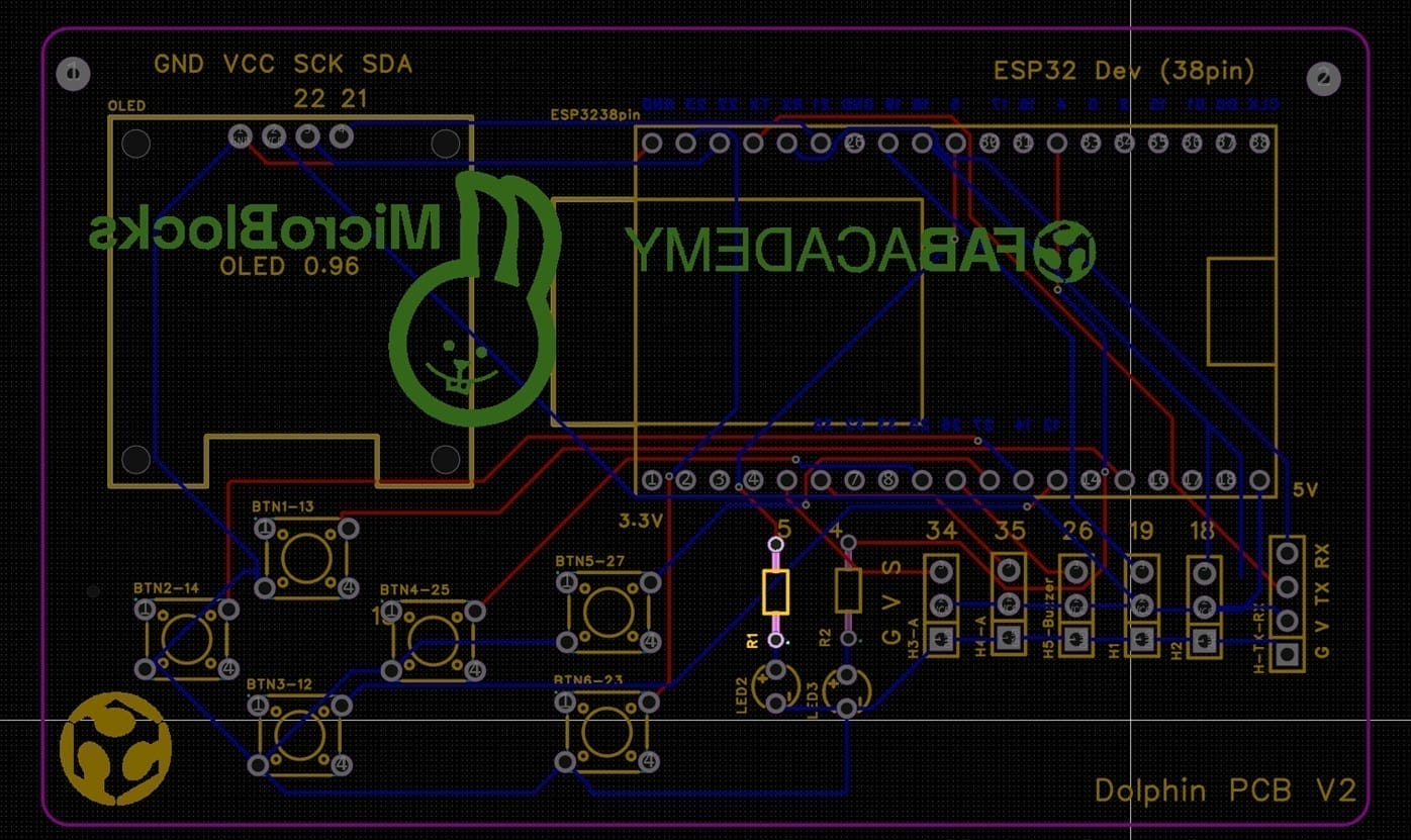
3.3.3 3D View
Finaly,I can review the PCB 3D view.
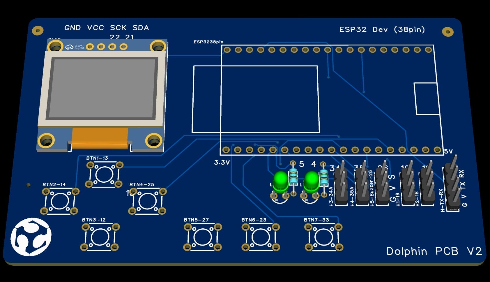 |  |
|---|
3.4 PCB V2 Testing
-
I submitted the PCB to JLC online.
-
After few days ,I receive the PCB from JLC PCB.
- I soldered the PCB.
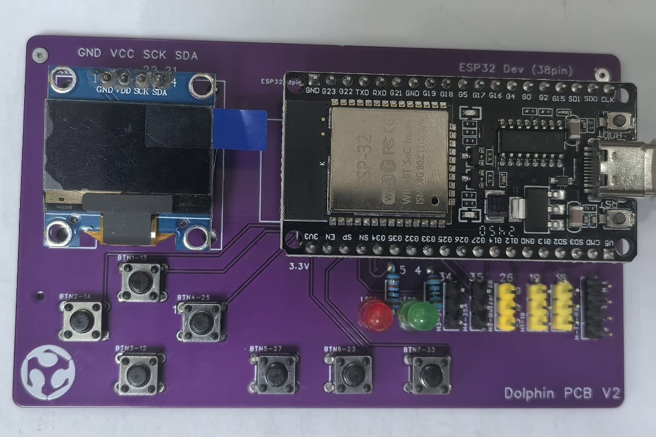
- Here is the video of testing.