Assignment
Group assignment:
- Characterize the design rules for your in-house PCB production process: document feeds, speeds, plunge rate, depth of cut (traces and outline) and tooling..
- Document the workflow for sending a PCB to a boardhouse.
- Document your work on the group page and reflect what you learned on your individual page.
Individual assignments:
- Make and test a microcontroller development board that you designed.
Group Assigment
we made a design rules for our in-house pcb Production and did some test.
Click on this button to get it to our Group Assignment Page
Individual Assignment
heroshot


Exporting to Gerber file
1. Previously on electronic Design, i have done the design in it and open the PCB deisgn of it.
2. Go to File -> plot and click on it.
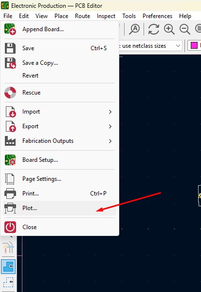
3. click on the layers that you may need, in my case i need F.cu and edge cuts layers on it and click on teh output directory and change the directory on it.
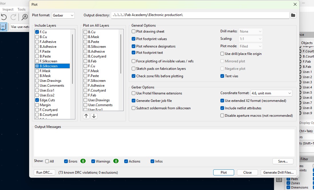
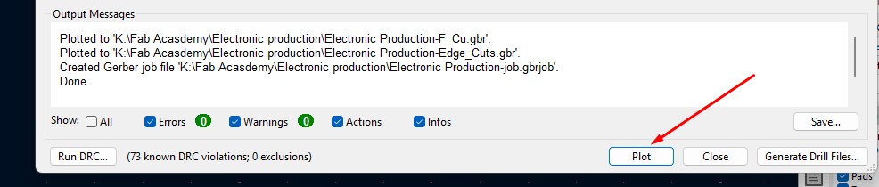
4. click on the "Plot" button and the file has been generated.
Introduction to FlatCAM
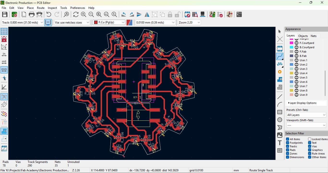
FlatCAM is an open-source software tool used primarily for preparing PCB (Printed Circuit Board) designs for CNC milling. It takes Gerber files (generated by PCB design tools like KiCAD, Eagle, or Altium) and converts them into G-code, which can be used by a CNC machine to mill the PCB..

Installation of FlatCAM
1. Go to Google to Search "FlatCAM" to get the FlatCAM official website (www.flatcam.org) , Click on it .

2. in that Flatcam website -> sa you may see over there you may click download.

3. if you click over there and there will be lot of os version to download in there click it on Windows(as i having windows to use it).

4. in that you may see many version and in that download latest one in it.

Here is the link button below:
to download the FlatCAM version
Or you can download manually:
Click here to download KiCAD
Opening the software
After Opening the FlatCAM, a Window will pop up that is Main Windowand you are gonna work on it.

Converting Gerber files to G-CODE
1. This is the main window. you should use that in well about it.

2. click -> open -> open Gerber.

3. Click all the contents and "open" it.

4. as you seen over here, the contents will be displayed in it.

5. move all the file to the origin axis in it.

6. right click the file and -> move then move it.

7. Move all the contents in the Origin.

8. Click the F-CU copper gerber file and double click it.

9. In that There are many option to do in that We ahve to Click "Isolation Routing" that is this will isolate the route taht we need to do and it should be done for tracks in PCB. click on it.

10. In that there will be tools table in which we have to do is give bit diameter in it. after giving diameter in it just need to give the passes (how many layers of cut you may required) for mine i gave around 4and click "Generate Geometry"

11. After that you can clearly see that in which the diagram or your design is changed and having many layers.

12. In that change the V-tip size that is on 30 degree and overly mentioned that and spindle speed is should be around 10000 and click on "Generate CNCJob object".

13. as you have seen over there, everything has been done and you just need to save the g-code that has been generated that is by clicking "Save CNC code"

14. A small wiondow will pop up navigate where you wanna save, then click "save" to save it..

15. after completion for F-Cu file that is track file . let's do it for the outline file aslo in there by Double-clicking on it.

16. A window will pop up same as for track routing instead of selecting Isolation routing click "Cutout tool" in it to outer-cut the File.

17. another window will come that will be different from previous windows in that you have to generate the geomentry by giving tool diameter - that is 2.0 (its in our lab file) and give cut z to -1.8 and click "Generate Geometry" into it.

18. if you go to main window you may visit a new geometry in it. double click It .

19. it may look like similar window click on it and customize the value as you needed as in spindle speed that is 10000 and click "Generate CNCJob Object" that will create a structure..

20. you can clearly see and there will be a option to save by clicking "Save CNC Code" to save it.

21. A small window will pop up and navigate the path and there will be to save the file and click it.

22. As you have seen over here there are two files that is the G-code been generated.
PCB Milling Machine
PCB milling involves mechanically removing material from a copper-clad board to create electrical isolation and form circuit patterns. Unlike traditional etching methods, which use chemical solutions to dissolve unwanted copper, milling uses precision-controlled milling bits to physically carve out the desired traces. The process is typically carried out using a Computer Numerical Control (CNC) milling machine, which is programmed to follow a specific design layout to guarantee accuracy and repeatability.
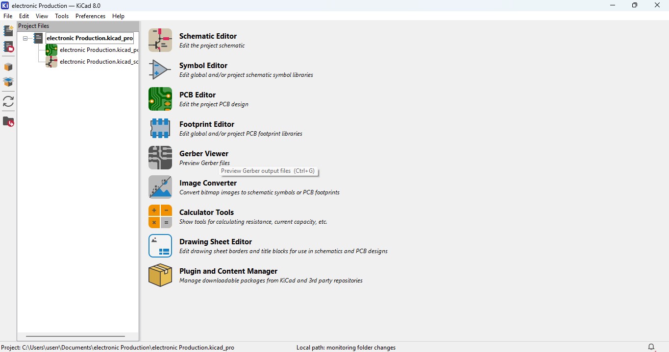
1. Open the Kicad and main Window will pop up and go to File -> New Project
2. Browse the location and name the Project in my case i have added "electronic Production"
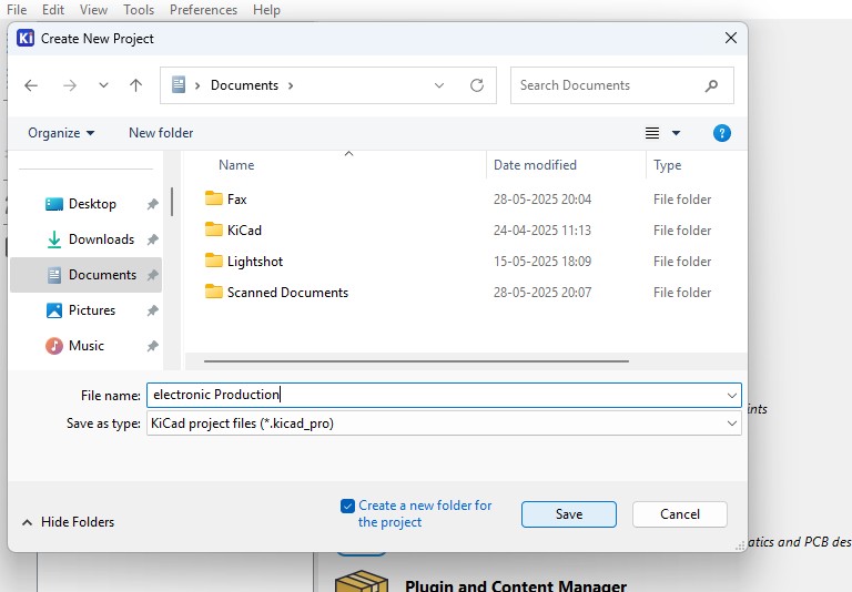
3. you may see the there are two files that is
- Schematic File (.sch)
- PCB Layout File (.kicad_pcb)
Idea generation of making Design
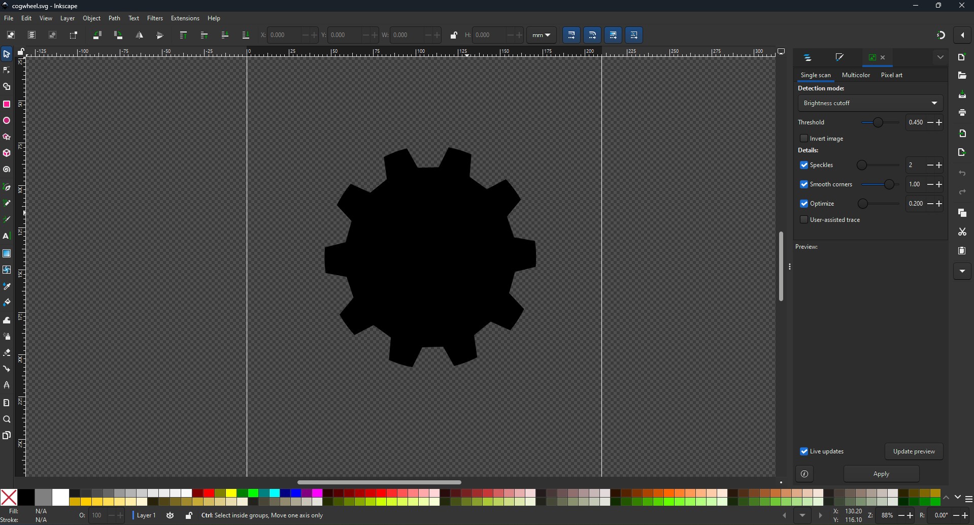
1. I though to make a design that is different from somethinga dn i need to be in circular so i searched for the many this i got an awesome idea to make a design that is CogWheel in it.

2. download a image and im gonna use Inkscape software to edit the design simailar to make it on.
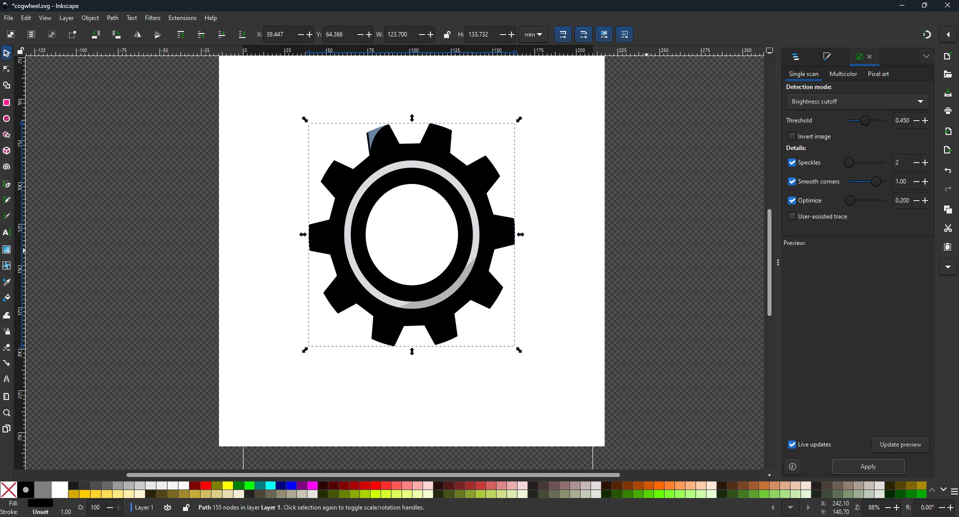
3. and this is what i made from it and downloaded as a SVG file so that i can move it as a outline on my board
Making Schematic for your circuit
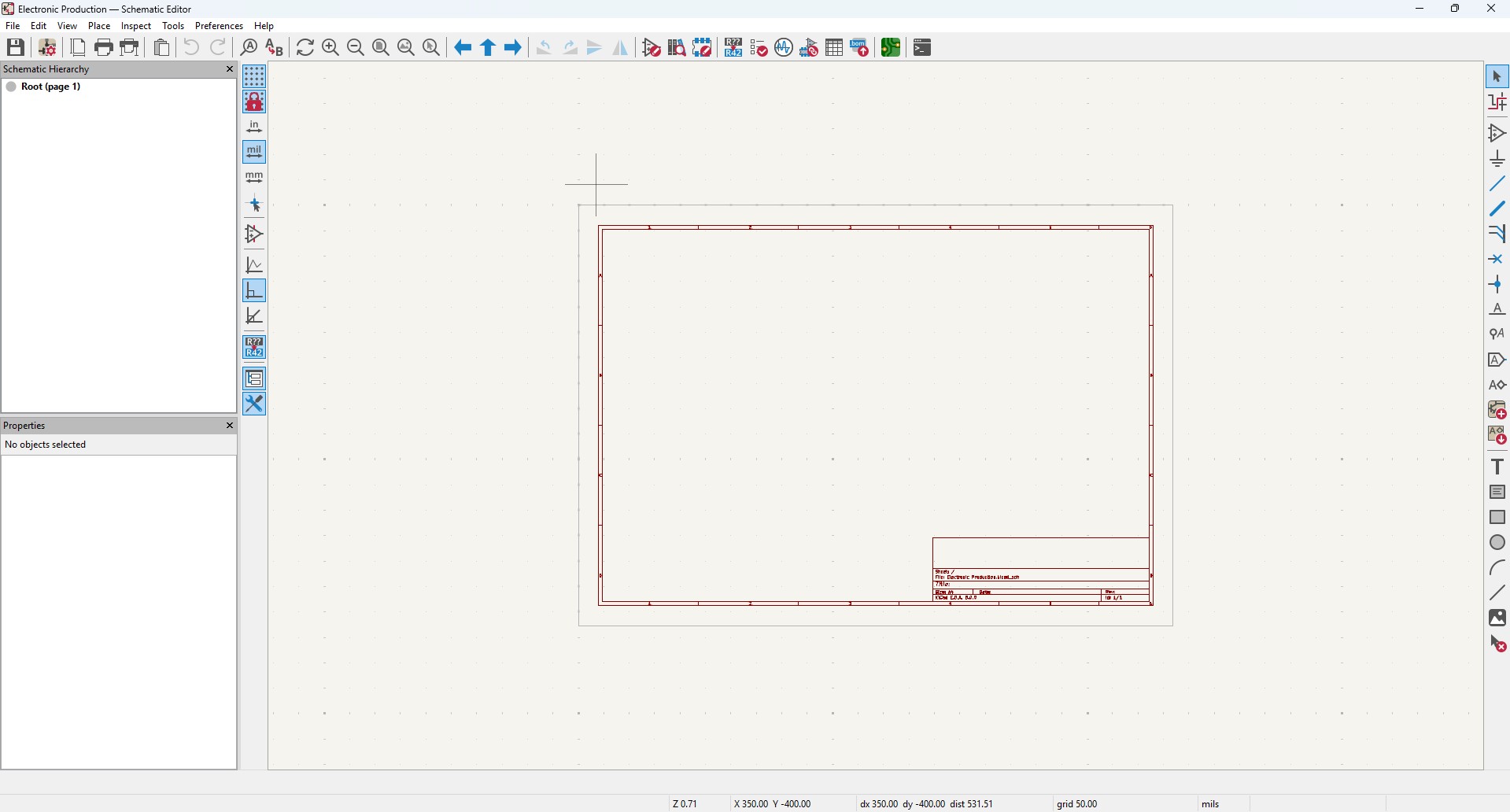
1. Open the Kicad and main Window will pop up abd click on the Schematic Editor
2. A new Window is pop up that is Schematic editor weher you make schematic diagrams for your circuit
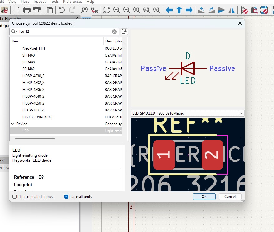
3. By clicking "A" or click on the 3 option on the right panel that is "add components" to add new components. a new window will pop up
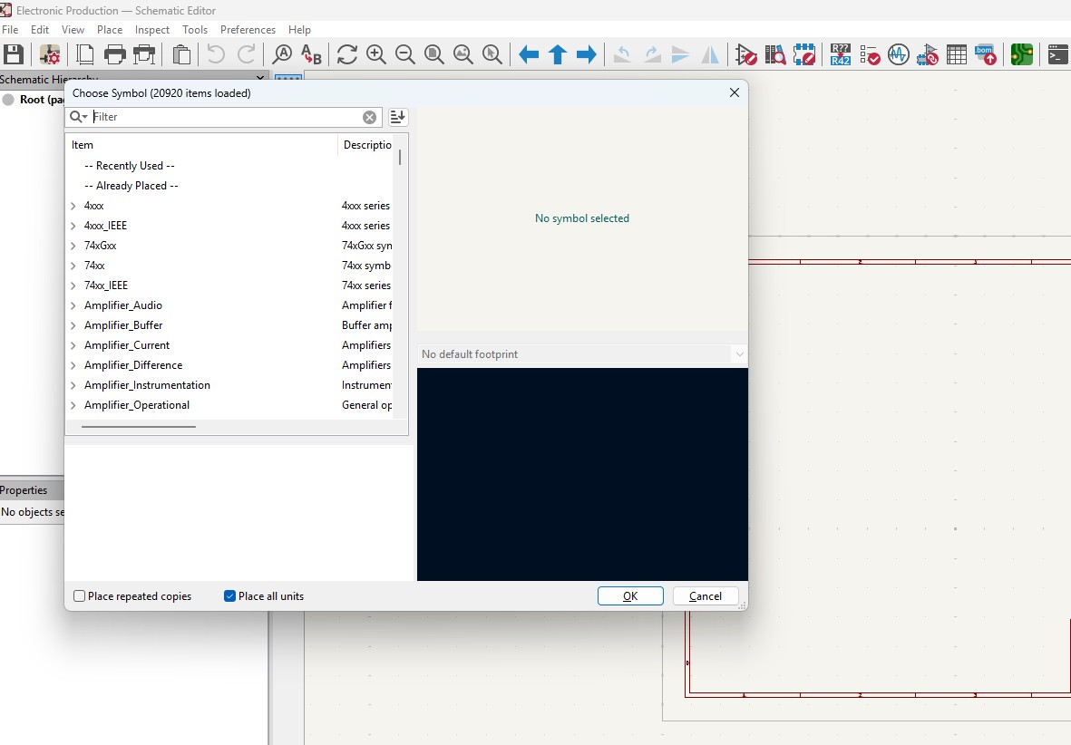
4. search of the components that you may required in it so in this assignment i wnat these components in it
Components required
- Seeed studio Xiao ESP32C3 module X 1
- SMD LED (1206) X 10
- SMD resistor 100 ohms (1206) X 10
- SMD resistor 0 ohms (1206) X 10
- KY - 004 Tactile switch X 1
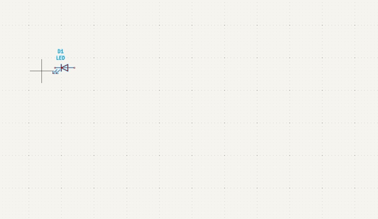
So im searching the component LED in it.
5. place the components in it
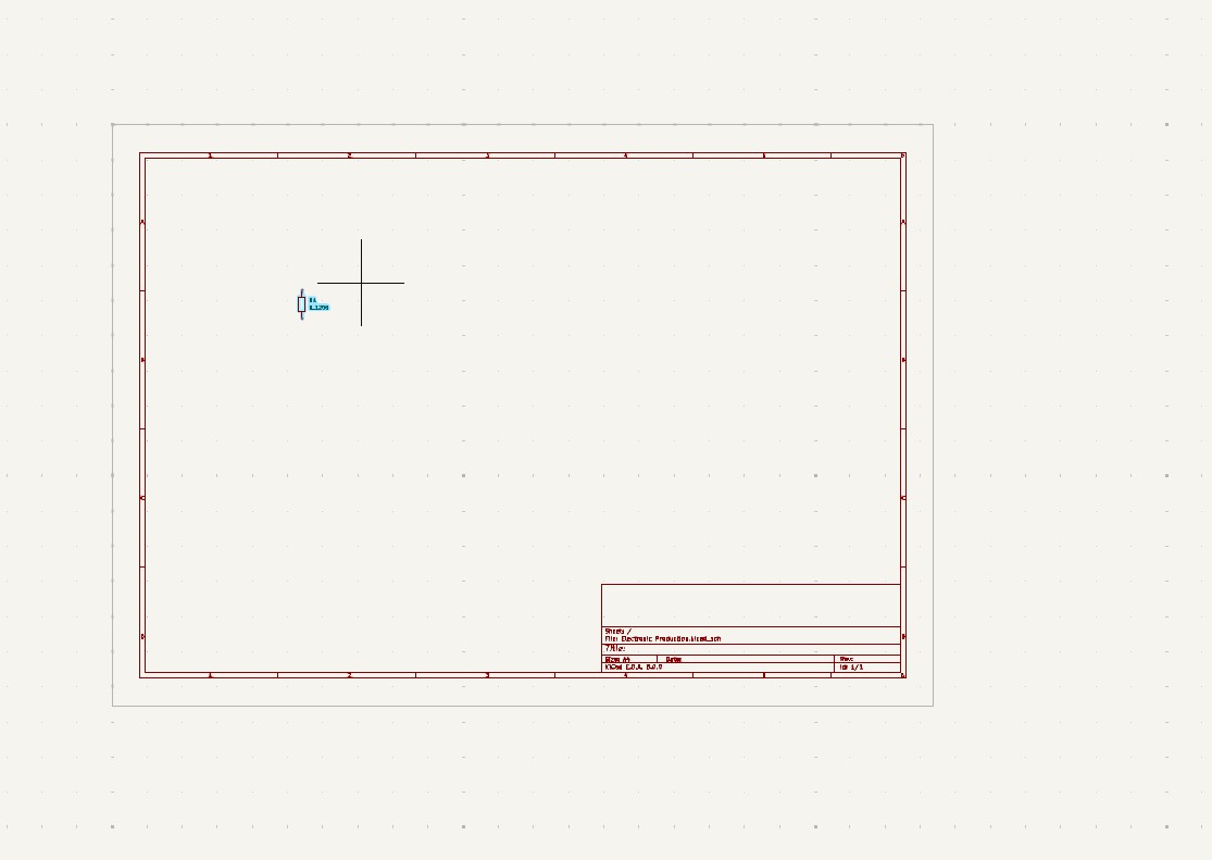
6. Duplicate the contents as per your needs.
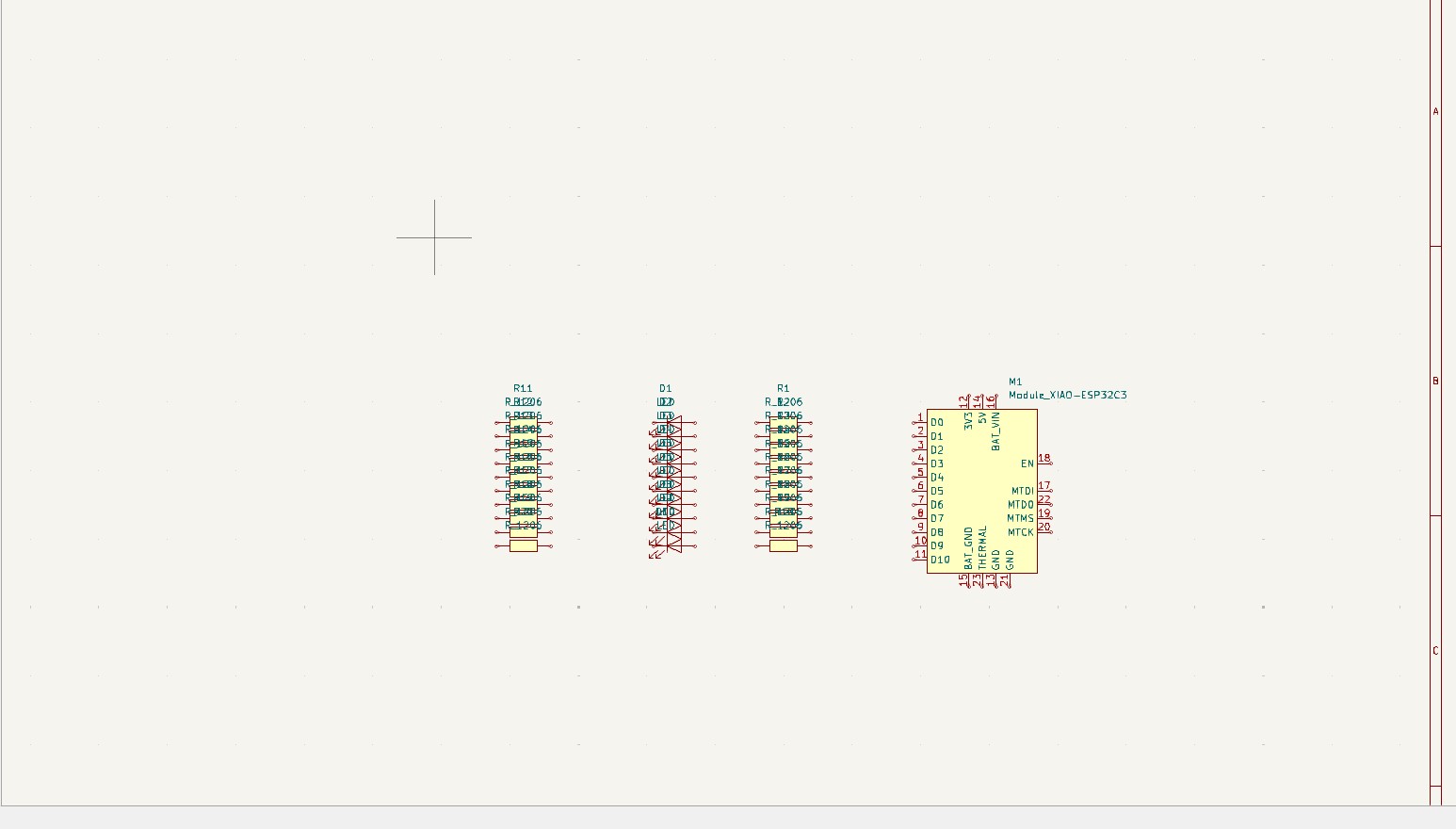
7. As you have seen that i have places all the components in it with its quantities
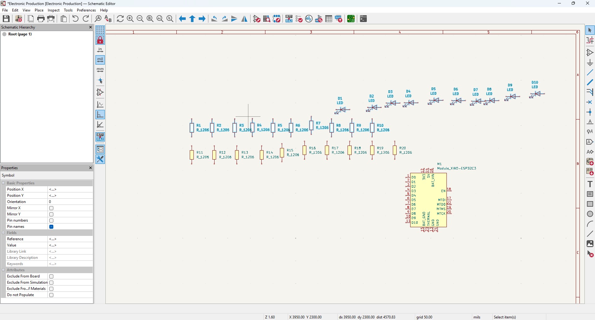
8. Arrange all the components as per the you convienent and i made it look like this in it
9. Give the Circuit Connection as per your need that is by clicking "w" or click on the 5 option on the right panel that is "wire" to give connections in it
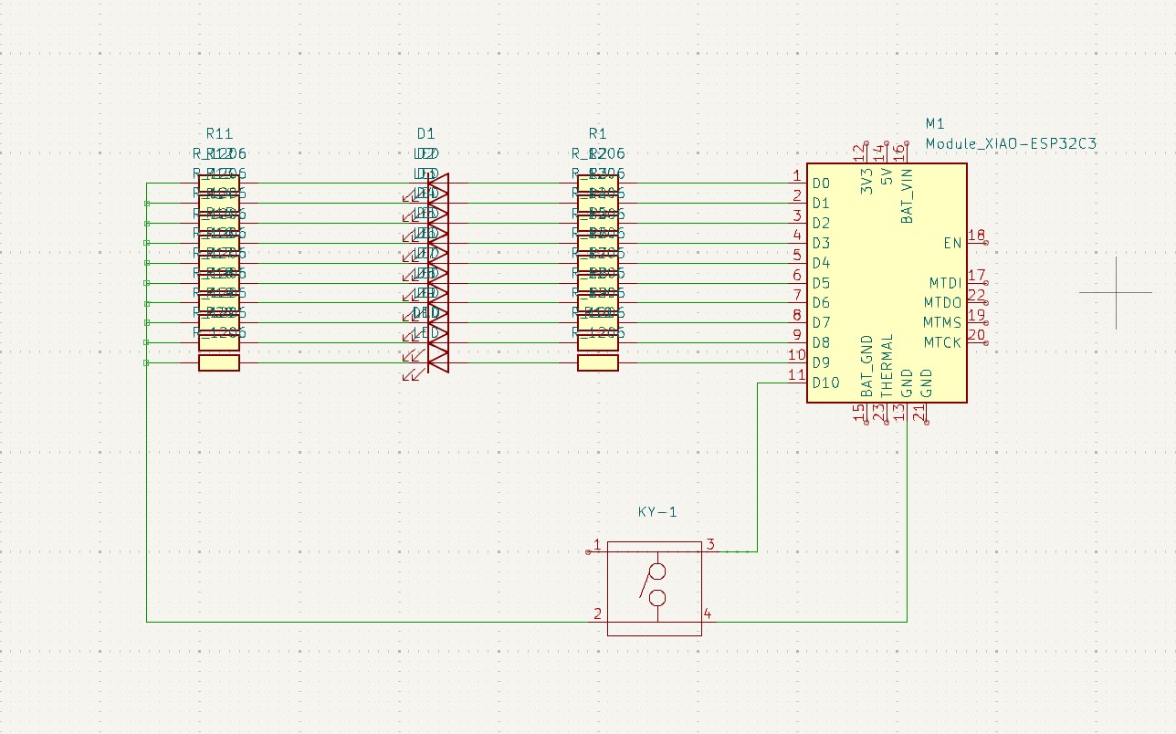
10. After all the connections are given, the remaining not connected pins are needed to connect this pins that is "no connection flags" that is avaialbe on 8th block which is in on right panel.
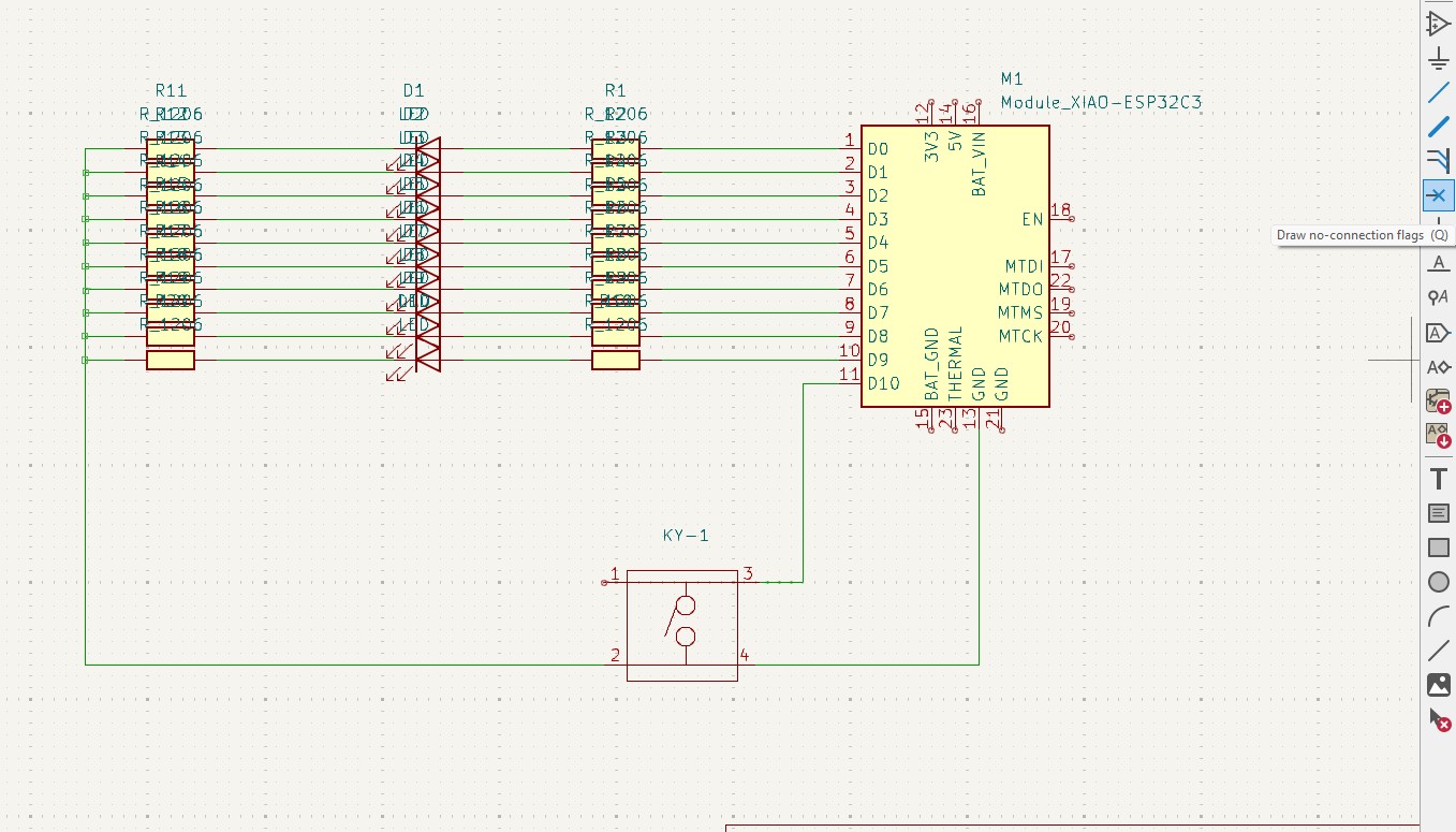
11. after connection all that flags you may see like this connection .
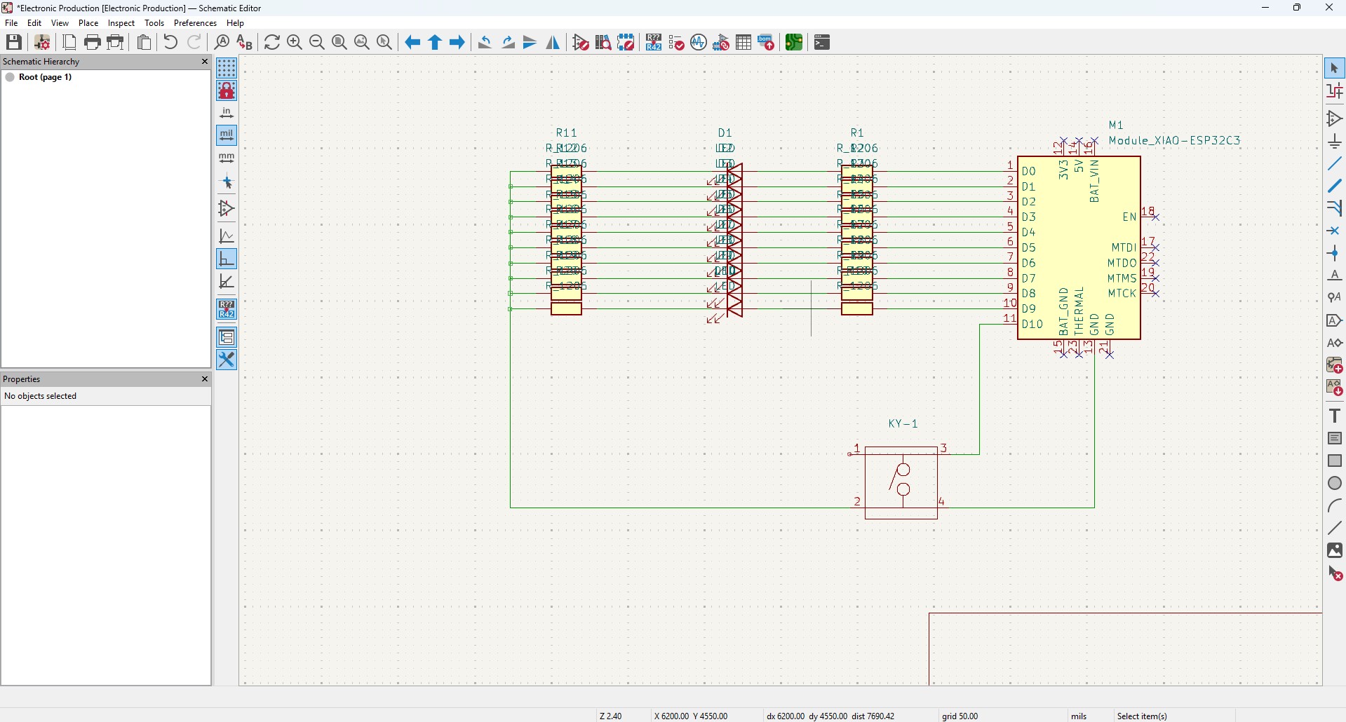
12. After all connection, go to Inspect -> Electrical Rules Checker. Click on it
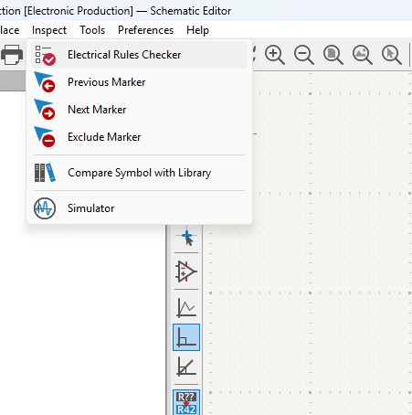
13. A new window will pop up and it is mainly used to check if there is any issue or not . so do that click on "Run ERC"
14. It may start to run checker and finds all the issue and error or warnings that are available in your circuit. so find all are correct are not.
15. After doing all the things, click on the "Open PCB in board editor" to import the design from schematic design to pcb design.
Making PCB design from the Schematic Diagram
1. Open the Kicad and main Window will pop up abd click on the PCB Editor
2. This Windows is used for the PCB design that you make in schematic design.

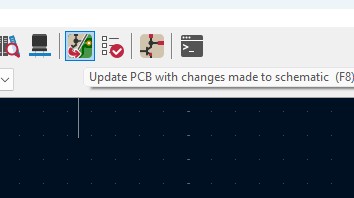
3. Over top, you make see the symbol like that, that is used to update the PCB with changes taht made in schematic. so click that.
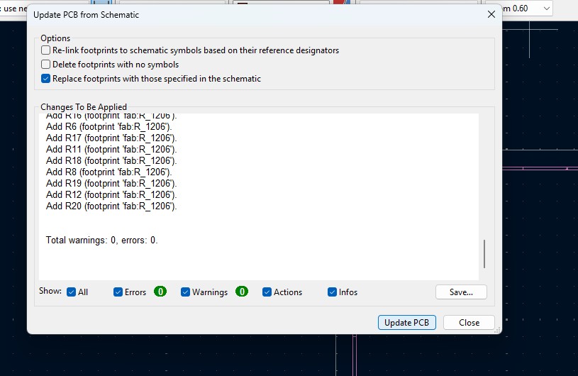
4. A new window will appear over that click on "Update PCB " button and all the components may list out over here click on it.
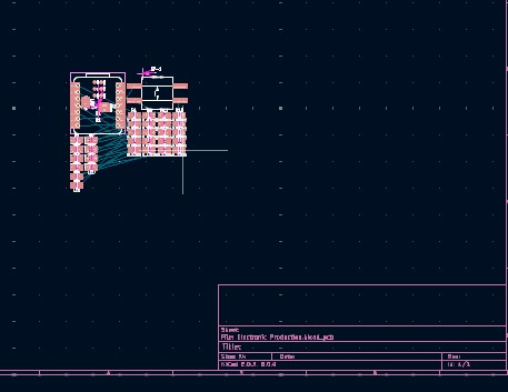
5. all the components are updated in the PCB editor and as you been seen over here.
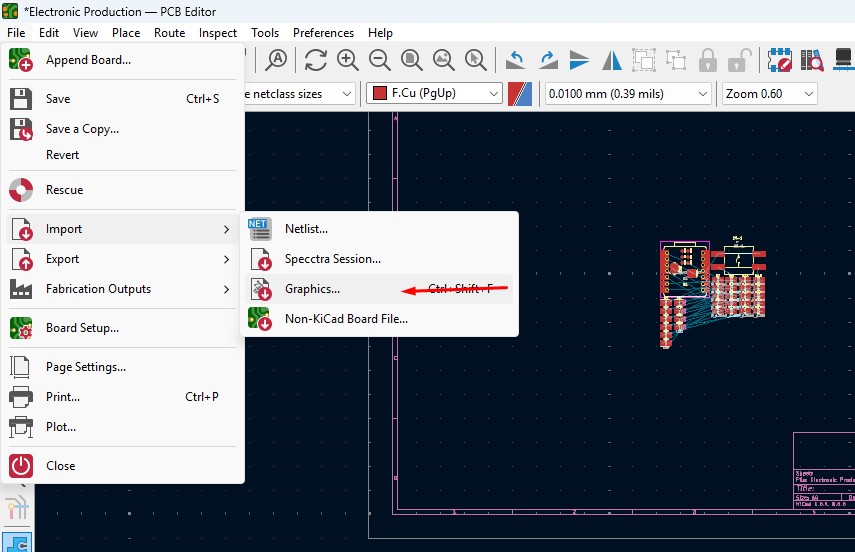
6. Click File -> Import -> Graphics and click it to import Outline of the board.
7. A New Window will pop up and over there will be a changable dropdown go o there and click that to "Edge.Cuts" and click on the folder button change the directory.
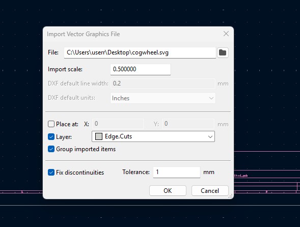
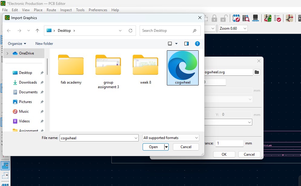
8. A new window will come over there navigate the directory to the file where the SVG file is located and clicked on it.
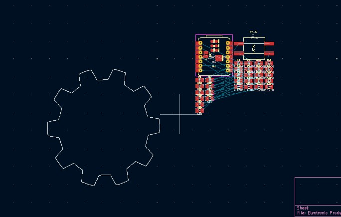
9. The Edge cut outline gets out over here (as i used Cog Wheel in it) place it on.
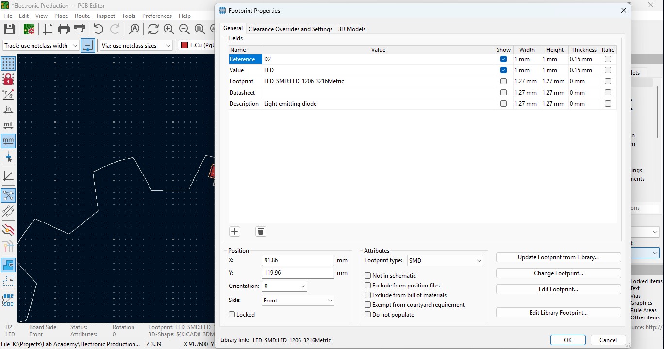
10. Click on the component and double click it and "Footprint Properties" window may appear on the orientation and change the degree to the convienent way so that adjust it on and place it.
11. Place all the Led components in the teeth of the outline as i did.
12. place all the resistor and do the same for it also as did for LED in it and rearrange it.
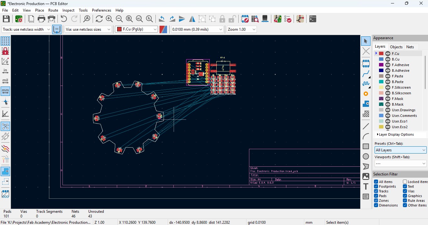
13. Over the right panel there are all things, click on the fourth block that is "Route Tracks" or click on "X" to start the routing.

14. Over the left upper panel and click on the "Track: use netclass width" and change that to "edit pre-defined sizes" and click it.
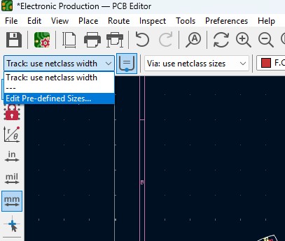
15. A new window will pop up and click on (+)icon on the Track Column "width" and click on it.
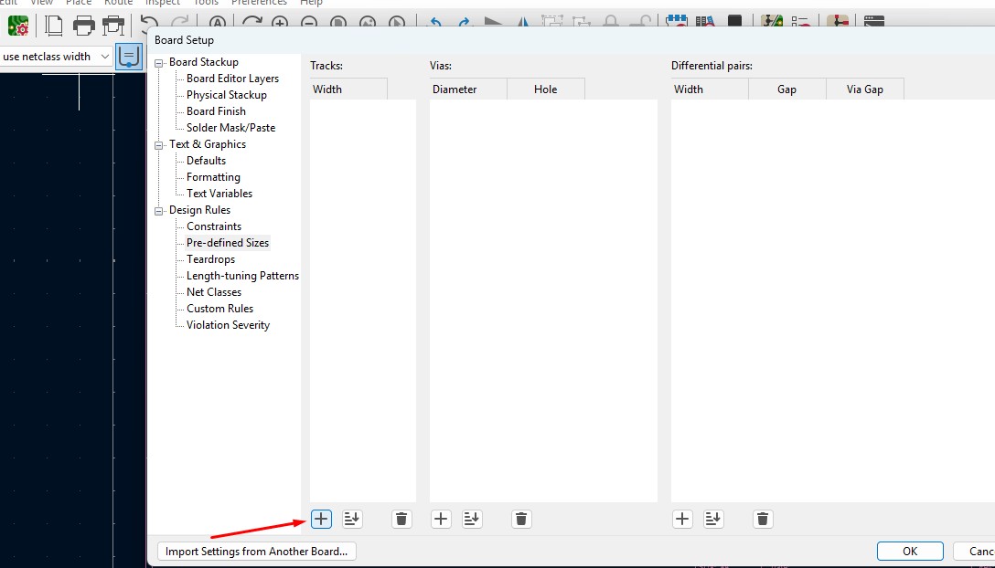
16. Change that to the your wish track size so for me i gave it to 0.8mm track width size. and click it
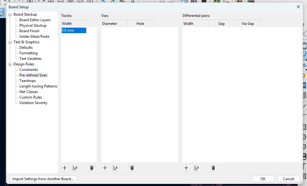
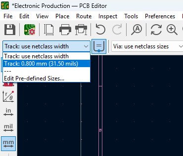
17. Now click on th esame track width in there you may see track 0.800mm width size in it. click it.
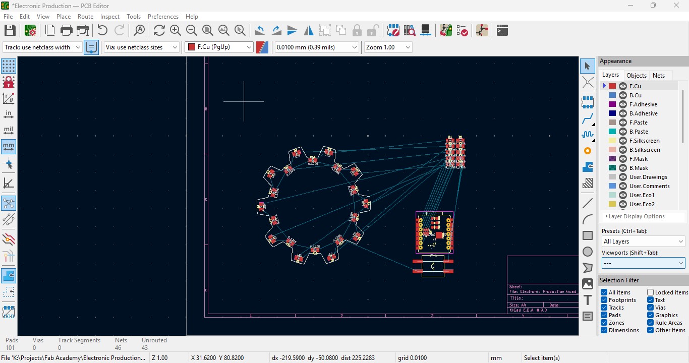
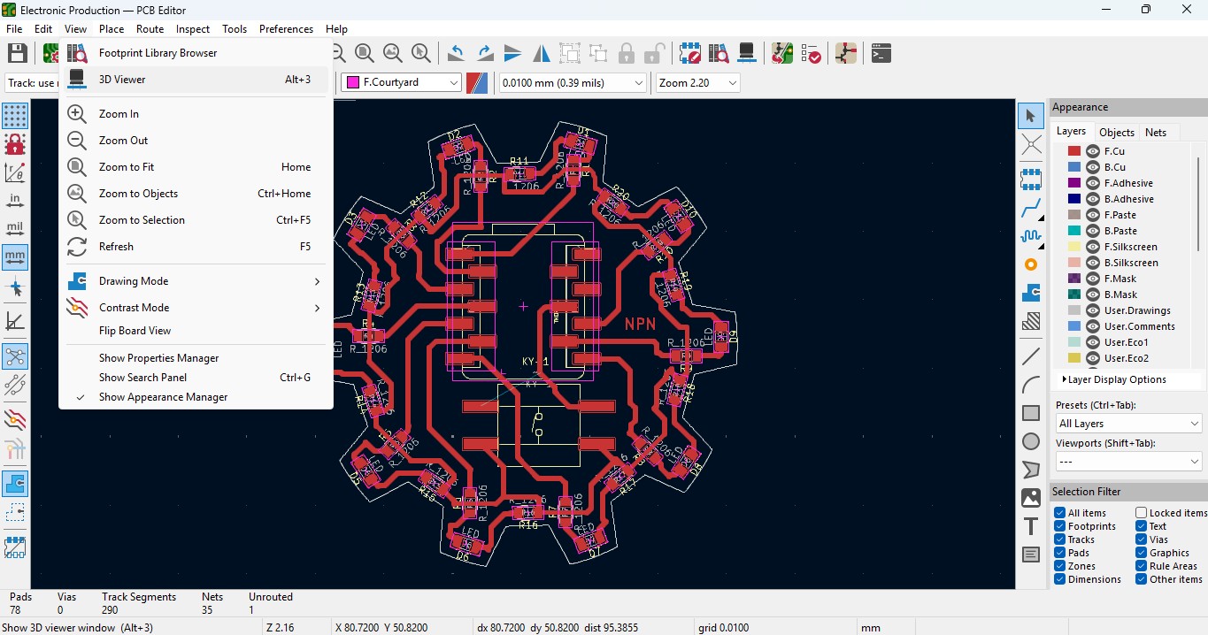
18. Place all the components in it and the design may look like this (This is my first time i made a peculiar design like this rather than greometric design)
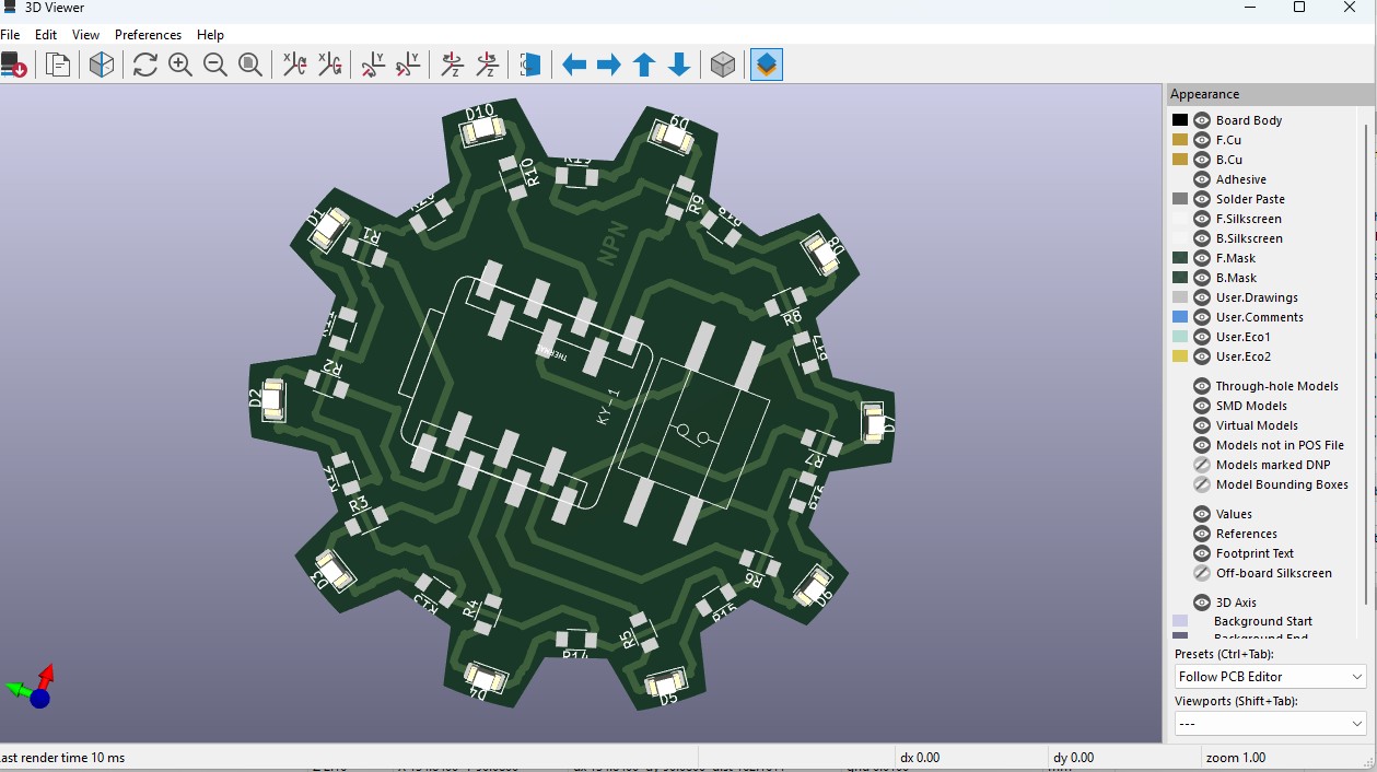
19. Go to view -> 3D Viewer adn click it.
20. you may view the 3D design of the model we made it in PCB design.
21. Now go back and go to File -> plot and click on it.
22. click on the layers that you may need in my case i need F.cu and edge cuts layers on it and click on teh output directory and change the directory on it.
23. click on the "Plot" button and the file has been generated.
Programming
// Define LED pins
const int ledPins[10] = {0, 1, 2, 3, 4, 5, 6, 7, 8, 9};
const int buttonPin = 10;

// Button and pattern control
int currentPattern = 0;
bool lastButtonState = HIGH;
bool buttonState = HIGH;
unsigned long lastDebounceTime = 0;
const unsigned long debounceDelay = 50;

void setup() {
  for (int i = 0; i < 10; i++) {
    pinMode(ledPins[i], OUTPUT);
    digitalWrite(ledPins[i], LOW); // Turn off all LEDs initially
  }
  pinMode(buttonPin, INPUT_PULLUP);

  Serial.begin(9600); // Optional: Enable serial debug
}

void loop() {
  // ---- Button debounce logic ----
  bool reading = digitalRead(buttonPin);

  if (reading != lastButtonState) {
    lastDebounceTime = millis(); // reset debounce timer
  }

  if ((millis() - lastDebounceTime) > debounceDelay) {
    if (reading != buttonState) {
      buttonState = reading;
      if (buttonState == LOW) {
        currentPattern = (currentPattern + 1) % 10; // Cycle through patterns
        Serial.print("Switched to pattern: ");
        Serial.println(currentPattern);
      }
    }
  }

  lastButtonState = reading;

  // ---- Run current pattern ----
  runPattern(currentPattern);
}

// --------------------- Pattern Selection ---------------------
void runPattern(int pattern) {
  switch (pattern) {
    case 0: patternChase(); break;
    case 1: patternBounce(); break;
    case 2: patternAllOn(); break;
    case 3: patternEvenOdd(); break;
    case 4: patternAlternateBlink(); break;
    case 5: patternFill(); break;
    case 6: patternFlashNonBlocking(); break; // <-- non-blocking version
    case 7: patternReverseChase(); break;
    case 8: patternMiddleOut(); break;
    case 9: patternWave(); break;
  }
}

// --------------------- Utility ---------------------
void clearLEDs() {
  for (int i = 0; i < 10; i++) {
    digitalWrite(ledPins[i], LOW);
  }
}

// --------------------- Pattern Functions ---------------------

void patternChase() {
  for (int i = 0; i < 10; i++) {
    clearLEDs();
    digitalWrite(ledPins[i], HIGH);
    delay(100);
  }
}

void patternBounce() {
  for (int i = 0; i < 10; i++) {
    clearLEDs();
    digitalWrite(ledPins[i], HIGH);
    delay(80);
  }
  for (int i = 8; i >= 1; i--) {
    clearLEDs();
    digitalWrite(ledPins[i], HIGH);
    delay(80);
  }
}

void patternAllOn() {
  for (int i = 0; i < 10; i++) {
    digitalWrite(ledPins[i], HIGH);
  }
  delay(500);
  clearLEDs();
  delay(500);
}

void patternEvenOdd() {
  clearLEDs();
  for (int i = 0; i < 10; i += 2) digitalWrite(ledPins[i], HIGH);
  delay(300);
  clearLEDs();
  for (int i = 1; i < 10; i += 2) digitalWrite(ledPins[i], HIGH);
  delay(300);
}

void patternAlternateBlink() {
  for (int j = 0; j < 2; j++) {
    for (int i = 0; i < 10; i++) digitalWrite(ledPins[i], (j % 2 == 0) ? HIGH : LOW);
    delay(300);
  }
  clearLEDs();
}

void patternFill() {
  for (int i = 0; i < 10; i++) {
    digitalWrite(ledPins[i], HIGH);
    delay(100);
  }
  delay(300);
  clearLEDs();
}

// ✅ Non-blocking version of flash pattern
void patternFlashNonBlocking() {
  static unsigned long lastUpdate = 0;
  static bool state = false;

  if (millis() - lastUpdate >= 200) {
    lastUpdate = millis();
    state = !state;
    for (int i = 0; i < 10; i++) {
      digitalWrite(ledPins[i], state ? HIGH : LOW);
    }
  }
}

void patternReverseChase() {
  for (int i = 9; i >= 0; i--) {
    clearLEDs();
    digitalWrite(ledPins[i], HIGH);
    delay(100);
  }
}

void patternMiddleOut() {
  int mid = 5;
  for (int offset = 0; offset < 5; offset++) {
    clearLEDs();
    digitalWrite(ledPins[mid - offset], HIGH);
    digitalWrite(ledPins[mid + offset], HIGH);
    delay(150);
  }
}

void patternWave() {
  for (int i = 0; i < 10; i++) {
    digitalWrite(ledPins[i], HIGH);
    delay(60);
    digitalWrite(ledPins[i], LOW);
  }
}
Download Files
Here, you can download the files that i made over this assignment
Laser Cutter Machine
1. Gerber files
2. FlatCAM File
2. G-Code File
4. click on the "Plot" button and the file has been generated.
Introduction to FlatCAM
FlatCAM is an open-source software tool used primarily for preparing PCB (Printed Circuit Board) designs for CNC milling. It takes Gerber files (generated by PCB design tools like KiCAD, Eagle, or Altium) and converts them into G-code, which can be used by a CNC machine to mill the PCB..
Installation of FlatCAM
1. Go to Google to Search "FlatCAM" to get the FlatCAM official website (www.flatcam.org) , Click on it .
2. in that Flatcam website -> sa you may see over there you may click download.
3. if you click over there and there will be lot of os version to download in there click it on Windows(as i having windows to use it).
4. in that you may see many version and in that download latest one in it.
Here is the link button below:
to download the FlatCAM version
Or you can download manually:
Click here to download KiCAD
Opening the software
After Opening the FlatCAM, a Window will pop up that is Main Windowand you are gonna work on it.
Converting Gerber files to G-CODE
1. This is the main window. you should use that in well about it.
2. click -> open -> open Gerber.
3. Click all the contents and "open" it.
4. as you seen over here, the contents will be displayed in it.
5. move all the file to the origin axis in it.
6. right click the file and -> move then move it.
7. Move all the contents in the Origin.
8. Click the F-CU copper gerber file and double click it.
9. In that There are many option to do in that We ahve to Click "Isolation Routing" that is this will isolate the route taht we need to do and it should be done for tracks in PCB. click on it.
10. In that there will be tools table in which we have to do is give bit diameter in it. after giving diameter in it just need to give the passes (how many layers of cut you may required) for mine i gave around 4and click "Generate Geometry"
11. After that you can clearly see that in which the diagram or your design is changed and having many layers.
12. In that change the V-tip size that is on 30 degree and overly mentioned that and spindle speed is should be around 10000 and click on "Generate CNCJob object".
13. as you have seen over there, everything has been done and you just need to save the g-code that has been generated that is by clicking "Save CNC code"
14. A small wiondow will pop up navigate where you wanna save, then click "save" to save it..
15. after completion for F-Cu file that is track file . let's do it for the outline file aslo in there by Double-clicking on it.
16. A window will pop up same as for track routing instead of selecting Isolation routing click "Cutout tool" in it to outer-cut the File.
17. another window will come that will be different from previous windows in that you have to generate the geomentry by giving tool diameter - that is 2.0 (its in our lab file) and give cut z to -1.8 and click "Generate Geometry" into it.
18. if you go to main window you may visit a new geometry in it. double click It .
19. it may look like similar window click on it and customize the value as you needed as in spindle speed that is 10000 and click "Generate CNCJob Object" that will create a structure..
20. you can clearly see and there will be a option to save by clicking "Save CNC Code" to save it.
21. A small window will pop up and navigate the path and there will be to save the file and click it.
22. As you have seen over here there are two files that is the G-code been generated.
PCB Milling Machine
PCB milling involves mechanically removing material from a copper-clad board to create electrical isolation and form circuit patterns. Unlike traditional etching methods, which use chemical solutions to dissolve unwanted copper, milling uses precision-controlled milling bits to physically carve out the desired traces. The process is typically carried out using a Computer Numerical Control (CNC) milling machine, which is programmed to follow a specific design layout to guarantee accuracy and repeatability.
1. Open the Kicad and main Window will pop up and go to File -> New Project
2. Browse the location and name the Project in my case i have added "electronic Production"
3. you may see the there are two files that is
- Schematic File (.sch)
- PCB Layout File (.kicad_pcb)
Idea generation of making Design
1. I though to make a design that is different from somethinga dn i need to be in circular so i searched for the many this i got an awesome idea to make a design that is CogWheel in it.
2. download a image and im gonna use Inkscape software to edit the design simailar to make it on.
3. and this is what i made from it and downloaded as a SVG file so that i can move it as a outline on my board
Making Schematic for your circuit
1. Open the Kicad and main Window will pop up abd click on the Schematic Editor
2. A new Window is pop up that is Schematic editor weher you make schematic diagrams for your circuit
3. By clicking "A" or click on the 3 option on the right panel that is "add components" to add new components. a new window will pop up
4. search of the components that you may required in it so in this assignment i wnat these components in it
Components required
- Seeed studio Xiao ESP32C3 module X 1
- SMD LED (1206) X 10
- SMD resistor 100 ohms (1206) X 10
- SMD resistor 0 ohms (1206) X 10
- KY - 004 Tactile switch X 1
So im searching the component LED in it.
5. place the components in it
6. Duplicate the contents as per your needs.
7. As you have seen that i have places all the components in it with its quantities
8. Arrange all the components as per the you convienent and i made it look like this in it
9. Give the Circuit Connection as per your need that is by clicking "w" or click on the 5 option on the right panel that is "wire" to give connections in it
10. After all the connections are given, the remaining not connected pins are needed to connect this pins that is "no connection flags" that is avaialbe on 8th block which is in on right panel.
11. after connection all that flags you may see like this connection .
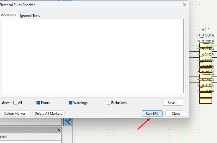
12. After all connection, go to Inspect -> Electrical Rules Checker. Click on it
13. A new window will pop up and it is mainly used to check if there is any issue or not . so do that click on "Run ERC"
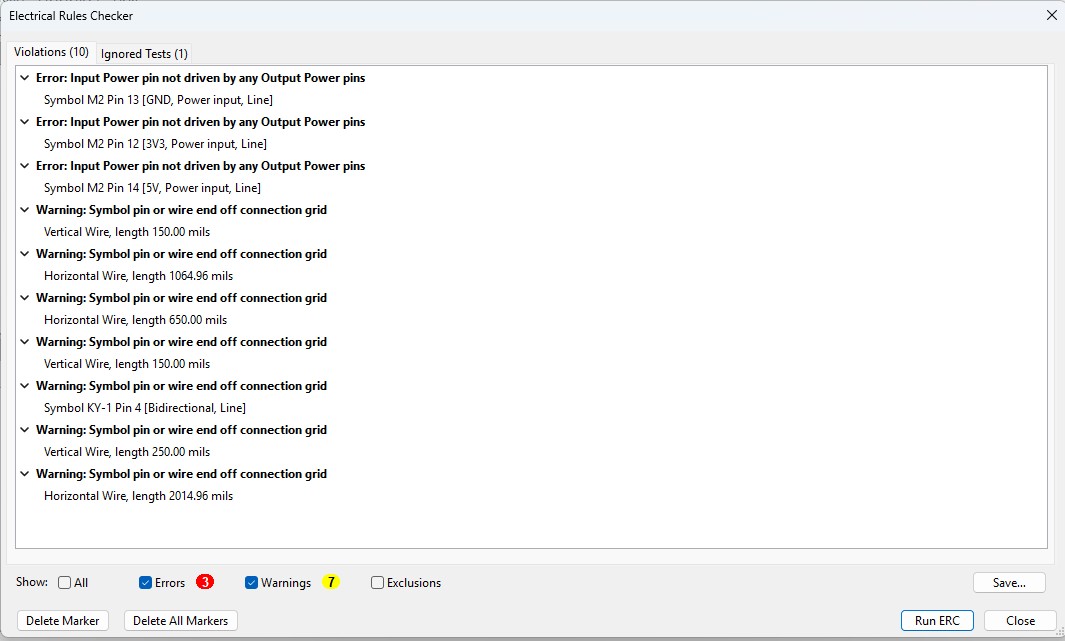
14. It may start to run checker and finds all the issue and error or warnings that are available in your circuit. so find all are correct are not.
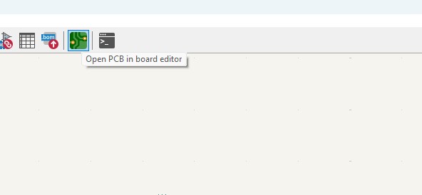
15. After doing all the things, click on the "Open PCB in board editor" to import the design from schematic design to pcb design.
Making PCB design from the Schematic Diagram
1. Open the Kicad and main Window will pop up abd click on the PCB Editor
2. This Windows is used for the PCB design that you make in schematic design.
3. Over top, you make see the symbol like that, that is used to update the PCB with changes taht made in schematic. so click that.
4. A new window will appear over that click on "Update PCB " button and all the components may list out over here click on it.
5. all the components are updated in the PCB editor and as you been seen over here.
6. Click File -> Import -> Graphics and click it to import Outline of the board.
7. A New Window will pop up and over there will be a changable dropdown go o there and click that to "Edge.Cuts" and click on the folder button change the directory.
8. A new window will come over there navigate the directory to the file where the SVG file is located and clicked on it.
9. The Edge cut outline gets out over here (as i used Cog Wheel in it) place it on.
10. Click on the component and double click it and "Footprint Properties" window may appear on the orientation and change the degree to the convienent way so that adjust it on and place it.
11. Place all the Led components in the teeth of the outline as i did.
12. place all the resistor and do the same for it also as did for LED in it and rearrange it.
13. Over the right panel there are all things, click on the fourth block that is "Route Tracks" or click on "X" to start the routing.
14. Over the left upper panel and click on the "Track: use netclass width" and change that to "edit pre-defined sizes" and click it.
15. A new window will pop up and click on (+)icon on the Track Column "width" and click on it.
16. Change that to the your wish track size so for me i gave it to 0.8mm track width size. and click it
17. Now click on th esame track width in there you may see track 0.800mm width size in it. click it.
18. Place all the components in it and the design may look like this (This is my first time i made a peculiar design like this rather than greometric design)
19. Go to view -> 3D Viewer adn click it.
20. you may view the 3D design of the model we made it in PCB design.
21. Now go back and go to File -> plot and click on it.
22. click on the layers that you may need in my case i need F.cu and edge cuts layers on it and click on teh output directory and change the directory on it.
23. click on the "Plot" button and the file has been generated.
Programming
// Define LED pins
const int ledPins[10] = {0, 1, 2, 3, 4, 5, 6, 7, 8, 9};
const int buttonPin = 10;
// Button and pattern control
int currentPattern = 0;
bool lastButtonState = HIGH;
bool buttonState = HIGH;
unsigned long lastDebounceTime = 0;
const unsigned long debounceDelay = 50;
void setup() {
for (int i = 0; i < 10; i++) {
pinMode(ledPins[i], OUTPUT);
digitalWrite(ledPins[i], LOW); // Turn off all LEDs initially
}
pinMode(buttonPin, INPUT_PULLUP);
Serial.begin(9600); // Optional: Enable serial debug
}
void loop() {
// ---- Button debounce logic ----
bool reading = digitalRead(buttonPin);
if (reading != lastButtonState) {
lastDebounceTime = millis(); // reset debounce timer
}
if ((millis() - lastDebounceTime) > debounceDelay) {
if (reading != buttonState) {
buttonState = reading;
if (buttonState == LOW) {
currentPattern = (currentPattern + 1) % 10; // Cycle through patterns
Serial.print("Switched to pattern: ");
Serial.println(currentPattern);
}
}
}
lastButtonState = reading;
// ---- Run current pattern ----
runPattern(currentPattern);
}
// --------------------- Pattern Selection ---------------------
void runPattern(int pattern) {
switch (pattern) {
case 0: patternChase(); break;
case 1: patternBounce(); break;
case 2: patternAllOn(); break;
case 3: patternEvenOdd(); break;
case 4: patternAlternateBlink(); break;
case 5: patternFill(); break;
case 6: patternFlashNonBlocking(); break; // <-- non-blocking version
case 7: patternReverseChase(); break;
case 8: patternMiddleOut(); break;
case 9: patternWave(); break;
}
}
// --------------------- Utility ---------------------
void clearLEDs() {
for (int i = 0; i < 10; i++) {
digitalWrite(ledPins[i], LOW);
}
}
// --------------------- Pattern Functions ---------------------
void patternChase() {
for (int i = 0; i < 10; i++) {
clearLEDs();
digitalWrite(ledPins[i], HIGH);
delay(100);
}
}
void patternBounce() {
for (int i = 0; i < 10; i++) {
clearLEDs();
digitalWrite(ledPins[i], HIGH);
delay(80);
}
for (int i = 8; i >= 1; i--) {
clearLEDs();
digitalWrite(ledPins[i], HIGH);
delay(80);
}
}
void patternAllOn() {
for (int i = 0; i < 10; i++) {
digitalWrite(ledPins[i], HIGH);
}
delay(500);
clearLEDs();
delay(500);
}
void patternEvenOdd() {
clearLEDs();
for (int i = 0; i < 10; i += 2) digitalWrite(ledPins[i], HIGH);
delay(300);
clearLEDs();
for (int i = 1; i < 10; i += 2) digitalWrite(ledPins[i], HIGH);
delay(300);
}
void patternAlternateBlink() {
for (int j = 0; j < 2; j++) {
for (int i = 0; i < 10; i++) digitalWrite(ledPins[i], (j % 2 == 0) ? HIGH : LOW);
delay(300);
}
clearLEDs();
}
void patternFill() {
for (int i = 0; i < 10; i++) {
digitalWrite(ledPins[i], HIGH);
delay(100);
}
delay(300);
clearLEDs();
}
// ✅ Non-blocking version of flash pattern
void patternFlashNonBlocking() {
static unsigned long lastUpdate = 0;
static bool state = false;
if (millis() - lastUpdate >= 200) {
lastUpdate = millis();
state = !state;
for (int i = 0; i < 10; i++) {
digitalWrite(ledPins[i], state ? HIGH : LOW);
}
}
}
void patternReverseChase() {
for (int i = 9; i >= 0; i--) {
clearLEDs();
digitalWrite(ledPins[i], HIGH);
delay(100);
}
}
void patternMiddleOut() {
int mid = 5;
for (int offset = 0; offset < 5; offset++) {
clearLEDs();
digitalWrite(ledPins[mid - offset], HIGH);
digitalWrite(ledPins[mid + offset], HIGH);
delay(150);
}
}
void patternWave() {
for (int i = 0; i < 10; i++) {
digitalWrite(ledPins[i], HIGH);
delay(60);
digitalWrite(ledPins[i], LOW);
}
}
Download Files
Here, you can download the files that i made over this assignment
Laser Cutter Machine
1. Gerber files
2. FlatCAM File
2. G-Code File
Click here to download KiCAD
8. Click the F-CU copper gerber file and double click it.
9. In that There are many option to do in that We ahve to Click "Isolation Routing" that is this will isolate the route taht we need to do and it should be done for tracks in PCB. click on it.
10. In that there will be tools table in which we have to do is give bit diameter in it. after giving diameter in it just need to give the passes (how many layers of cut you may required) for mine i gave around 4and click "Generate Geometry"
11. After that you can clearly see that in which the diagram or your design is changed and having many layers.
12. In that change the V-tip size that is on 30 degree and overly mentioned that and spindle speed is should be around 10000 and click on "Generate CNCJob object".
13. as you have seen over there, everything has been done and you just need to save the g-code that has been generated that is by clicking "Save CNC code"
14. A small wiondow will pop up navigate where you wanna save, then click "save" to save it..
15. after completion for F-Cu file that is track file . let's do it for the outline file aslo in there by Double-clicking on it.
16. A window will pop up same as for track routing instead of selecting Isolation routing click "Cutout tool" in it to outer-cut the File.
17. another window will come that will be different from previous windows in that you have to generate the geomentry by giving tool diameter - that is 2.0 (its in our lab file) and give cut z to -1.8 and click "Generate Geometry" into it.
18. if you go to main window you may visit a new geometry in it. double click It .
19. it may look like similar window click on it and customize the value as you needed as in spindle speed that is 10000 and click "Generate CNCJob Object" that will create a structure..
20. you can clearly see and there will be a option to save by clicking "Save CNC Code" to save it.
21. A small window will pop up and navigate the path and there will be to save the file and click it.
22. As you have seen over here there are two files that is the G-code been generated.
PCB Milling Machine
PCB milling involves mechanically removing material from a copper-clad board to create electrical isolation and form circuit patterns. Unlike traditional etching methods, which use chemical solutions to dissolve unwanted copper, milling uses precision-controlled milling bits to physically carve out the desired traces. The process is typically carried out using a Computer Numerical Control (CNC) milling machine, which is programmed to follow a specific design layout to guarantee accuracy and repeatability.
1. Open the Kicad and main Window will pop up and go to File -> New Project
2. Browse the location and name the Project in my case i have added "electronic Production"
3. you may see the there are two files that is
- Schematic File (.sch)
- PCB Layout File (.kicad_pcb)
Idea generation of making Design
1. I though to make a design that is different from somethinga dn i need to be in circular so i searched for the many this i got an awesome idea to make a design that is CogWheel in it.
2. download a image and im gonna use Inkscape software to edit the design simailar to make it on.
3. and this is what i made from it and downloaded as a SVG file so that i can move it as a outline on my board
Making Schematic for your circuit
1. Open the Kicad and main Window will pop up abd click on the Schematic Editor
2. A new Window is pop up that is Schematic editor weher you make schematic diagrams for your circuit
3. By clicking "A" or click on the 3 option on the right panel that is "add components" to add new components. a new window will pop up
4. search of the components that you may required in it so in this assignment i wnat these components in it
Components required
- Seeed studio Xiao ESP32C3 module X 1
- SMD LED (1206) X 10
- SMD resistor 100 ohms (1206) X 10
- SMD resistor 0 ohms (1206) X 10
- KY - 004 Tactile switch X 1
So im searching the component LED in it.
5. place the components in it
6. Duplicate the contents as per your needs.
7. As you have seen that i have places all the components in it with its quantities
8. Arrange all the components as per the you convienent and i made it look like this in it
9. Give the Circuit Connection as per your need that is by clicking "w" or click on the 5 option on the right panel that is "wire" to give connections in it
10. After all the connections are given, the remaining not connected pins are needed to connect this pins that is "no connection flags" that is avaialbe on 8th block which is in on right panel.
11. after connection all that flags you may see like this connection .
12. After all connection, go to Inspect -> Electrical Rules Checker. Click on it
13. A new window will pop up and it is mainly used to check if there is any issue or not . so do that click on "Run ERC"
14. It may start to run checker and finds all the issue and error or warnings that are available in your circuit. so find all are correct are not.
15. After doing all the things, click on the "Open PCB in board editor" to import the design from schematic design to pcb design.
Making PCB design from the Schematic Diagram
1. Open the Kicad and main Window will pop up abd click on the PCB Editor
2. This Windows is used for the PCB design that you make in schematic design.
3. Over top, you make see the symbol like that, that is used to update the PCB with changes taht made in schematic. so click that.
4. A new window will appear over that click on "Update PCB " button and all the components may list out over here click on it.
5. all the components are updated in the PCB editor and as you been seen over here.
6. Click File -> Import -> Graphics and click it to import Outline of the board.
7. A New Window will pop up and over there will be a changable dropdown go o there and click that to "Edge.Cuts" and click on the folder button change the directory.
8. A new window will come over there navigate the directory to the file where the SVG file is located and clicked on it.
9. The Edge cut outline gets out over here (as i used Cog Wheel in it) place it on.
10. Click on the component and double click it and "Footprint Properties" window may appear on the orientation and change the degree to the convienent way so that adjust it on and place it.
11. Place all the Led components in the teeth of the outline as i did.
12. place all the resistor and do the same for it also as did for LED in it and rearrange it.
13. Over the right panel there are all things, click on the fourth block that is "Route Tracks" or click on "X" to start the routing.
14. Over the left upper panel and click on the "Track: use netclass width" and change that to "edit pre-defined sizes" and click it.
15. A new window will pop up and click on (+)icon on the Track Column "width" and click on it.
16. Change that to the your wish track size so for me i gave it to 0.8mm track width size. and click it
17. Now click on th esame track width in there you may see track 0.800mm width size in it. click it.
18. Place all the components in it and the design may look like this (This is my first time i made a peculiar design like this rather than greometric design)
19. Go to view -> 3D Viewer adn click it.
20. you may view the 3D design of the model we made it in PCB design.
21. Now go back and go to File -> plot and click on it.
22. click on the layers that you may need in my case i need F.cu and edge cuts layers on it and click on teh output directory and change the directory on it.
23. click on the "Plot" button and the file has been generated.
Programming
// Define LED pins
const int ledPins[10] = {0, 1, 2, 3, 4, 5, 6, 7, 8, 9};
const int buttonPin = 10;
// Button and pattern control
int currentPattern = 0;
bool lastButtonState = HIGH;
bool buttonState = HIGH;
unsigned long lastDebounceTime = 0;
const unsigned long debounceDelay = 50;
void setup() {
for (int i = 0; i < 10; i++) {
pinMode(ledPins[i], OUTPUT);
digitalWrite(ledPins[i], LOW); // Turn off all LEDs initially
}
pinMode(buttonPin, INPUT_PULLUP);
Serial.begin(9600); // Optional: Enable serial debug
}
void loop() {
// ---- Button debounce logic ----
bool reading = digitalRead(buttonPin);
if (reading != lastButtonState) {
lastDebounceTime = millis(); // reset debounce timer
}
if ((millis() - lastDebounceTime) > debounceDelay) {
if (reading != buttonState) {
buttonState = reading;
if (buttonState == LOW) {
currentPattern = (currentPattern + 1) % 10; // Cycle through patterns
Serial.print("Switched to pattern: ");
Serial.println(currentPattern);
}
}
}
lastButtonState = reading;
// ---- Run current pattern ----
runPattern(currentPattern);
}
// --------------------- Pattern Selection ---------------------
void runPattern(int pattern) {
switch (pattern) {
case 0: patternChase(); break;
case 1: patternBounce(); break;
case 2: patternAllOn(); break;
case 3: patternEvenOdd(); break;
case 4: patternAlternateBlink(); break;
case 5: patternFill(); break;
case 6: patternFlashNonBlocking(); break; // <-- non-blocking version
case 7: patternReverseChase(); break;
case 8: patternMiddleOut(); break;
case 9: patternWave(); break;
}
}
// --------------------- Utility ---------------------
void clearLEDs() {
for (int i = 0; i < 10; i++) {
digitalWrite(ledPins[i], LOW);
}
}
// --------------------- Pattern Functions ---------------------
void patternChase() {
for (int i = 0; i < 10; i++) {
clearLEDs();
digitalWrite(ledPins[i], HIGH);
delay(100);
}
}
void patternBounce() {
for (int i = 0; i < 10; i++) {
clearLEDs();
digitalWrite(ledPins[i], HIGH);
delay(80);
}
for (int i = 8; i >= 1; i--) {
clearLEDs();
digitalWrite(ledPins[i], HIGH);
delay(80);
}
}
void patternAllOn() {
for (int i = 0; i < 10; i++) {
digitalWrite(ledPins[i], HIGH);
}
delay(500);
clearLEDs();
delay(500);
}
void patternEvenOdd() {
clearLEDs();
for (int i = 0; i < 10; i += 2) digitalWrite(ledPins[i], HIGH);
delay(300);
clearLEDs();
for (int i = 1; i < 10; i += 2) digitalWrite(ledPins[i], HIGH);
delay(300);
}
void patternAlternateBlink() {
for (int j = 0; j < 2; j++) {
for (int i = 0; i < 10; i++) digitalWrite(ledPins[i], (j % 2 == 0) ? HIGH : LOW);
delay(300);
}
clearLEDs();
}
void patternFill() {
for (int i = 0; i < 10; i++) {
digitalWrite(ledPins[i], HIGH);
delay(100);
}
delay(300);
clearLEDs();
}
// ✅ Non-blocking version of flash pattern
void patternFlashNonBlocking() {
static unsigned long lastUpdate = 0;
static bool state = false;
if (millis() - lastUpdate >= 200) {
lastUpdate = millis();
state = !state;
for (int i = 0; i < 10; i++) {
digitalWrite(ledPins[i], state ? HIGH : LOW);
}
}
}
void patternReverseChase() {
for (int i = 9; i >= 0; i--) {
clearLEDs();
digitalWrite(ledPins[i], HIGH);
delay(100);
}
}
void patternMiddleOut() {
int mid = 5;
for (int offset = 0; offset < 5; offset++) {
clearLEDs();
digitalWrite(ledPins[mid - offset], HIGH);
digitalWrite(ledPins[mid + offset], HIGH);
delay(150);
}
}
void patternWave() {
for (int i = 0; i < 10; i++) {
digitalWrite(ledPins[i], HIGH);
delay(60);
digitalWrite(ledPins[i], LOW);
}
}
Download Files
Here, you can download the files that i made over this assignment
Laser Cutter Machine
1. Gerber files
2. FlatCAM File
2. G-Code File
// Define LED pins
const int ledPins[10] = {0, 1, 2, 3, 4, 5, 6, 7, 8, 9};
const int buttonPin = 10;
// Button and pattern control
int currentPattern = 0;
bool lastButtonState = HIGH;
bool buttonState = HIGH;
unsigned long lastDebounceTime = 0;
const unsigned long debounceDelay = 50;
void setup() {
for (int i = 0; i < 10; i++) {
pinMode(ledPins[i], OUTPUT);
digitalWrite(ledPins[i], LOW); // Turn off all LEDs initially
}
pinMode(buttonPin, INPUT_PULLUP);
Serial.begin(9600); // Optional: Enable serial debug
}
void loop() {
// ---- Button debounce logic ----
bool reading = digitalRead(buttonPin);
if (reading != lastButtonState) {
lastDebounceTime = millis(); // reset debounce timer
}
if ((millis() - lastDebounceTime) > debounceDelay) {
if (reading != buttonState) {
buttonState = reading;
if (buttonState == LOW) {
currentPattern = (currentPattern + 1) % 10; // Cycle through patterns
Serial.print("Switched to pattern: ");
Serial.println(currentPattern);
}
}
}
lastButtonState = reading;
// ---- Run current pattern ----
runPattern(currentPattern);
}
// --------------------- Pattern Selection ---------------------
void runPattern(int pattern) {
switch (pattern) {
case 0: patternChase(); break;
case 1: patternBounce(); break;
case 2: patternAllOn(); break;
case 3: patternEvenOdd(); break;
case 4: patternAlternateBlink(); break;
case 5: patternFill(); break;
case 6: patternFlashNonBlocking(); break; // <-- non-blocking version
case 7: patternReverseChase(); break;
case 8: patternMiddleOut(); break;
case 9: patternWave(); break;
}
}
// --------------------- Utility ---------------------
void clearLEDs() {
for (int i = 0; i < 10; i++) {
digitalWrite(ledPins[i], LOW);
}
}
// --------------------- Pattern Functions ---------------------
void patternChase() {
for (int i = 0; i < 10; i++) {
clearLEDs();
digitalWrite(ledPins[i], HIGH);
delay(100);
}
}
void patternBounce() {
for (int i = 0; i < 10; i++) {
clearLEDs();
digitalWrite(ledPins[i], HIGH);
delay(80);
}
for (int i = 8; i >= 1; i--) {
clearLEDs();
digitalWrite(ledPins[i], HIGH);
delay(80);
}
}
void patternAllOn() {
for (int i = 0; i < 10; i++) {
digitalWrite(ledPins[i], HIGH);
}
delay(500);
clearLEDs();
delay(500);
}
void patternEvenOdd() {
clearLEDs();
for (int i = 0; i < 10; i += 2) digitalWrite(ledPins[i], HIGH);
delay(300);
clearLEDs();
for (int i = 1; i < 10; i += 2) digitalWrite(ledPins[i], HIGH);
delay(300);
}
void patternAlternateBlink() {
for (int j = 0; j < 2; j++) {
for (int i = 0; i < 10; i++) digitalWrite(ledPins[i], (j % 2 == 0) ? HIGH : LOW);
delay(300);
}
clearLEDs();
}
void patternFill() {
for (int i = 0; i < 10; i++) {
digitalWrite(ledPins[i], HIGH);
delay(100);
}
delay(300);
clearLEDs();
}
// ✅ Non-blocking version of flash pattern
void patternFlashNonBlocking() {
static unsigned long lastUpdate = 0;
static bool state = false;
if (millis() - lastUpdate >= 200) {
lastUpdate = millis();
state = !state;
for (int i = 0; i < 10; i++) {
digitalWrite(ledPins[i], state ? HIGH : LOW);
}
}
}
void patternReverseChase() {
for (int i = 9; i >= 0; i--) {
clearLEDs();
digitalWrite(ledPins[i], HIGH);
delay(100);
}
}
void patternMiddleOut() {
int mid = 5;
for (int offset = 0; offset < 5; offset++) {
clearLEDs();
digitalWrite(ledPins[mid - offset], HIGH);
digitalWrite(ledPins[mid + offset], HIGH);
delay(150);
}
}
void patternWave() {
for (int i = 0; i < 10; i++) {
digitalWrite(ledPins[i], HIGH);
delay(60);
digitalWrite(ledPins[i], LOW);
}
}