Assignment
Group assignment:
- Compare as many tool options as possible.
- Document your work on the group page and reflect what you learned on your individual page.
Individual assignments:
- Write an application for the embedded board that you made. that interfaces a user with an input and/or output device(s).
Group Assigment
we compared many tools and learned many things on it.
Click on this button to get it to our Group Assignment Page
Individual Assignment
heroshot
This is my first time i made this type of Design and i love this one with all the design i made in it.
Introduction to KiCAD
KiCad is a free, open-source EDA tool used to design electronic circuits and PCBs. It offers features like schematic capture, PCB layout, 3D viewing, and Gerber file export, making it popular among engineers and hobbyists for turning ideas into working hardware.
Installation of KiCAD
1. Go to Google to Search "Kicad" to get the KiCad official website (www.kicad.org) , Click on it .

2. in that KiCad website -> click on Download Button.

3. you have to select the operation system in which you wanna install. i have windows operating system so select "Windows".

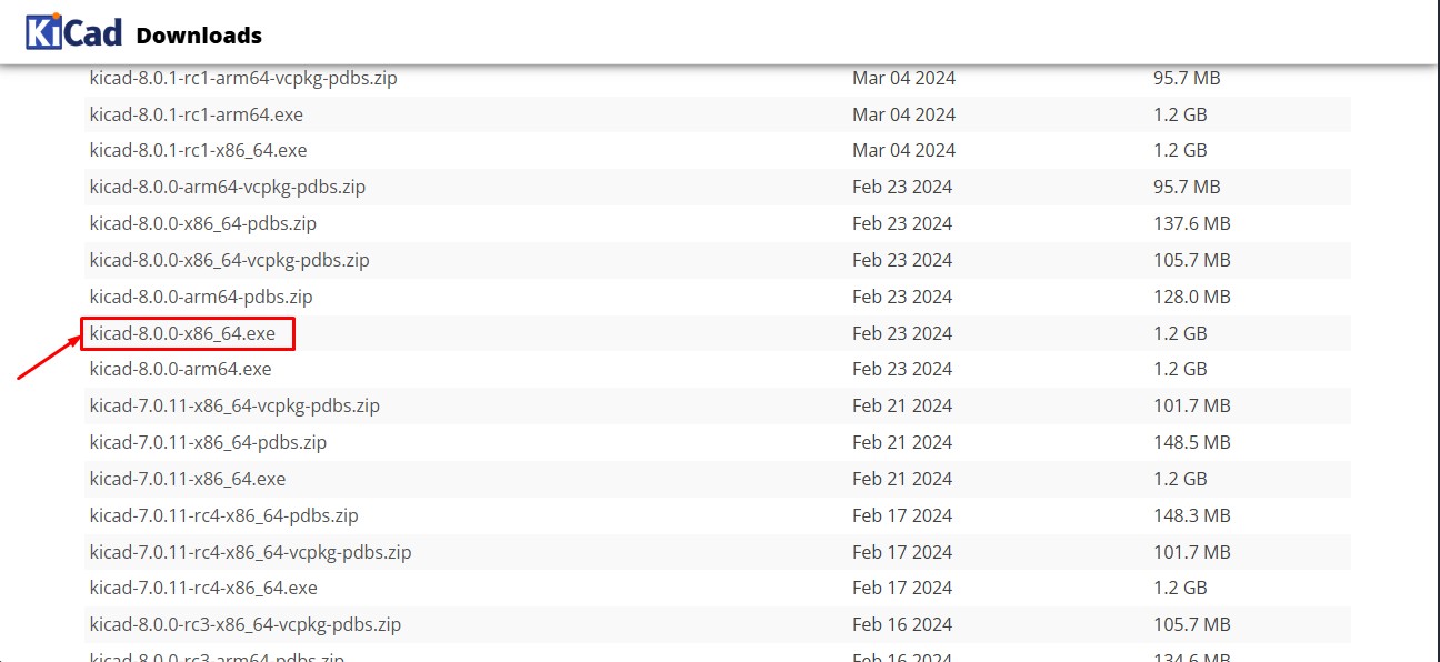
4. in that you can select the newest version to download but i want to install a specific old version of Kicad due to its feature that has been stopped after that versions. so that click on the "Previous Releases" link

5. in the all previous version click on "Kicad-8.0.0 x84x64.exe" as because that version and before has a feature that allows to download a pcb designs in SVG format. which is convenient to use that in online method that is called "modsproject" to milling the designs.
Here is the link button below:
to download the KiCAD 8.0 version
Or you can download manually:
Click here to download KiCAD
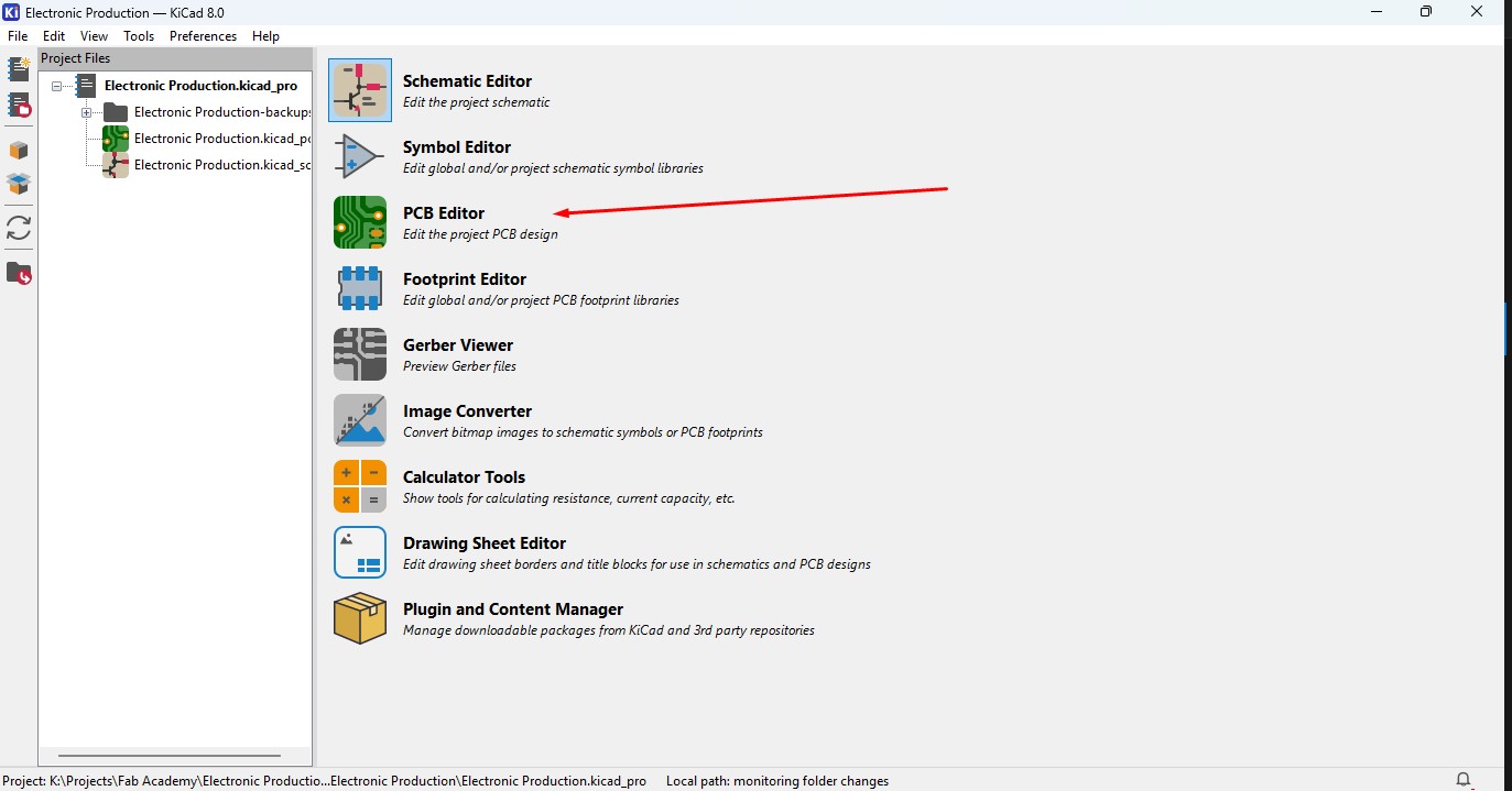
opening the software
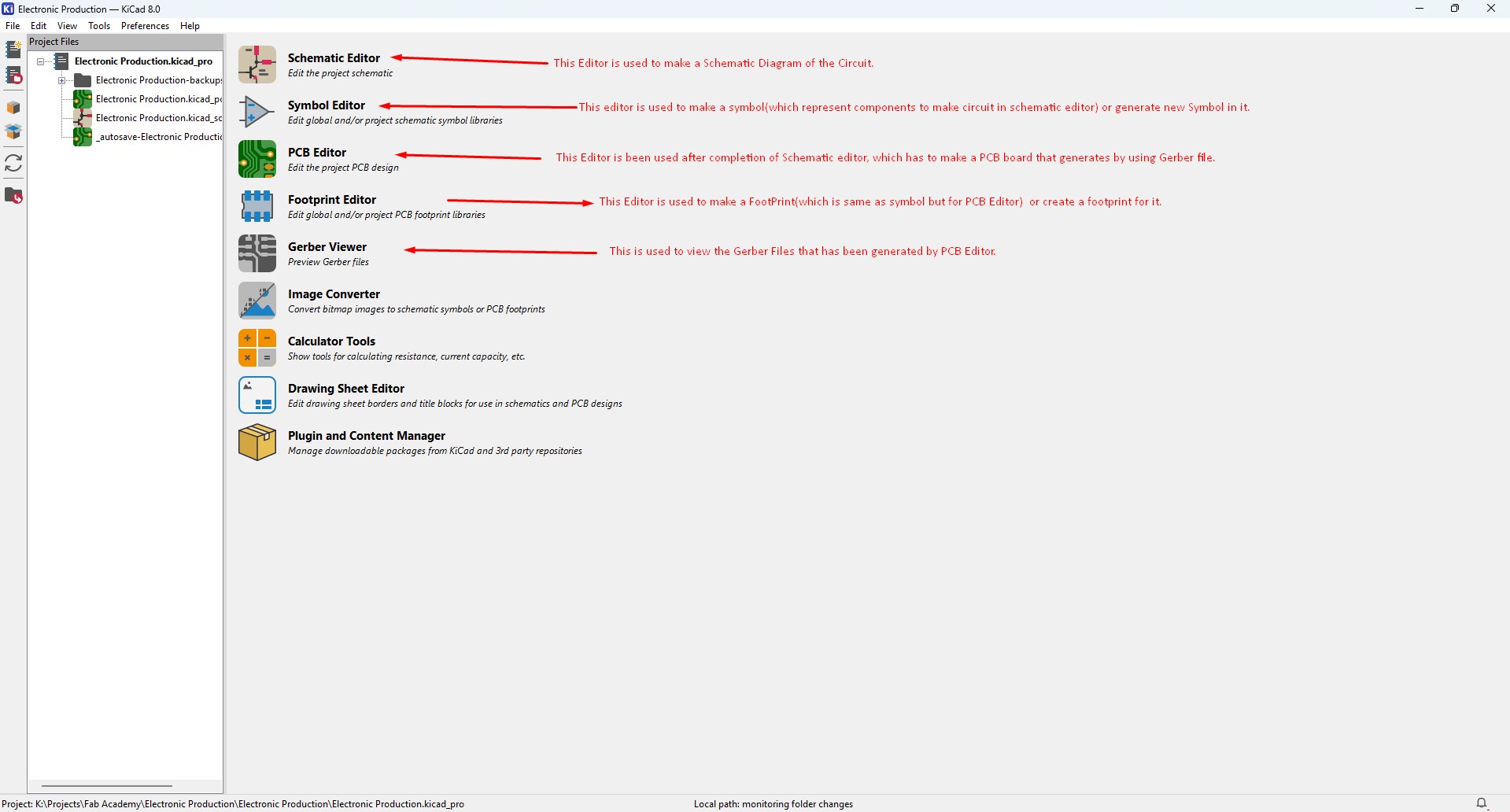
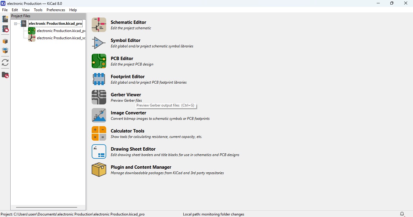
Opening the KiCad sofware will get a Main window that contains this contents that is Schematic Editor , Symbol Editor , PCB editor , Footprint editor , Gerber viewer
Downloading the Fab libraries
1. go to google and search fab kicad library, you may get a "fabcloud.org" link where you can download library. click on it

2. you may see like similar to gitlab as you see there from there you have to download all of these then. click on "CODE" button.
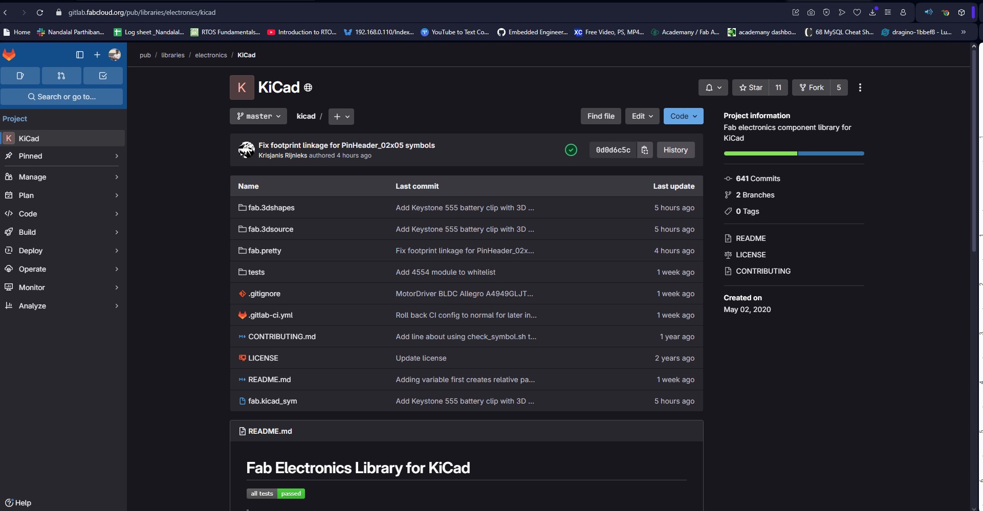
3. from there click ZIP to download zip file of the library
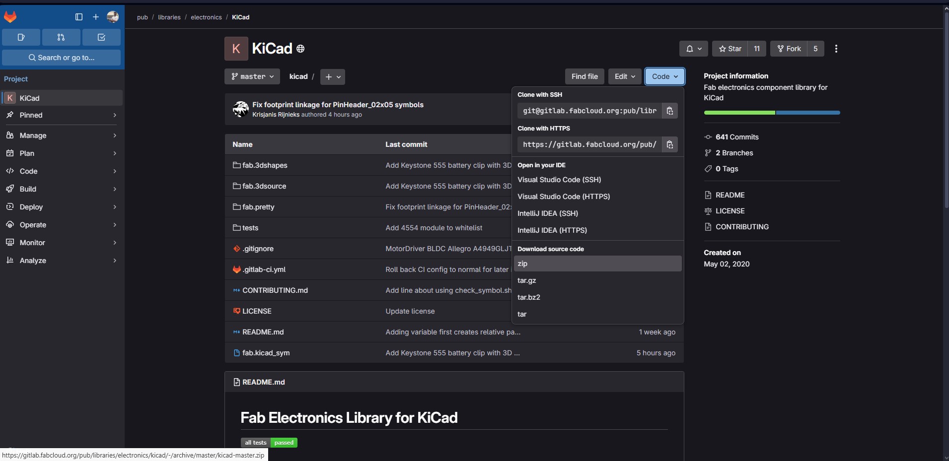
4. click on the file adn extract it on the file folder that you may remember.
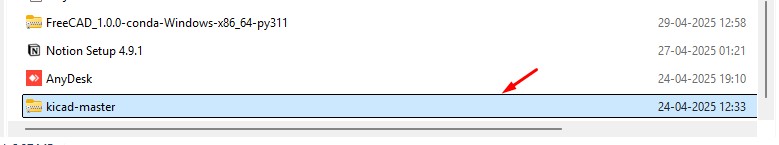
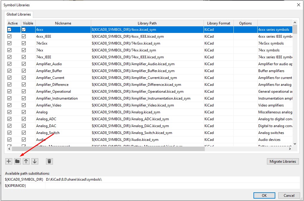
5. Go to KiCad Main window in that click Perference -> Manage Symbol Libraries and click on it.
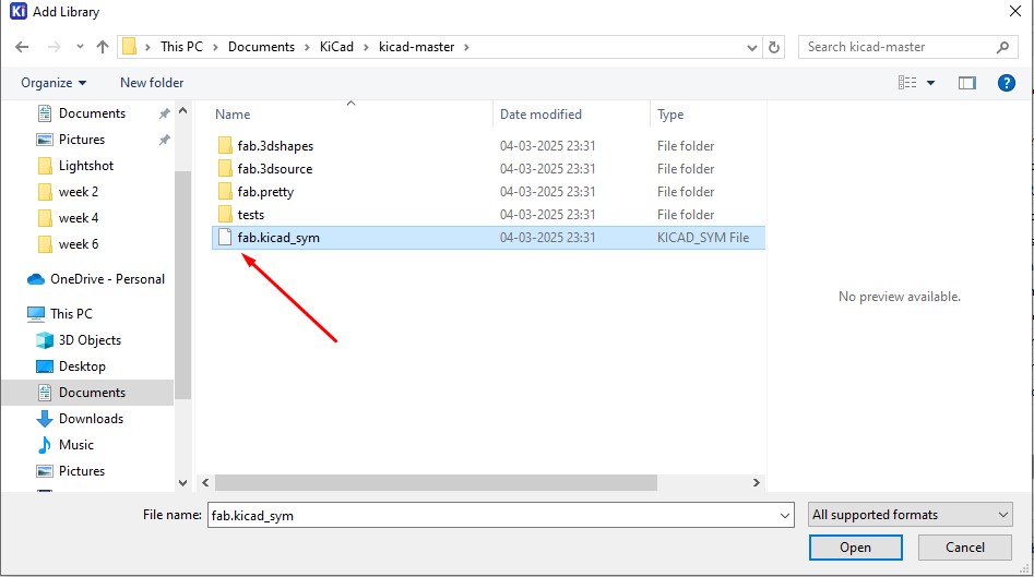
6. Click on the New Folder that will open up a new window.
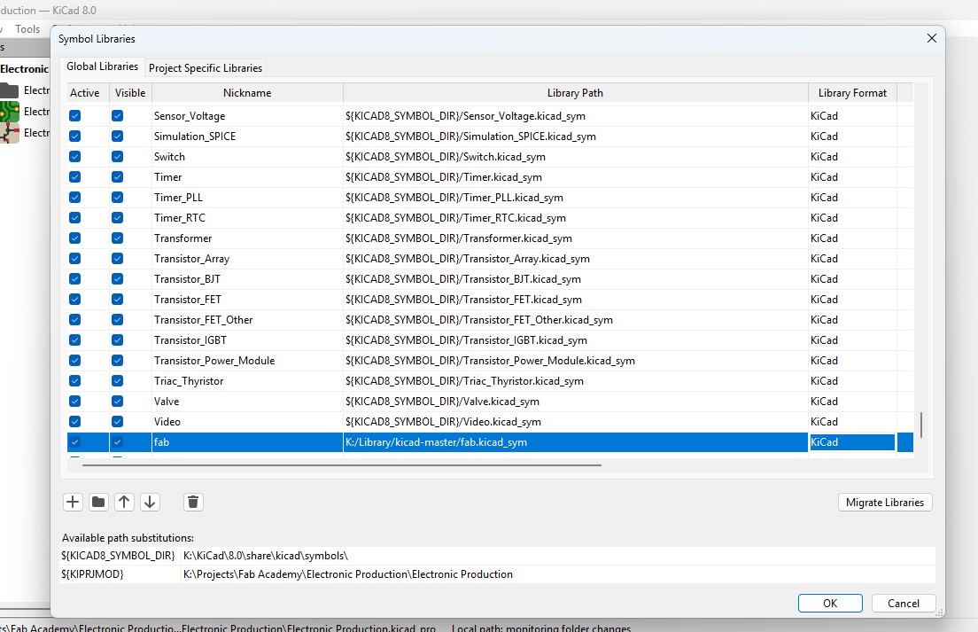
7. Navigate through and get the extracted "Kicad-master" folder and ensure that "fab.kicad_sym" has been clicked to upload that into the symbol editor
8. After the important that file you amy get to know that it has been uploaded and you visibly can see.
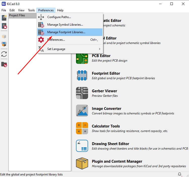
9. Now, come back to the same main window of the KiCad and go to Perferences-> Manage Footprint libraries.
10. there will be a window similar to symbol editor but in this we are gonna add footprint datas into it. go to Add (+) button and Click on it. write a Name that is Nickmake(which should be the same name that is already been allocated in symbol editor while add new symbol).
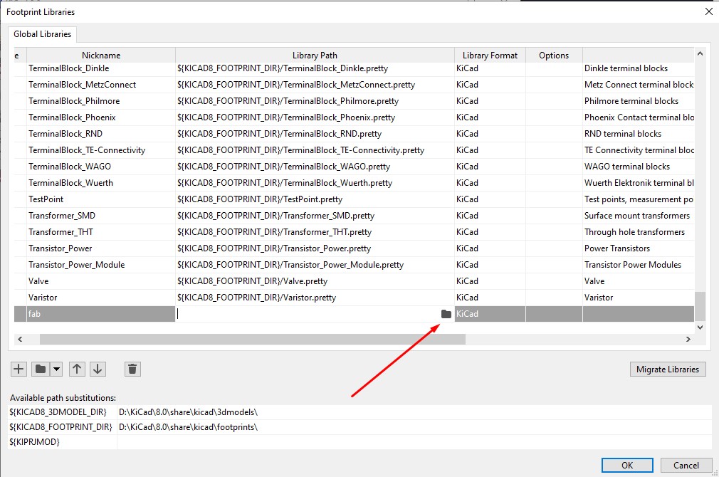
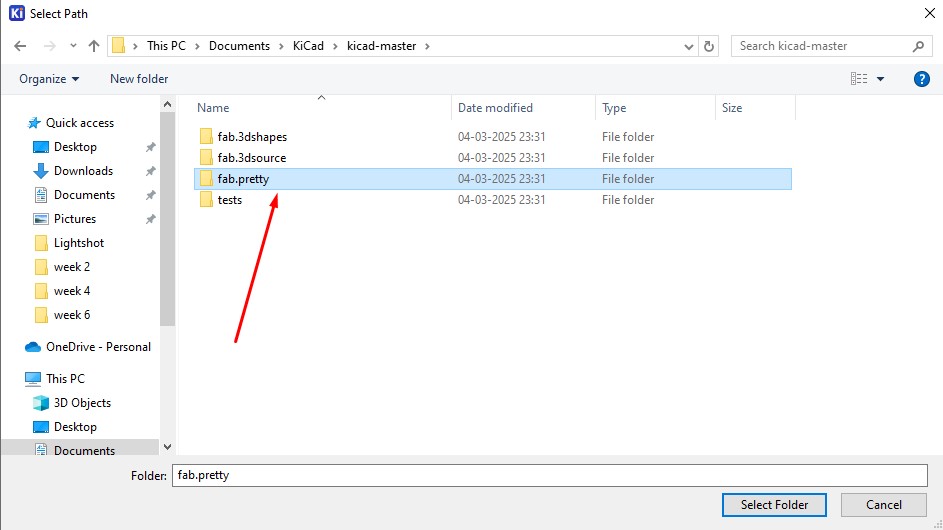
11. Navigate through and get the extracted "Kicad-master" folder and ensure that "fab.pretty"folder has been clicked to upload that into the footprint editor.
12. After the important that file you amy get to know that it has been uploaded and you visibly can see.

Here is the link button below:
Or you can download manually:
Click here to got to the Library link
Creating New Project
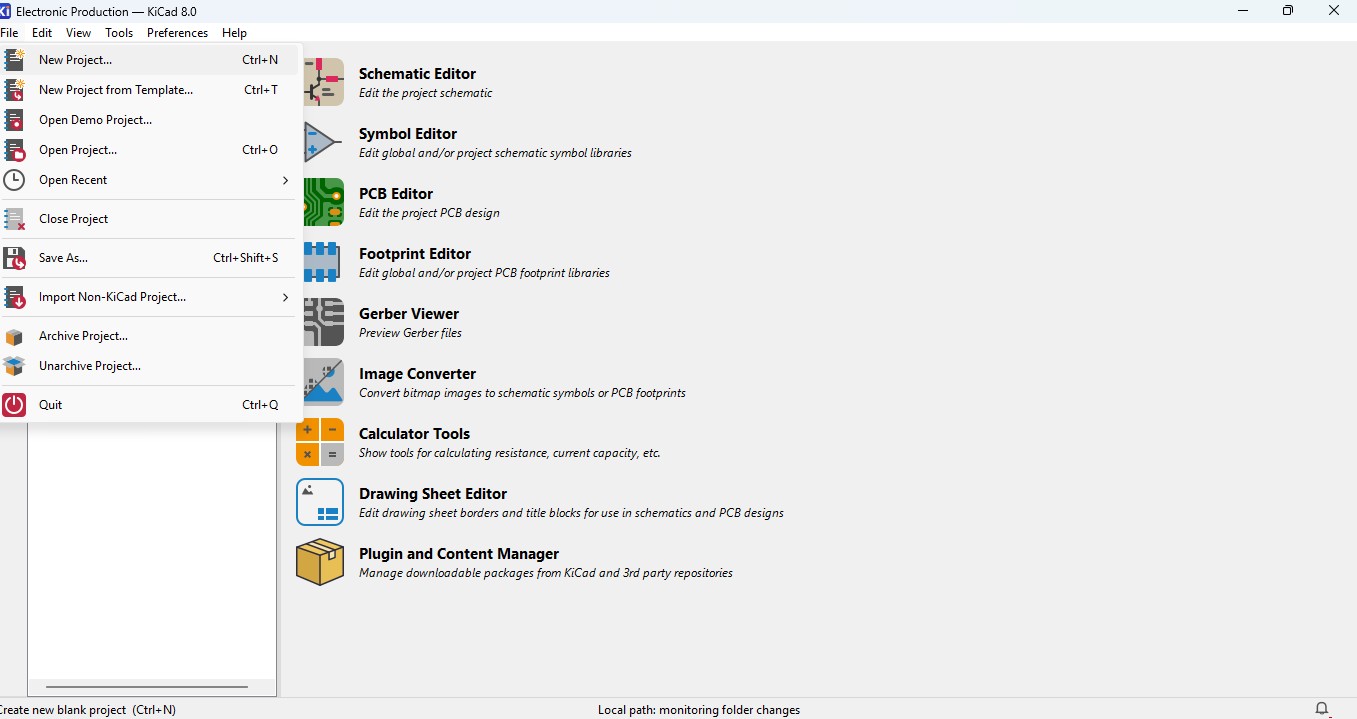
1. Open the Kicad and main Window will pop up and go to File -> New Project
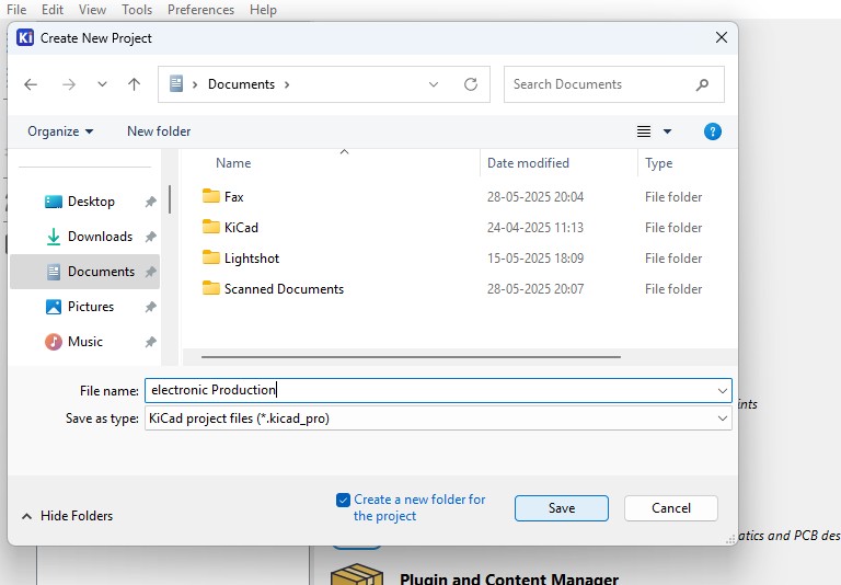
2. Browse the location and name the Project in my case i have added "electronic Production"
3. you may see the there are two files that is
- Schematic File (.sch)
- PCB Layout File (.kicad_pcb)
Idea generation of making Design
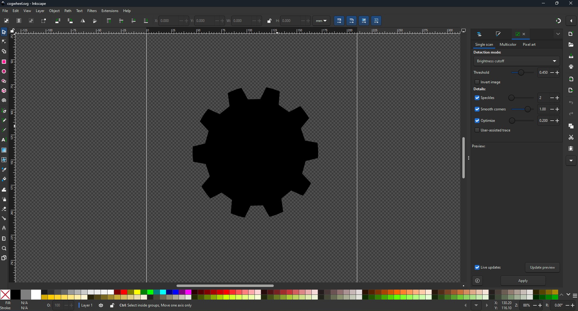
1. I though to make a design that is different from somethinga dn i need to be in circular so i searched for the many this i got an awesome idea to make a design that is CogWheel in it.

2. download a image and im gonna use Inkscape software to edit the design simailar to make it on.
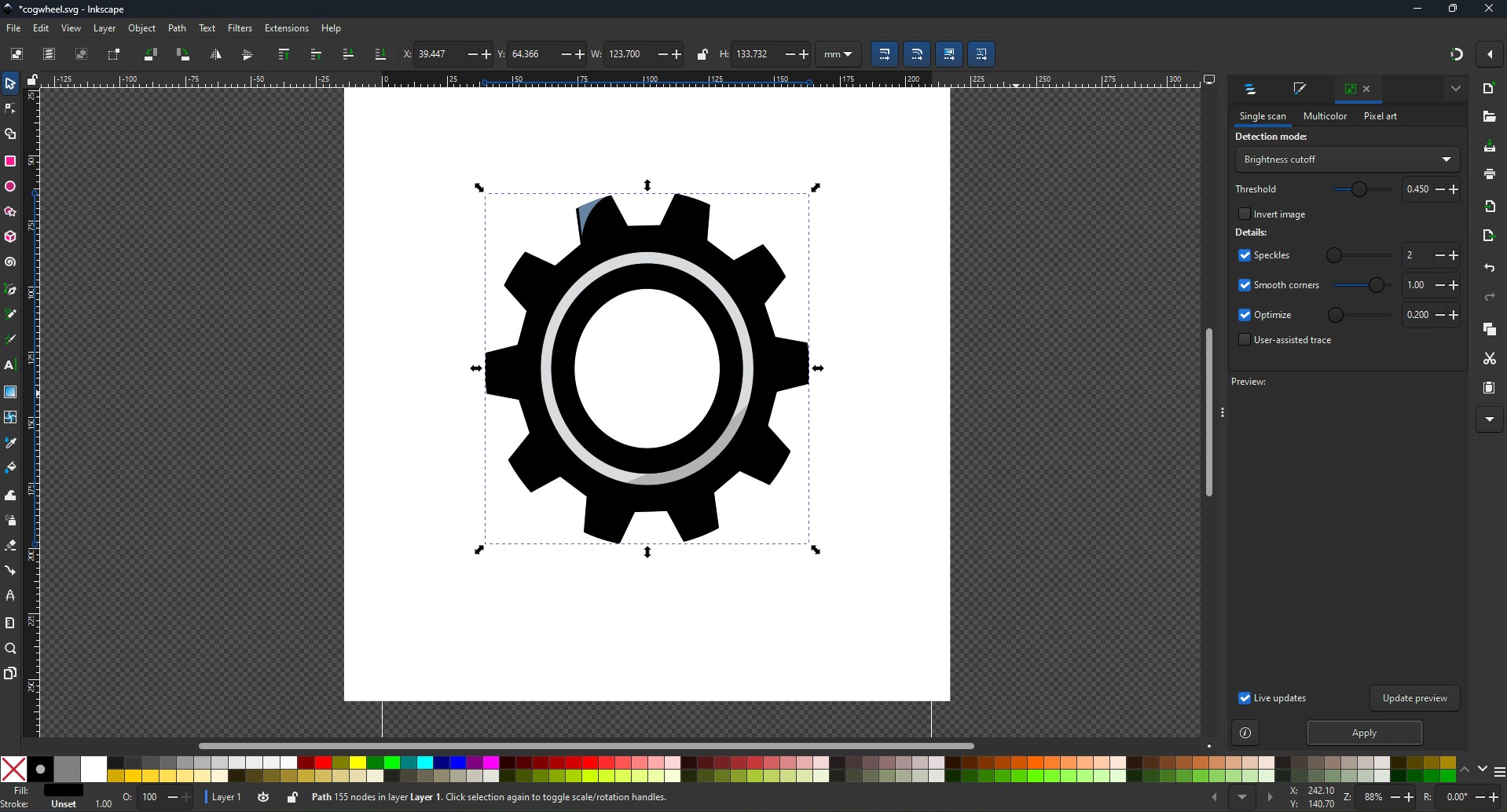
3. and this is what i made from it and downloaded as a SVG file so that i can move it as a outline on my board
Making Schematic for your circuit
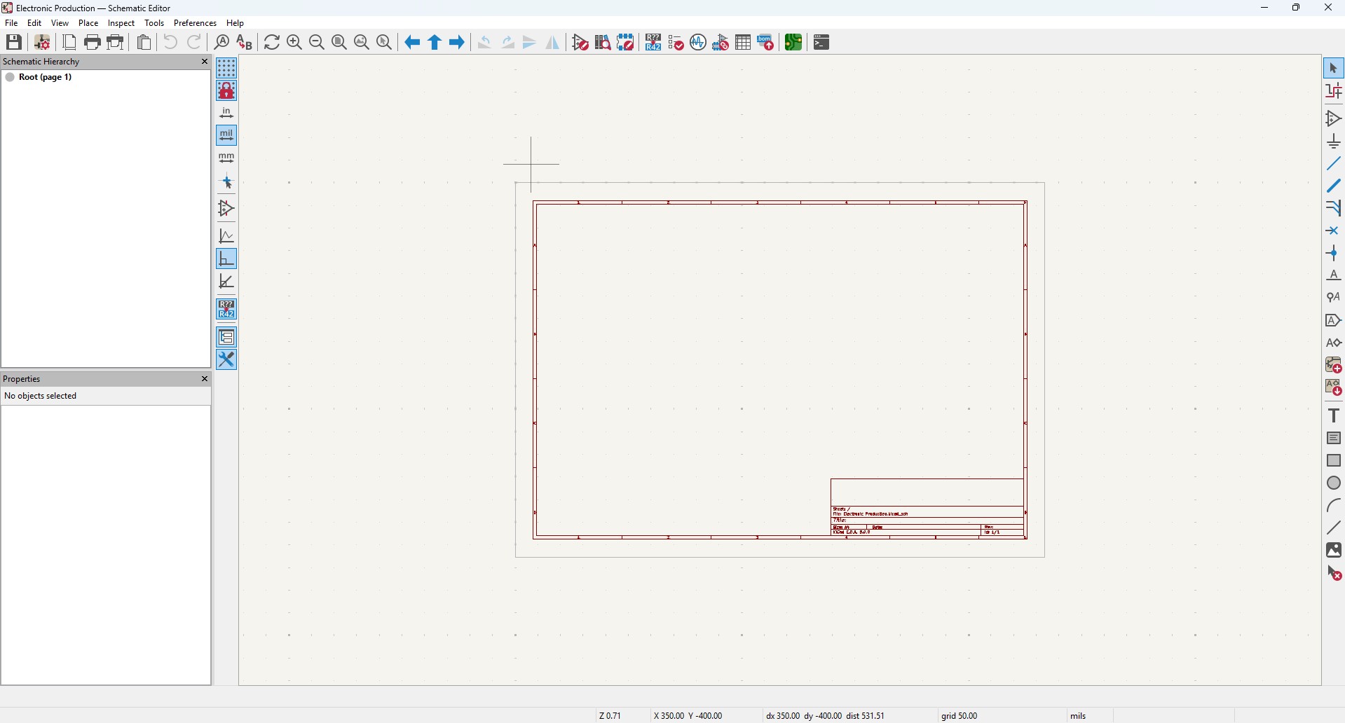
1. Open the Kicad and main Window will pop up abd click on the Schematic Editor
2. A new Window is pop up that is Schematic editor weher you make schematic diagrams for your circuit
3. By clicking "A" or click on the 3 option on the right panel that is "add components" to add new components. a new window will pop up
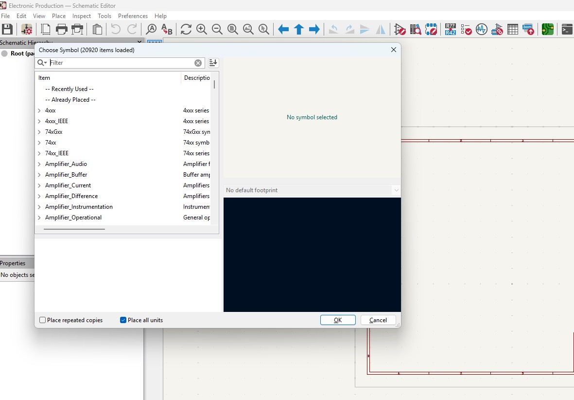
4. search of the components that you may required in it so in this assignment i wnat these components in it
Components required
- Seeed studio Xiao ESP32C3 module X 1
- SMD LED (1206) X 10
- SMD resistor 100 ohms (1206) X 10
- SMD resistor 0 ohms (1206) X 10
- KY - 004 Tactile switch X 1
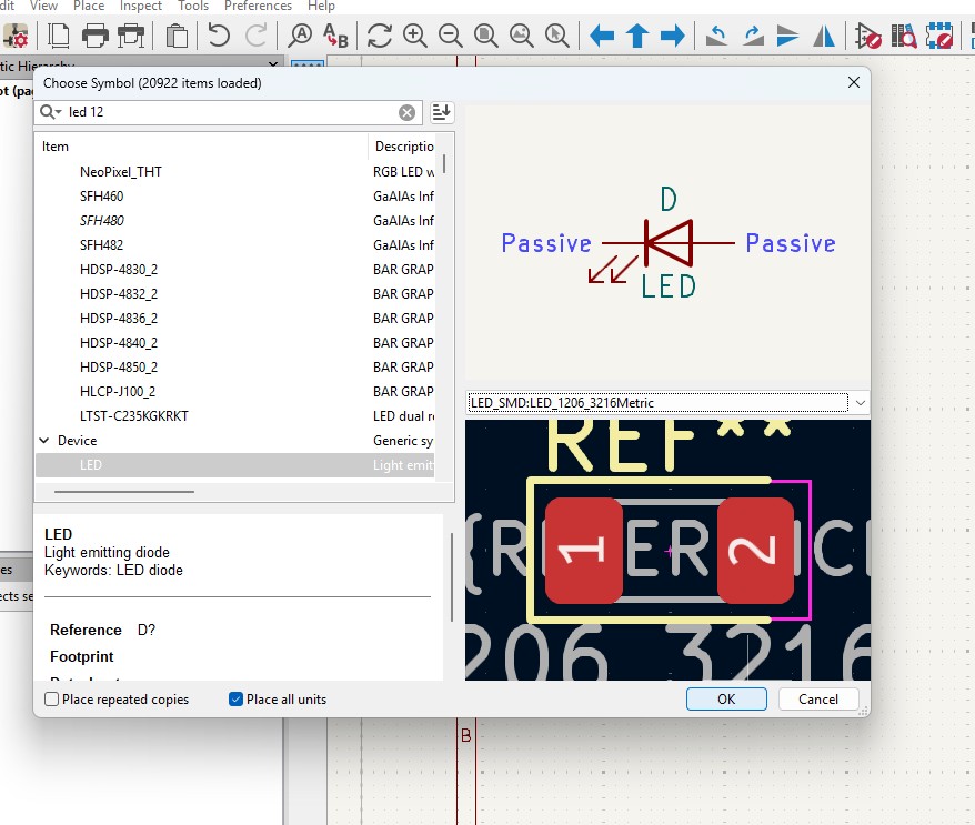
So im searching the component LED in it.
5. place the components in it
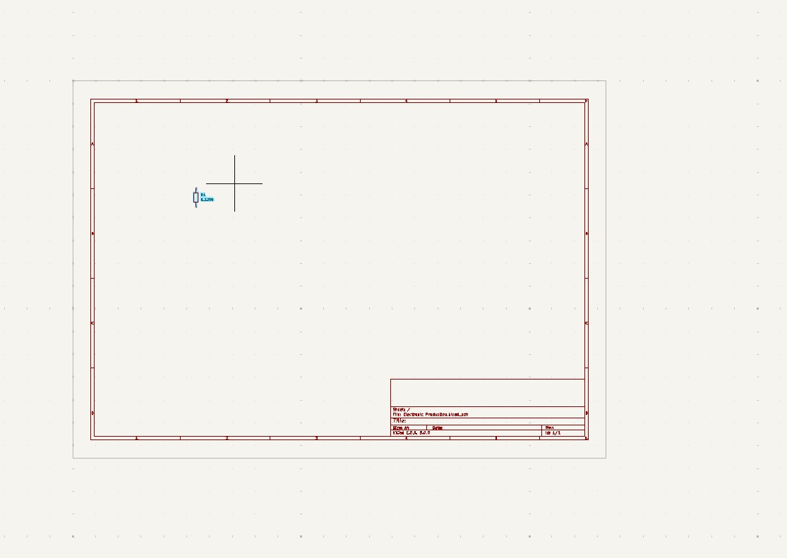
6. Duplicate the contents as per your needs.

7. As you have seen that i have places all the components in it with its quantities
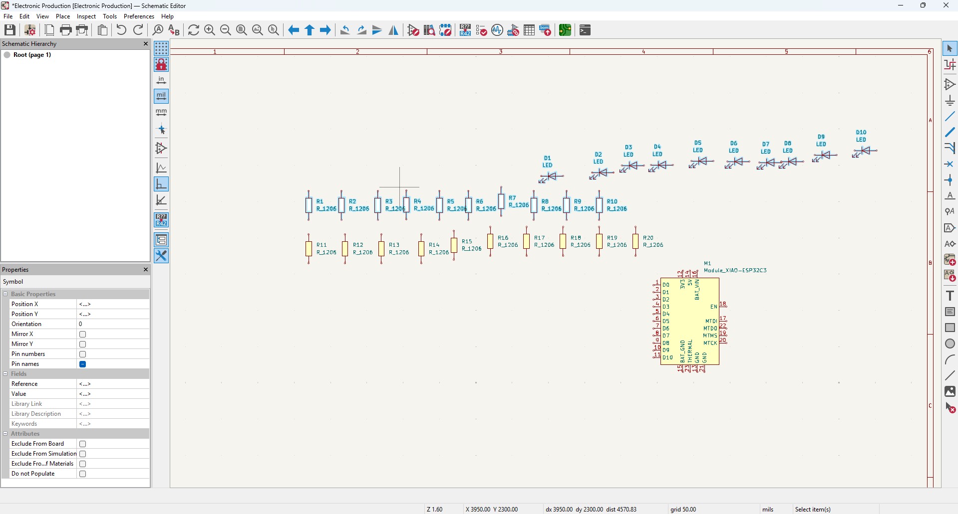
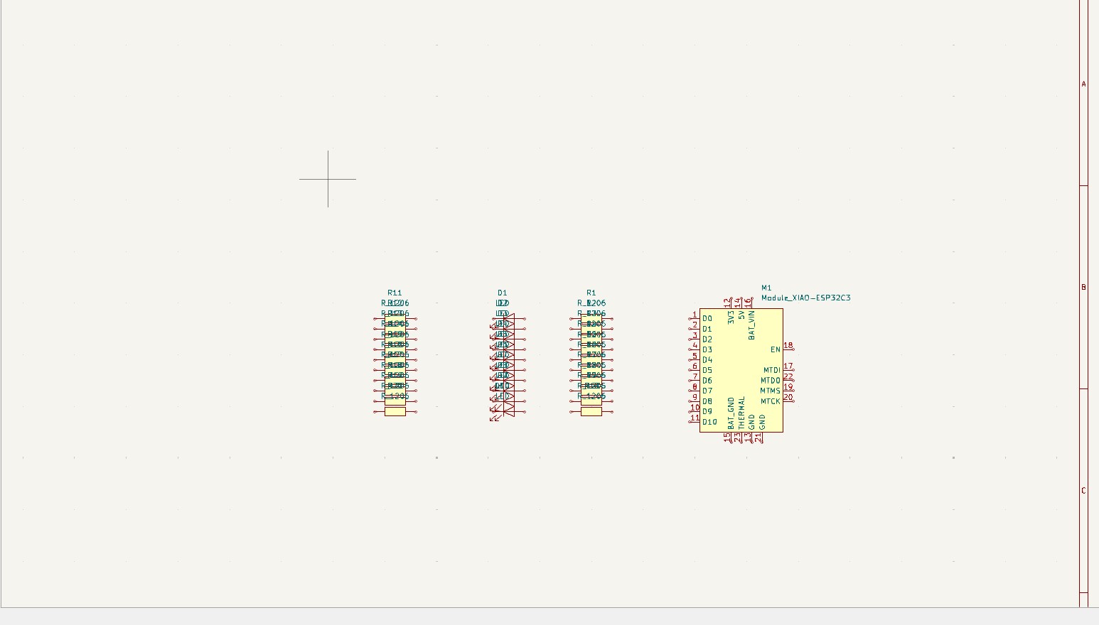
8. Arrange all the components as per the you convienent and i made it look like this in it
9. Give the Circuit Connection as per your need that is by clicking "w" or click on the 5 option on the right panel that is "wire" to give connections in it
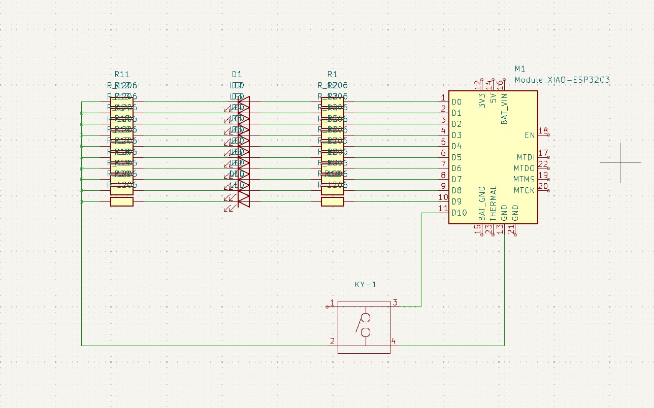
10. After all the connections are given, the remaining not connected pins are needed to connect this pins that is "no connection flags" that is avaialbe on 8th block which is in on right panel.
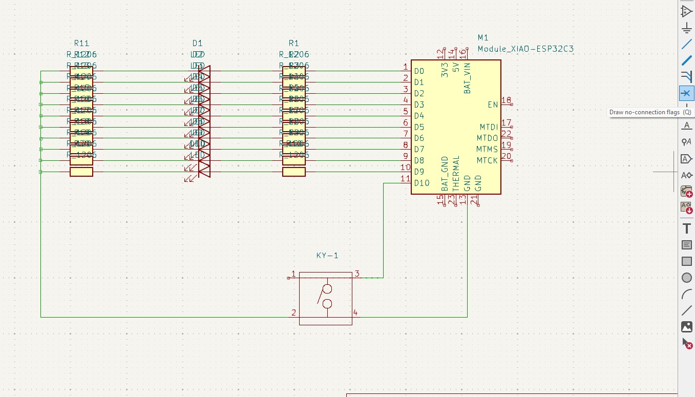
11. after connection all that flags you may see like this connection .
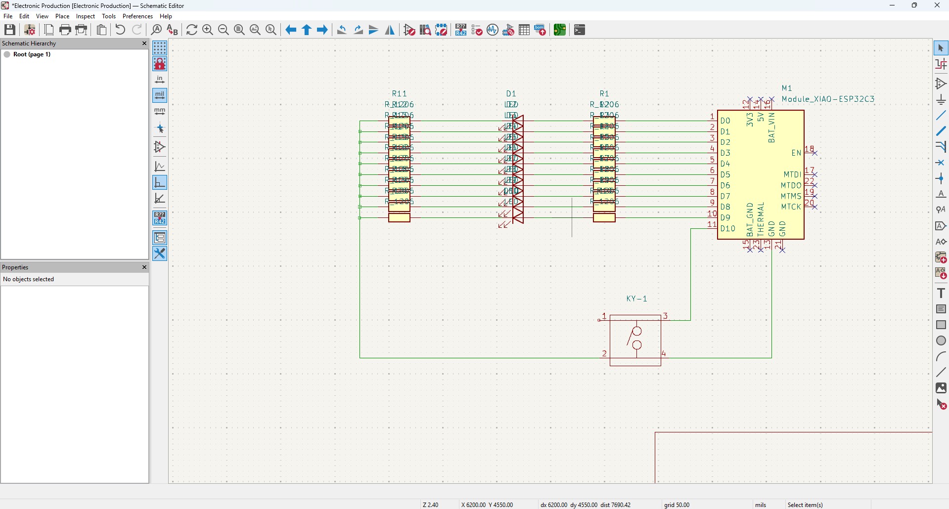
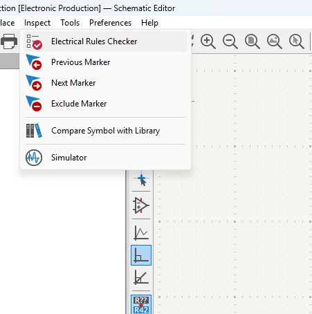
12. After all connection, go to Inspect -> Electrical Rules Checker. Click on it
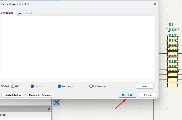
13. A new window will pop up and it is mainly used to check if there is any issue or not . so do that click on "Run ERC"
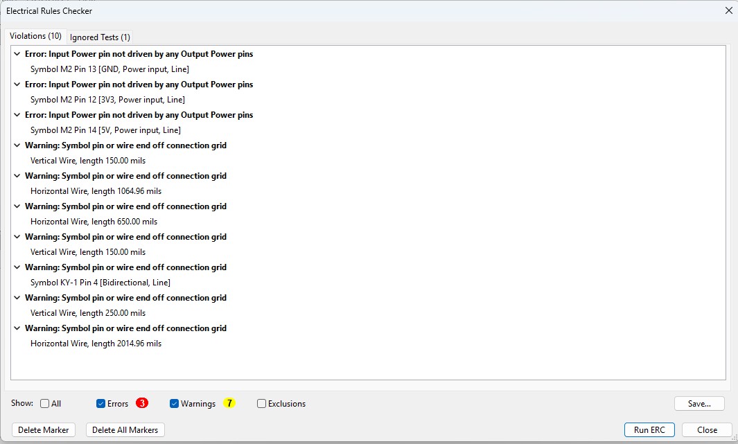
14. It may start to run checker and finds all the issue and error or warnings that are available in your circuit. so find all are correct are not.
15. After doing all the things, click on the "Open PCB in board editor" to import the design from schematic design to pcb design.
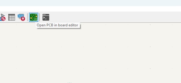
Making PCB design from the Schematic Diagram
1. Open the Kicad and main Window will pop up abd click on the PCB Editor
2. This Windows is used for the PCB design that you make in schematic design.

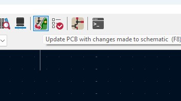
3. Over top, you make see the symbol like that, that is used to update the PCB with changes taht made in schematic. so click that.
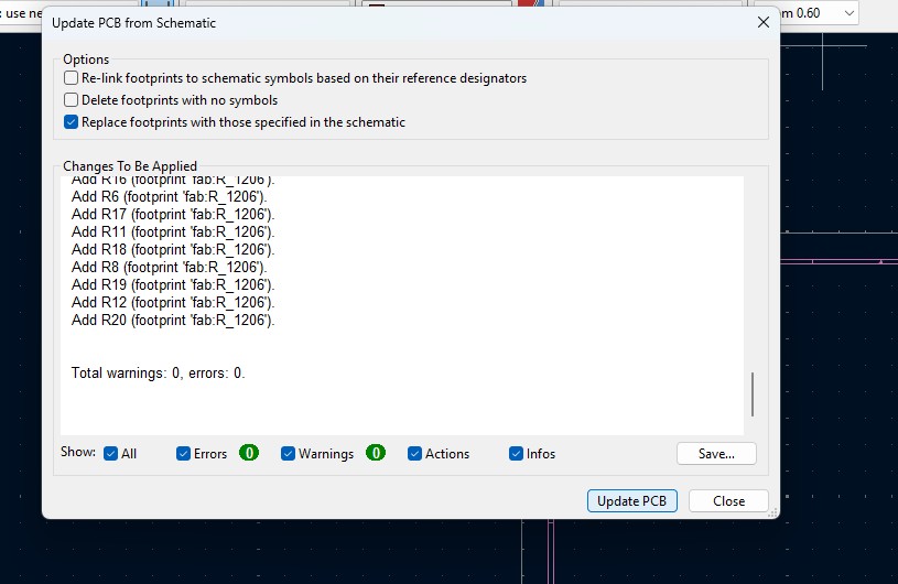
4. A new window will appear over that click on "Update PCB " button and all the components may list out over here click on it.
5. all the components are updated in the PCB editor and as you been seen over here.
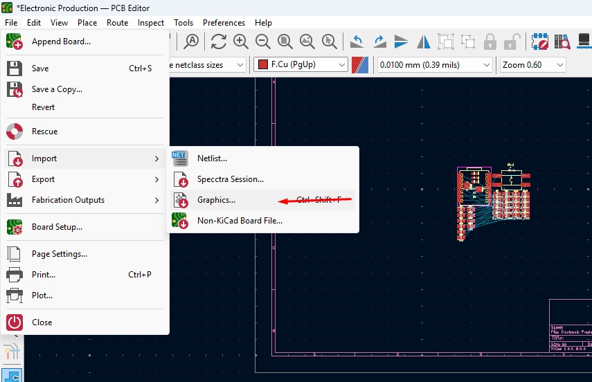
6. Click File -> Import -> Graphics and click it to import Outline of the board.
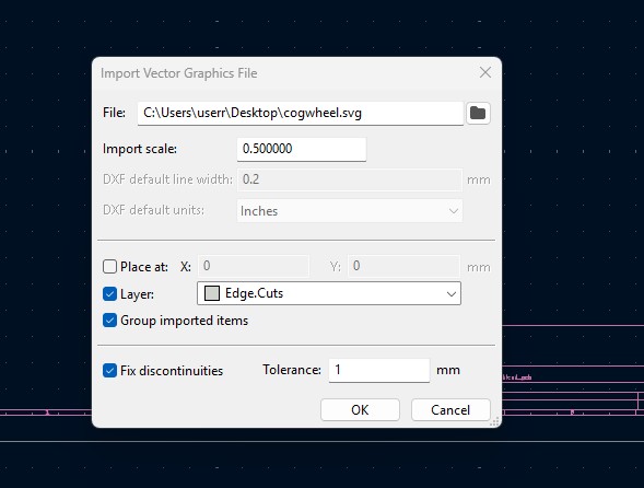
7. A New Window will pop up and over there will be a changable dropdown go o there and click that to "Edge.Cuts" and click on the folder button change the directory.
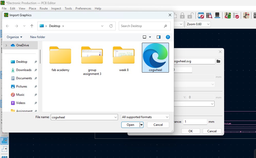
8. A new window will come over there navigate the directory to the file where the SVG file is located and clicked on it.
9. The Edge cut outline gets out over here (as i used Cog Wheel in it) place it on.
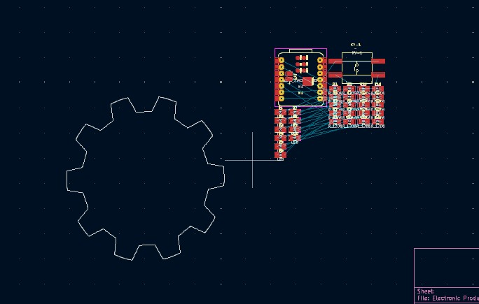
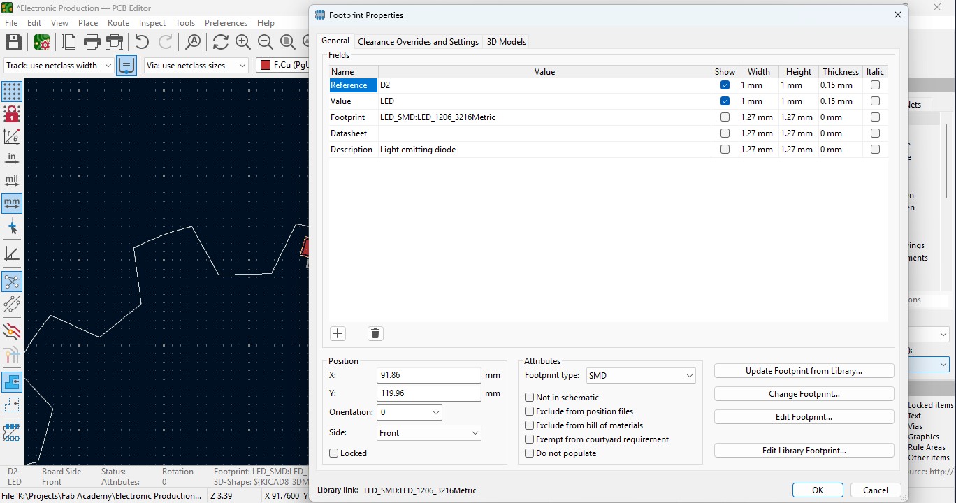
10. Click on the component and double click it and "Footprint Properties" window may appear on the orientation and change the degree to the convienent way so that adjust it on and place it.
11. Place all the Led components in the teeth of the outline as i did.
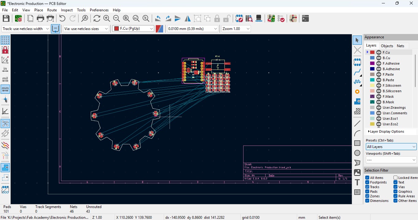
12. place all the resistor and do the same for it also as did for LED in it and rearrange it.
13. Over the right panel there are all things, click on the fourth block that is "Route Tracks" or click on "X" to start the routing.

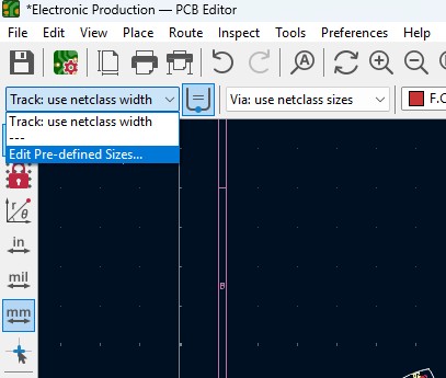
14. Over the left upper panel and click on the "Track: use netclass width" and change that to "edit pre-defined sizes" and click it.
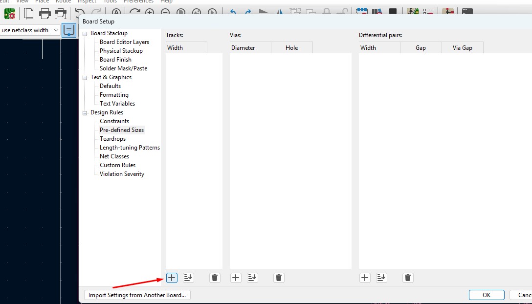
15. A new window will pop up and click on (+)icon on the Track Column "width" and click on it.
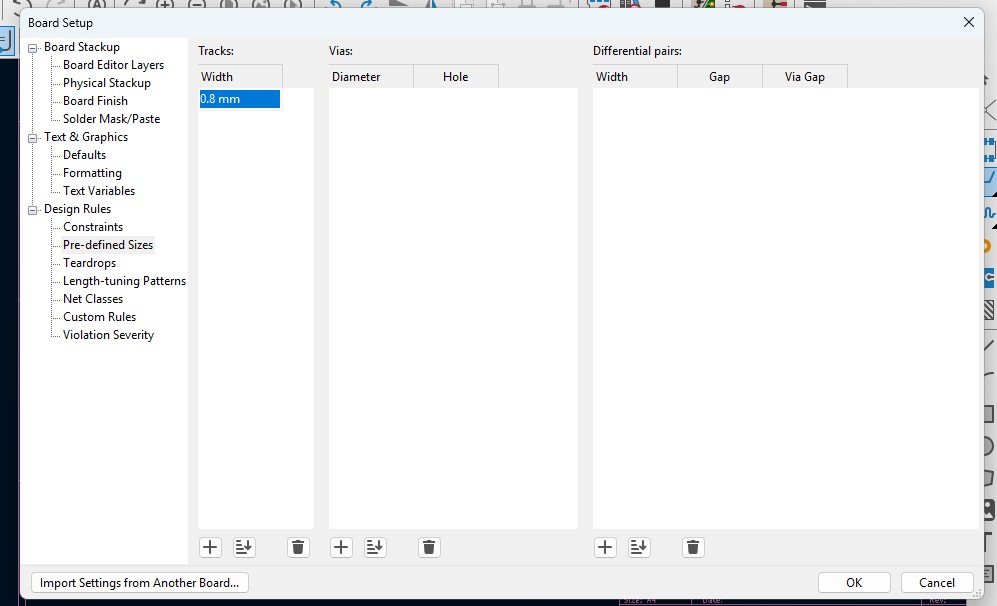
16. Change that to the your wish track size so for me i gave it to 0.8mm track width size. and click it
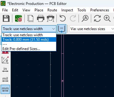
17. Now click on th esame track width in there you may see track 0.800mm width size in it. click it.
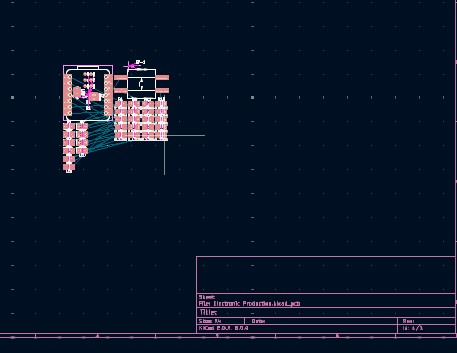
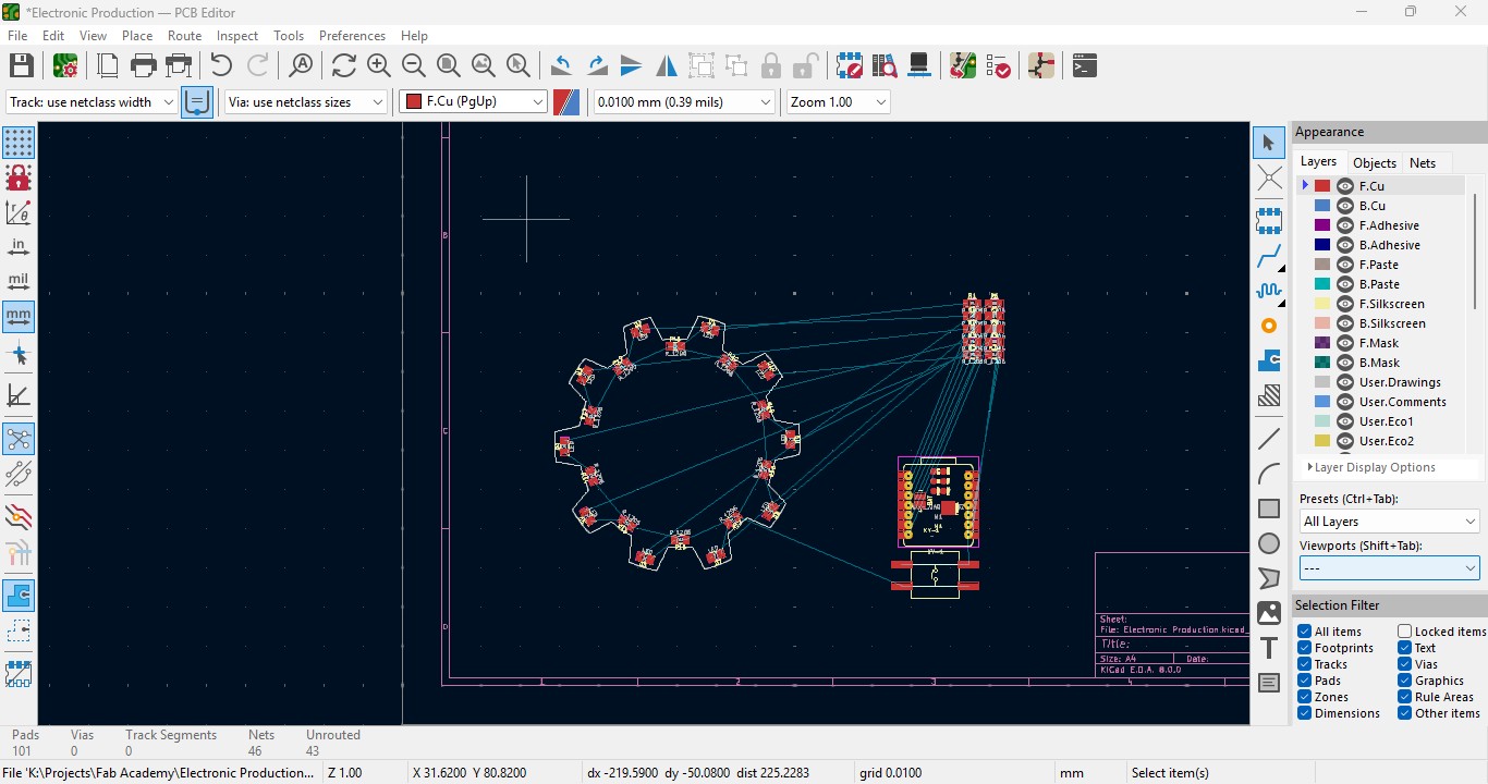
18. Place all the components in it and the design may look like this (This is my first time i made a peculiar design like this rather than greometric design)
19. Go to view -> 3D Viewer adn click it.
20. you may view the 3D design of the model we made it in PCB design.
21. Now go back and go to File -> plot and click on it.
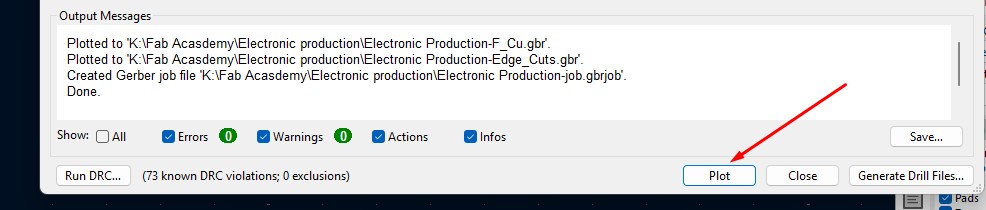
22. click on the layers that you may need in my case i need F.cu and edge cuts layers on it and click on teh output directory and change the directory on it.
23. click on the "Plot" button and the file has been generated.
Download Files
Here, you can download the files that i made over this assignment
Laser Cutter Machine
1. Cog Wheel design
2. Kicad Project file
2. Gerber files
Click here to download KiCAD
9. Now, come back to the same main window of the KiCad and go to Perferences-> Manage Footprint libraries.
10. there will be a window similar to symbol editor but in this we are gonna add footprint datas into it. go to Add (+) button and Click on it. write a Name that is Nickmake(which should be the same name that is already been allocated in symbol editor while add new symbol).
11. Navigate through and get the extracted "Kicad-master" folder and ensure that "fab.pretty"folder has been clicked to upload that into the footprint editor.
12. After the important that file you amy get to know that it has been uploaded and you visibly can see.
Here is the link button below:
Or you can download manually:
Click here to got to the Library link
Creating New Project
1. Open the Kicad and main Window will pop up and go to File -> New Project
2. Browse the location and name the Project in my case i have added "electronic Production"
3. you may see the there are two files that is
- Schematic File (.sch)
- PCB Layout File (.kicad_pcb)
Idea generation of making Design
1. I though to make a design that is different from somethinga dn i need to be in circular so i searched for the many this i got an awesome idea to make a design that is CogWheel in it.
2. download a image and im gonna use Inkscape software to edit the design simailar to make it on.
3. and this is what i made from it and downloaded as a SVG file so that i can move it as a outline on my board
Making Schematic for your circuit
1. Open the Kicad and main Window will pop up abd click on the Schematic Editor
2. A new Window is pop up that is Schematic editor weher you make schematic diagrams for your circuit
3. By clicking "A" or click on the 3 option on the right panel that is "add components" to add new components. a new window will pop up
4. search of the components that you may required in it so in this assignment i wnat these components in it
Components required
- Seeed studio Xiao ESP32C3 module X 1
- SMD LED (1206) X 10
- SMD resistor 100 ohms (1206) X 10
- SMD resistor 0 ohms (1206) X 10
- KY - 004 Tactile switch X 1
So im searching the component LED in it.
5. place the components in it
6. Duplicate the contents as per your needs.
7. As you have seen that i have places all the components in it with its quantities
8. Arrange all the components as per the you convienent and i made it look like this in it
9. Give the Circuit Connection as per your need that is by clicking "w" or click on the 5 option on the right panel that is "wire" to give connections in it
10. After all the connections are given, the remaining not connected pins are needed to connect this pins that is "no connection flags" that is avaialbe on 8th block which is in on right panel.
11. after connection all that flags you may see like this connection .
12. After all connection, go to Inspect -> Electrical Rules Checker. Click on it
13. A new window will pop up and it is mainly used to check if there is any issue or not . so do that click on "Run ERC"
14. It may start to run checker and finds all the issue and error or warnings that are available in your circuit. so find all are correct are not.
15. After doing all the things, click on the "Open PCB in board editor" to import the design from schematic design to pcb design.
Making PCB design from the Schematic Diagram
1. Open the Kicad and main Window will pop up abd click on the PCB Editor
2. This Windows is used for the PCB design that you make in schematic design.
3. Over top, you make see the symbol like that, that is used to update the PCB with changes taht made in schematic. so click that.
4. A new window will appear over that click on "Update PCB " button and all the components may list out over here click on it.
5. all the components are updated in the PCB editor and as you been seen over here.
6. Click File -> Import -> Graphics and click it to import Outline of the board.
7. A New Window will pop up and over there will be a changable dropdown go o there and click that to "Edge.Cuts" and click on the folder button change the directory.
8. A new window will come over there navigate the directory to the file where the SVG file is located and clicked on it.
9. The Edge cut outline gets out over here (as i used Cog Wheel in it) place it on.
10. Click on the component and double click it and "Footprint Properties" window may appear on the orientation and change the degree to the convienent way so that adjust it on and place it.
11. Place all the Led components in the teeth of the outline as i did.
12. place all the resistor and do the same for it also as did for LED in it and rearrange it.
13. Over the right panel there are all things, click on the fourth block that is "Route Tracks" or click on "X" to start the routing.
14. Over the left upper panel and click on the "Track: use netclass width" and change that to "edit pre-defined sizes" and click it.
15. A new window will pop up and click on (+)icon on the Track Column "width" and click on it.
16. Change that to the your wish track size so for me i gave it to 0.8mm track width size. and click it
17. Now click on th esame track width in there you may see track 0.800mm width size in it. click it.
18. Place all the components in it and the design may look like this (This is my first time i made a peculiar design like this rather than greometric design)
19. Go to view -> 3D Viewer adn click it.
20. you may view the 3D design of the model we made it in PCB design.
21. Now go back and go to File -> plot and click on it.
22. click on the layers that you may need in my case i need F.cu and edge cuts layers on it and click on teh output directory and change the directory on it.
23. click on the "Plot" button and the file has been generated.
Download Files
Here, you can download the files that i made over this assignment
Laser Cutter Machine
1. Cog Wheel design
2. Kicad Project file
2. Gerber files
Click here to got to the Library link
- Schematic File (.sch)
- PCB Layout File (.kicad_pcb)
Components required
- Seeed studio Xiao ESP32C3 module X 1
- SMD LED (1206) X 10
- SMD resistor 100 ohms (1206) X 10
- SMD resistor 0 ohms (1206) X 10
- KY - 004 Tactile switch X 1
9. Give the Circuit Connection as per your need that is by clicking "w" or click on the 5 option on the right panel that is "wire" to give connections in it
10. After all the connections are given, the remaining not connected pins are needed to connect this pins that is "no connection flags" that is avaialbe on 8th block which is in on right panel.
11. after connection all that flags you may see like this connection .
12. After all connection, go to Inspect -> Electrical Rules Checker. Click on it
13. A new window will pop up and it is mainly used to check if there is any issue or not . so do that click on "Run ERC"
14. It may start to run checker and finds all the issue and error or warnings that are available in your circuit. so find all are correct are not.
15. After doing all the things, click on the "Open PCB in board editor" to import the design from schematic design to pcb design.
Making PCB design from the Schematic Diagram
1. Open the Kicad and main Window will pop up abd click on the PCB Editor
2. This Windows is used for the PCB design that you make in schematic design.
3. Over top, you make see the symbol like that, that is used to update the PCB with changes taht made in schematic. so click that.
4. A new window will appear over that click on "Update PCB " button and all the components may list out over here click on it.
5. all the components are updated in the PCB editor and as you been seen over here.
6. Click File -> Import -> Graphics and click it to import Outline of the board.
7. A New Window will pop up and over there will be a changable dropdown go o there and click that to "Edge.Cuts" and click on the folder button change the directory.
8. A new window will come over there navigate the directory to the file where the SVG file is located and clicked on it.
9. The Edge cut outline gets out over here (as i used Cog Wheel in it) place it on.
10. Click on the component and double click it and "Footprint Properties" window may appear on the orientation and change the degree to the convienent way so that adjust it on and place it.
11. Place all the Led components in the teeth of the outline as i did.
12. place all the resistor and do the same for it also as did for LED in it and rearrange it.
13. Over the right panel there are all things, click on the fourth block that is "Route Tracks" or click on "X" to start the routing.
14. Over the left upper panel and click on the "Track: use netclass width" and change that to "edit pre-defined sizes" and click it.
15. A new window will pop up and click on (+)icon on the Track Column "width" and click on it.
16. Change that to the your wish track size so for me i gave it to 0.8mm track width size. and click it
17. Now click on th esame track width in there you may see track 0.800mm width size in it. click it.
18. Place all the components in it and the design may look like this (This is my first time i made a peculiar design like this rather than greometric design)
19. Go to view -> 3D Viewer adn click it.
20. you may view the 3D design of the model we made it in PCB design.
21. Now go back and go to File -> plot and click on it.
22. click on the layers that you may need in my case i need F.cu and edge cuts layers on it and click on teh output directory and change the directory on it.
23. click on the "Plot" button and the file has been generated.
Download Files
Here, you can download the files that i made over this assignment
Laser Cutter Machine
1. Cog Wheel design
2. Kicad Project file
2. Gerber files
9. The Edge cut outline gets out over here (as i used Cog Wheel in it) place it on.
10. Click on the component and double click it and "Footprint Properties" window may appear on the orientation and change the degree to the convienent way so that adjust it on and place it.
11. Place all the Led components in the teeth of the outline as i did.
12. place all the resistor and do the same for it also as did for LED in it and rearrange it.
13. Over the right panel there are all things, click on the fourth block that is "Route Tracks" or click on "X" to start the routing.
14. Over the left upper panel and click on the "Track: use netclass width" and change that to "edit pre-defined sizes" and click it.
15. A new window will pop up and click on (+)icon on the Track Column "width" and click on it.
16. Change that to the your wish track size so for me i gave it to 0.8mm track width size. and click it
17. Now click on th esame track width in there you may see track 0.800mm width size in it. click it.
18. Place all the components in it and the design may look like this (This is my first time i made a peculiar design like this rather than greometric design)
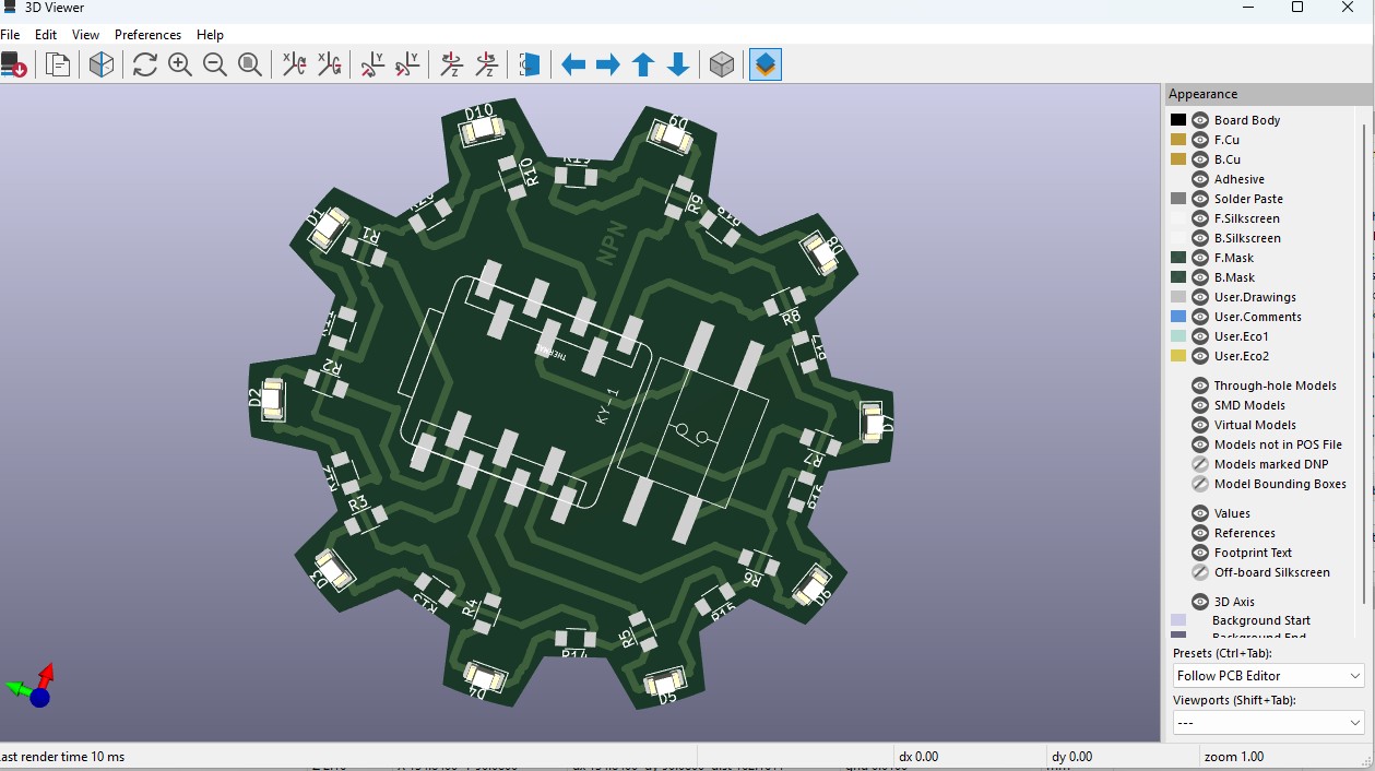
19. Go to view -> 3D Viewer adn click it.
20. you may view the 3D design of the model we made it in PCB design.
21. Now go back and go to File -> plot and click on it.
22. click on the layers that you may need in my case i need F.cu and edge cuts layers on it and click on teh output directory and change the directory on it.
23. click on the "Plot" button and the file has been generated.
Download Files
Here, you can download the files that i made over this assignment
Laser Cutter Machine
1. Cog Wheel design
2. Kicad Project file
2. Gerber files
11. Place all the Led components in the teeth of the outline as i did.
12. place all the resistor and do the same for it also as did for LED in it and rearrange it.
13. Over the right panel there are all things, click on the fourth block that is "Route Tracks" or click on "X" to start the routing.
14. Over the left upper panel and click on the "Track: use netclass width" and change that to "edit pre-defined sizes" and click it.
15. A new window will pop up and click on (+)icon on the Track Column "width" and click on it.
16. Change that to the your wish track size so for me i gave it to 0.8mm track width size. and click it
17. Now click on th esame track width in there you may see track 0.800mm width size in it. click it.
18. Place all the components in it and the design may look like this (This is my first time i made a peculiar design like this rather than greometric design)
19. Go to view -> 3D Viewer adn click it.
20. you may view the 3D design of the model we made it in PCB design.
21. Now go back and go to File -> plot and click on it.
22. click on the layers that you may need in my case i need F.cu and edge cuts layers on it and click on teh output directory and change the directory on it.
23. click on the "Plot" button and the file has been generated.
Download Files
Here, you can download the files that i made over this assignment
Laser Cutter Machine
1. Cog Wheel design
2. Kicad Project file
2. Gerber files
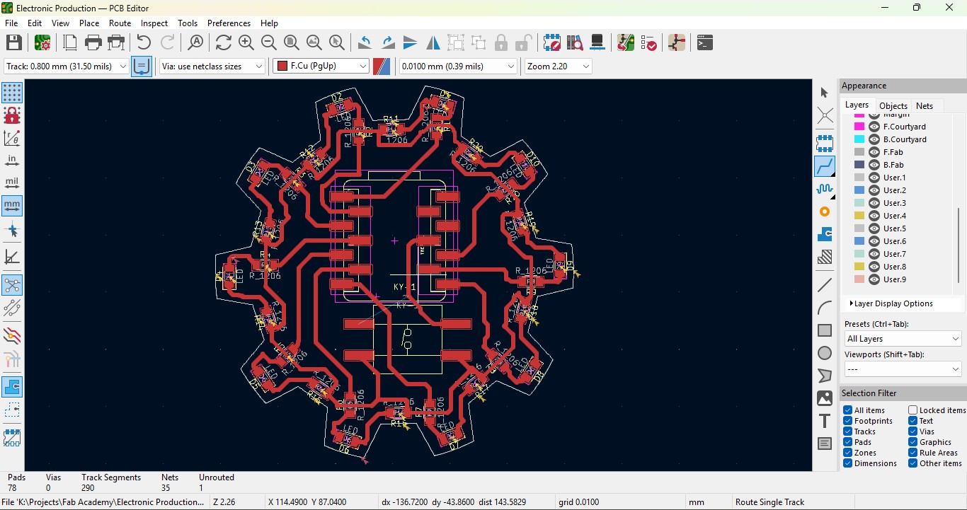
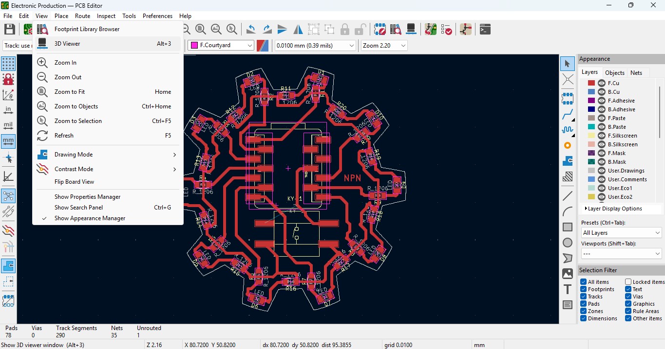
18. Place all the components in it and the design may look like this (This is my first time i made a peculiar design like this rather than greometric design)
19. Go to view -> 3D Viewer adn click it.
20. you may view the 3D design of the model we made it in PCB design.
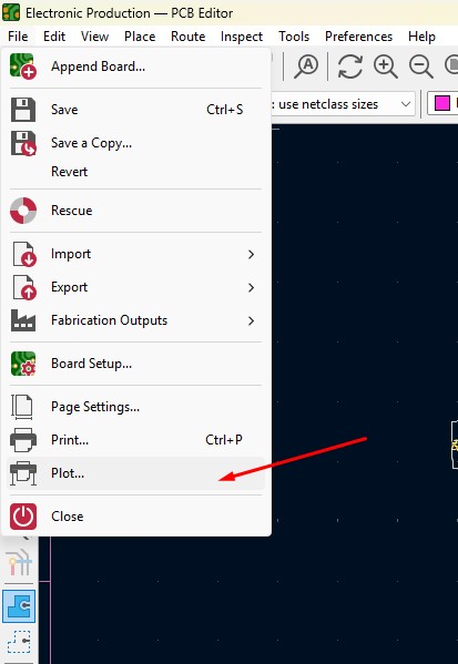
21. Now go back and go to File -> plot and click on it.
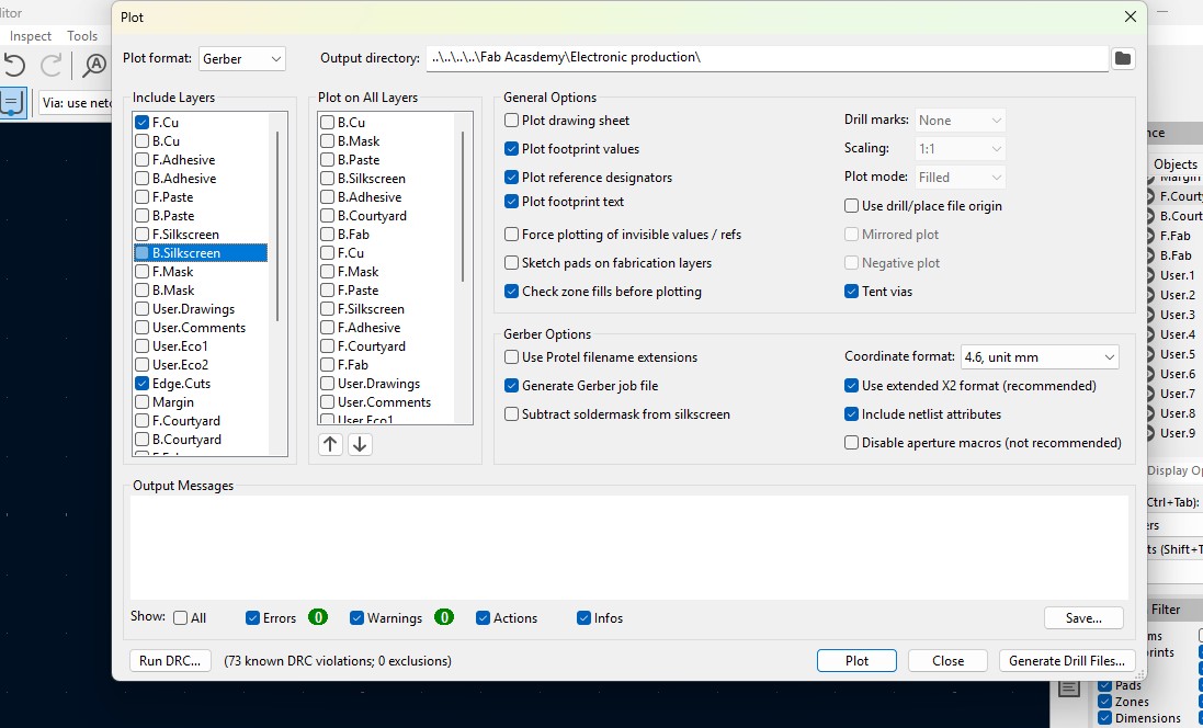
22. click on the layers that you may need in my case i need F.cu and edge cuts layers on it and click on teh output directory and change the directory on it.
23. click on the "Plot" button and the file has been generated.
Download Files
Here, you can download the files that i made over this assignment
Laser Cutter Machine
1. Cog Wheel design
2. Kicad Project file
2. Gerber files
20. you may view the 3D design of the model we made it in PCB design.
21. Now go back and go to File -> plot and click on it.
22. click on the layers that you may need in my case i need F.cu and edge cuts layers on it and click on teh output directory and change the directory on it.
23. click on the "Plot" button and the file has been generated.
Download Files
Here, you can download the files that i made over this assignment
Laser Cutter Machine
1. Cog Wheel design
2. Kicad Project file
2. Gerber files