8. Electronics Production
For the group assignment, participants will define the design rules for their in-house PCB production, detailing feeds, speeds, plunge rate, depth of cut for traces and outline, and tooling. They will also outline the workflow for sending a PCB to a board house. Documentation of their work will be shared on the group page, with personal reflections on individual pages about the lessons learned. As for the individual task, each participant will create and assess a microcontroller development board.
Assigmnent checklist
| Item | Activity | Status |
|---|---|---|
| 1 | Linked to the group assignment page. | Done |
| 2 | Documented how you made the toolpath. | Done |
| 3 | Documented how you made (milled, stuffed, soldered) the board. | Done |
| 4 | Documented that your board is functional. | Done |
| 5 | Explained any problems and how you fixed them. | Done |
| 6 | Uploaded your source code. | Done |
| 7 | Included a ‘hero shot’ of your board. | Done |
Group Assigmnents
In this assignment, we will address the following tasks:
- Characterize the design rules for your in-house PCB production process: document feeds, speeds, plunge rate, depth of cut (traces and outline) and tooling.
- Document the workflow for sending a PCB to a board house
- Document your work to the group work page and reflect on your individual page what you learned
Individual Assigmnents
In this assignment, we will address the following tasks:
- Make and test a microcontroller development board
When we are sure of the characteristics of the board, we proceed to generate the files for the CAM.
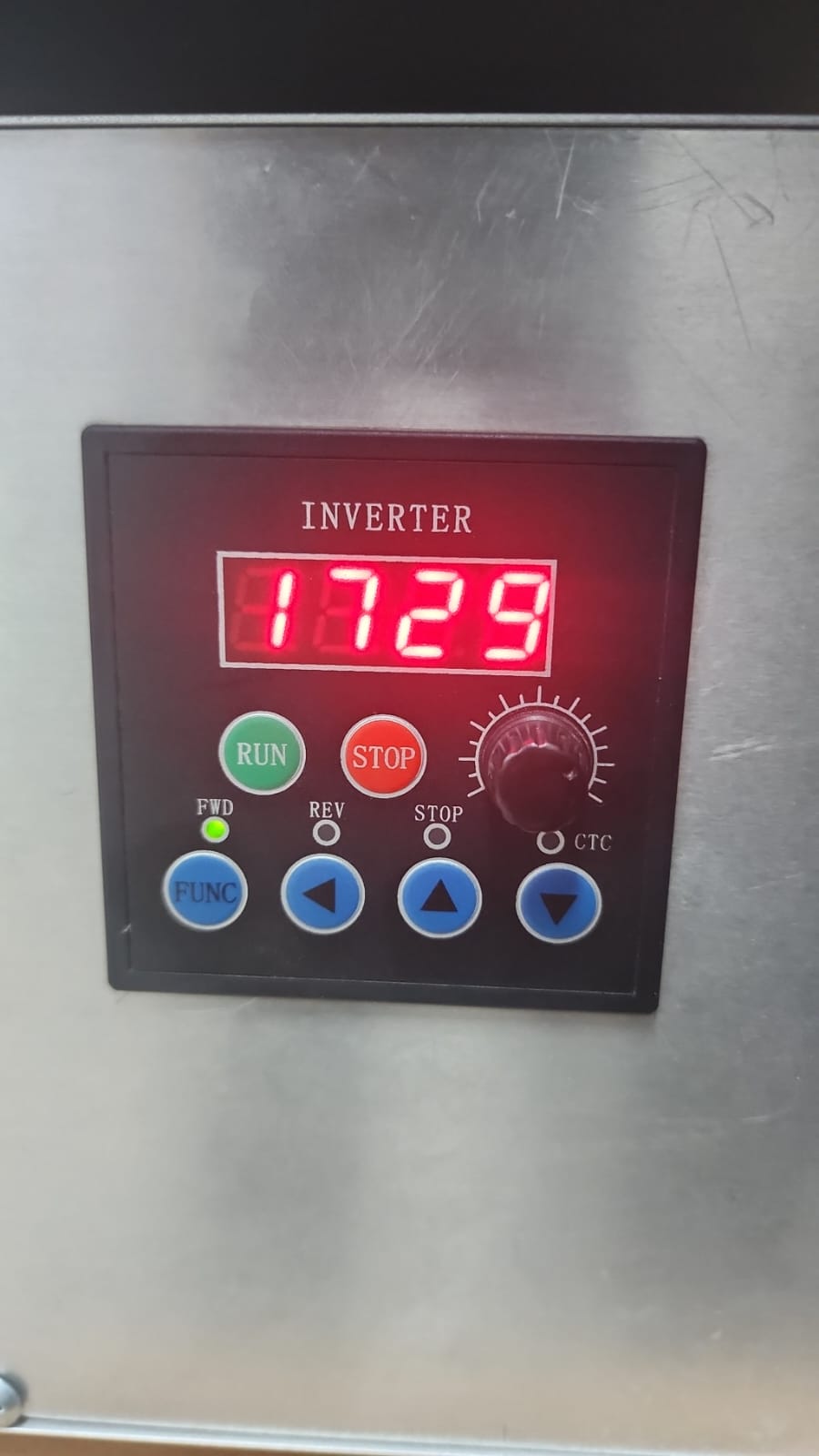
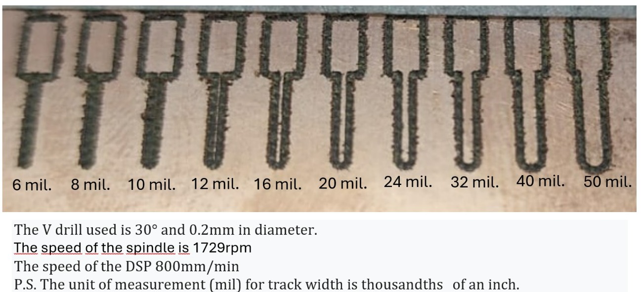
Test tracks at 1729rpm with a 30° V-bit, considering a 0.2mm diameter.
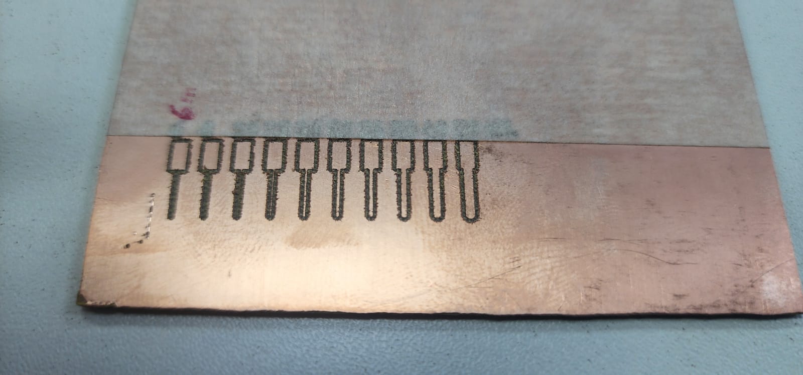
The test concludes that with the described parameters, we can isolate tracks on our CNC 6090 from a width of 20 mils (twenty thousandths of an inch) onwards. 20 mils is equal to 0.508mm. So, we can isolate tracks from a width of 0.508mm onwards.
-
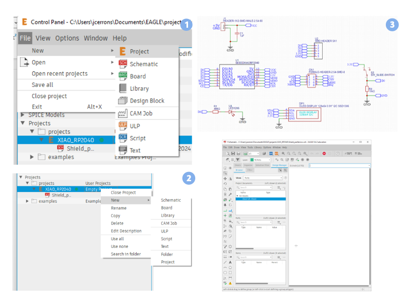
We create a new project and you can name your project according to its purpose. In this case, we will create the Shield for the XIAO_RP2040 controller.
-
In the project, we create the schematic by right-clicking.
-
Now, we design the following circuit in the Eagle Schematic environment.
 4. We select the components according to the physical list (considering their dimensions) that we have.
| Component | Reference Photo | Eagle Encapsulation | Dimensions |
|---|---|---|---|
| Header SMD Male de 1X2 pines | 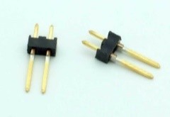 |
Created | - |
| 1X5 SMD Female Header |  |
Created | 2.54mm |
| XIAO RP2040 |  |
Created | - |
- We add the Male SMD Pinhead.
-
These components cannot be found in the Eagle library, so we need to create them manually. Let’s go to the Library. We’re going to create the schematic component using the rectangle figure to represent the component and the “pin” symbol to place the 5 pins.
-
To add the XIAO RP2040, we’ll load the following library: https://github.com/SeeedFusion/OPL_Eagle_Library. We download the compressed file and load it into the library manager.
-
In Available, we load the library and then click on Use.

- We add components and look for the XIAO RP2040 component.
- We create the 2x4 Pin Header.
- We use “Pin” and line tools to graph the symbol, in addition to plancing the name with the “95 Names” layer.
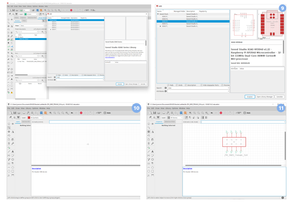
- Now we save our schematic.
- We click on Footprint and we give a name.
- We add a description in the command and accept.
- To plot the surface mount pads we click on Each thousand means one thousandth of an inch, that is, if our pins are 2.54 mm apart, then it is approximately 100 thousand, as seen in the figure.

- Pins are named by selecting them.
- With the Tplace layer we place the encapsulation.
- With the trames layer we place the name of the component.
- Now we create the device.

- We load the created symbol.
- Now we add

- Click on accept
- We click on connect, associate each footprint pin with the symbology and click accept.
- And we create a library.
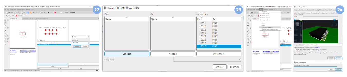
- Click to accept the location where the library will be saved.
- Now we add our creation to the schematic in the update library.
- We do the same for the 1x4 connector Once all the SMD components have been designed, we proceed to connect with the NET tool and Find each component created with the “ADD” tool PART The schematic was as follows.

- For a better understanding of the schematic and to avoid overlapping lines that can To generate confusion we use labels generated with the “LABEL” tool where in each pin that we want to connect we only extend a NET connection from the component or node and once selected in the command bar we write “LABEL” we click on the green line and a label like this example where we can Rename it with the common label shared by the components that we want to join:
- PCB BOARD Design Our card looked like this:
-
Generation of Gerbers files. Before generating the files, it is recommended that you print the circuit on paper to verify the dimensions of the components, the width of the tracks, for this you need to filter the layers with the following tool “LayerSetting” located in the upper left part of the main window of the BOARD. By clicking on the make visible icon you can filter the board to print it if what you want is to see: distribution of components, top tracks, tracks bottom, among others. In our case we only want to see the SMD pads and the tracks, we will filter the names of the components like this.
-
Now I cant print it on A4 to check the size of the tracks and pads SMD for that we click on “print”

-
When we are sure of the characteristics of the board, we proceed to generate the files for the CAM. To generate the Gerber we click on “Manufacturing”.
-
Click on CAM and select GERBER.
-
By clicking on “Process Job” we create a CAM folder.
-
And when we oppened the folder another folder “CAMOutputs” was generated.
-
Inside this we have the files:
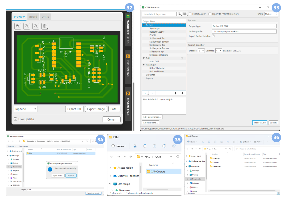
-
And the one that interests us for the next chapter is “GerberFiles”
-
Something Additional: When machining the insulation of the tracks, it is something that can take time. We recommend doing the following process: select the tool “Polygon” and draw a frame around the entire circuit as shown.
-
Ensure the insulation (Isolate) at 40 thousandths of an inch and space (Spacing) of 100 thousandths of an inch as seen in the imageLuego hacer clic en la herramienta “Raster” will get the following track.

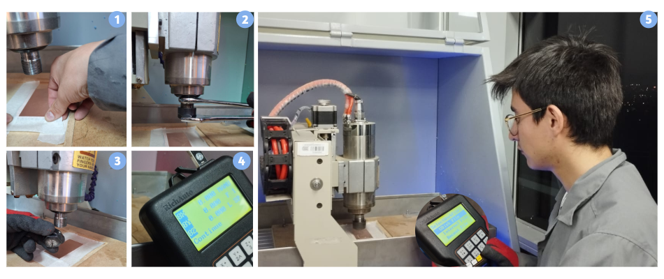
Mini CNC Router
- We secure our copper pcb board with masking tape.
- Insert our milling cutter mill big in collet and drill chuck
- Secure with our wrenches
- We choose the origin with which our machine will start to deburr.
- Select our file and click OK.
Issues, musings, and learnings.
It is very important to observe well the cutter that we use, because if the cutter is bent or the tip is damaged, the card will look bad.

• Schematic, we can make the connection diagram through symbologies. In this case, if we do not have electronic components, we can create it from the libraries as shown in this chapter. For a better visualization of the component connection plane it is necessary to use labels with the “Label” tool. • Board, we can design the tracks that will connect all the devices. It is important to have design criteria to avoid very narrow tracks or tracks that are very close together. Once this phase is completed and before manufacturing the card, verify the size of the devices with a simple paper printout. components, the width of the tracks among other characteristics. • Gerber Files, their content must be differentiated: Copper Top. CopRST Bottom, and the DRILL.