Electronics production
4.1 Group assignment | Characterize the design rules for your in-house PCB production process.
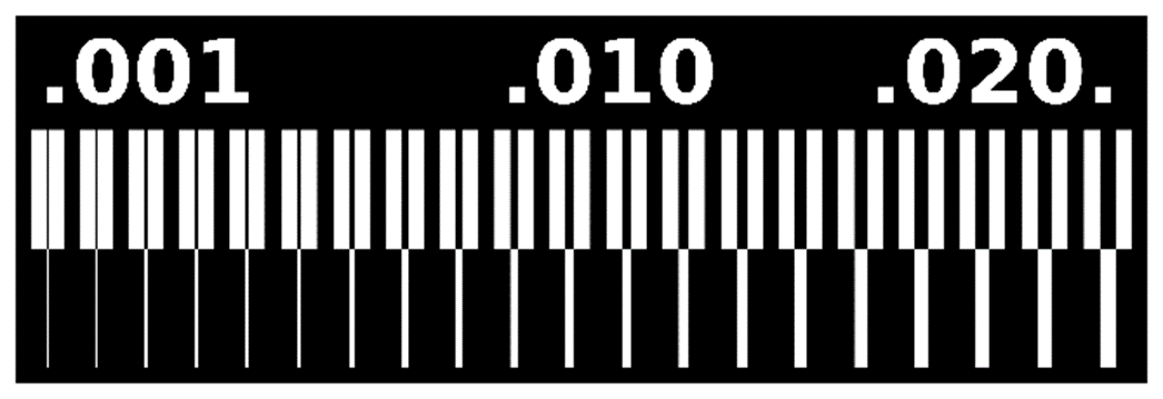
The first thing we need to do is parameterize the values to machine the piece in the image shown below, with the intention of understanding both the program language, in this case, VCarve, and the capabilities of the machine we will be using to manufacture the PCB's. The CNC router machine we will be using is a Roland SRM-20 model, which has a working area of 203.2 mm (X) × 152.4 mm (Y) × 60.5 mm (Z). This machine can work with different materials such as plastic, wood, foam, modeling wax, and laminated boards for electronic circuits.
On our laboratory webpage click here, you can find a tutorial for both: VCarve and VPanel (which we use for sending cuts). However, to complement that information, I will provide a summary of what our team did for this specific task.
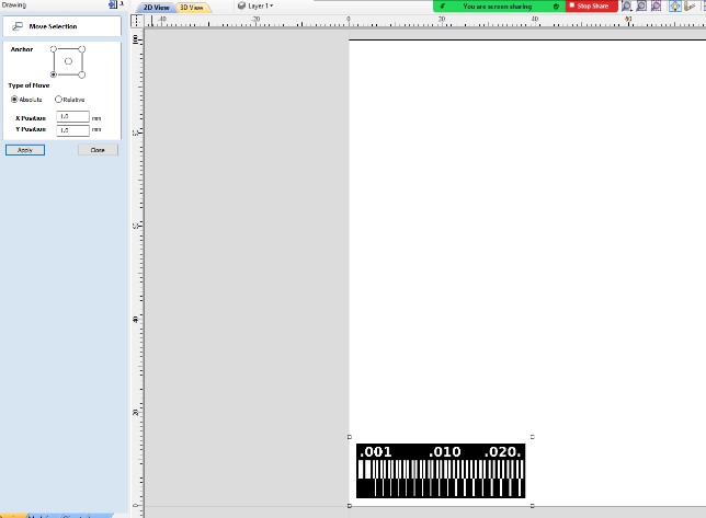
First, we downloaded the image and opened it in VCarve. It's important to position the image in the bottom left corner to avoid wasting material. Additionally, it's much easier to calibrate the router in this location, as we have better visibility the board and the drill. It's crucial to note that our VCarve is already configured with the working area, in this case is 10 x 10cm, corresponding to the size of the copper board.
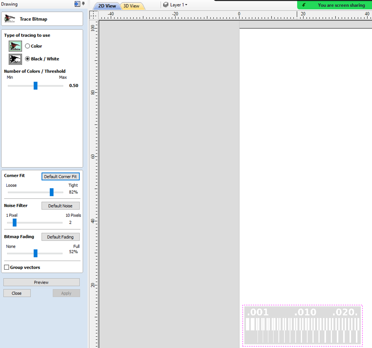
The next step is to vectorize the image by clicking on the bird icon. It is not necessary to adjust the default values since this image has only 2 colors, and both have high contrast. In this case, we just click to generate a preview, and if everything looks good, we click "Apply button" and close the window.
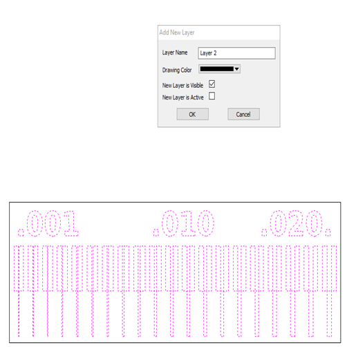
The third step is to generate two different layers: one for the traces that will only be roughed out, and another layer for the contour that will be cut. It is crucial to separate them as both will be machined with different drills.
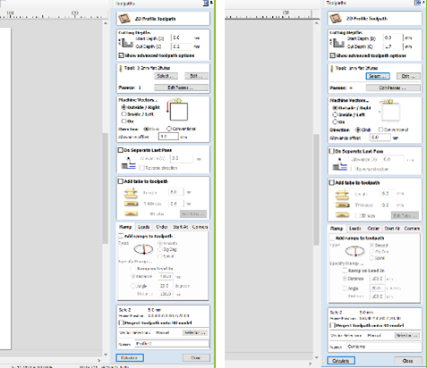
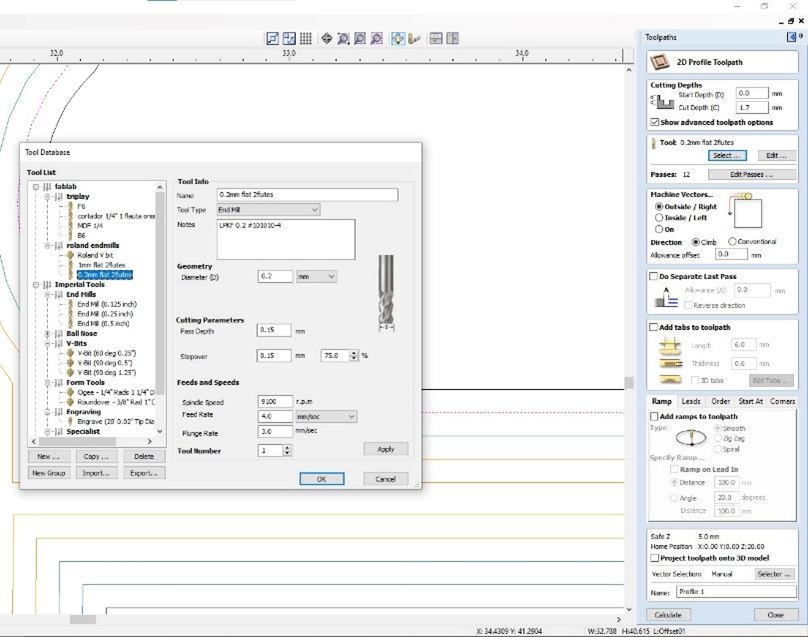
Next, we will design the toolpaths for each layer clicking on the menu located in the upper right corner. There, we will select the 1mm drill, with a cutting depth of 1.7 mm, and for the traces, we will use a 0.2mm drill with a cutting depth of 0.2mm, this will only removes the copper but will not cut the board.
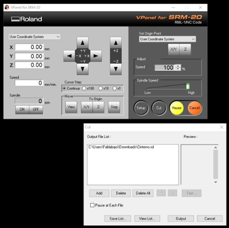
Now that we have both files ready, it's time to open each one in VPanel. We should first send the traces and, at the end, the outline file to prevent the piece from moving during the process. In the image, you can see the manipulation options; you just need to move in the x, y, and z coordinates to set the origin. This will be the place where we want the piece to be located, but as mentioned before, we will position it in the bottom right corner. Once these values are defined, we can start by clicking the resume button, and the machine will automatically begin working.
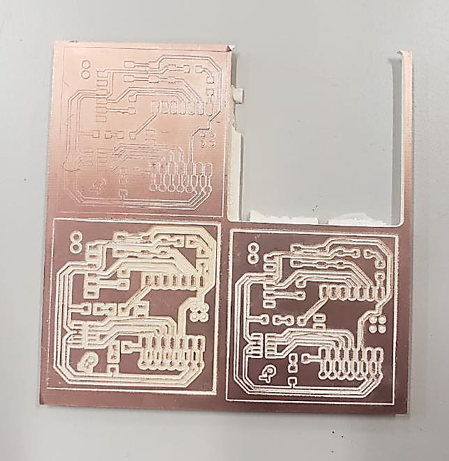
Finally, all that's left is to wait for the machine to finish its job, this will take around 10 to 15 minutes. In the image, we can see the final result.
The result of the traces was good, however, the contour result was not good at all, we assume that this is because the drill bit ran very quickly and did not have much sharpness.
4.2 Personal conclusions.
I realized that in addition to the parameterization in the software, it is crucial to choose the right drills, to also know the measurements of the material we are working on and calibrate the machine properly. Otherwise, the entire job can go wrong, leading to raw material wastage and a significant loss of work time. The programs are actually very easy to use, we just need to be extremely organized and methodical because errors can occur quite easily.
4.3 Individual | Write a program for a microcontroller development board to interact and communicate.
This is the suggested PCB that we should build from zero. Unfortunately, at the moment, in our laboratory we don't have all the components needed, and although we have already ordered them, I am not sure if they will arrive on time.
Even though, I will cut it on the Roland machine, and if the components arrive in time, I will solder them. As a plan B, I will use another PCB designed by my instructor Luis Hernandez. We have all the components for this one, so I hope this simultaneous exercise will be a success.
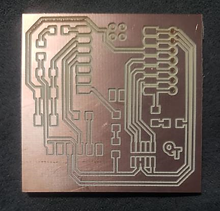
Quentorres PCB
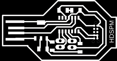
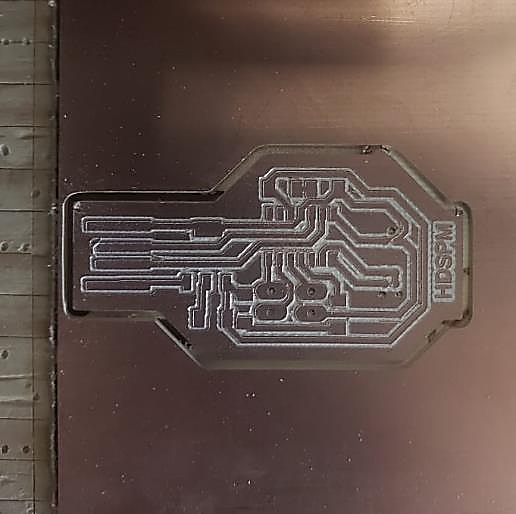
HDSPM PCB
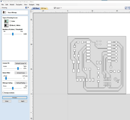
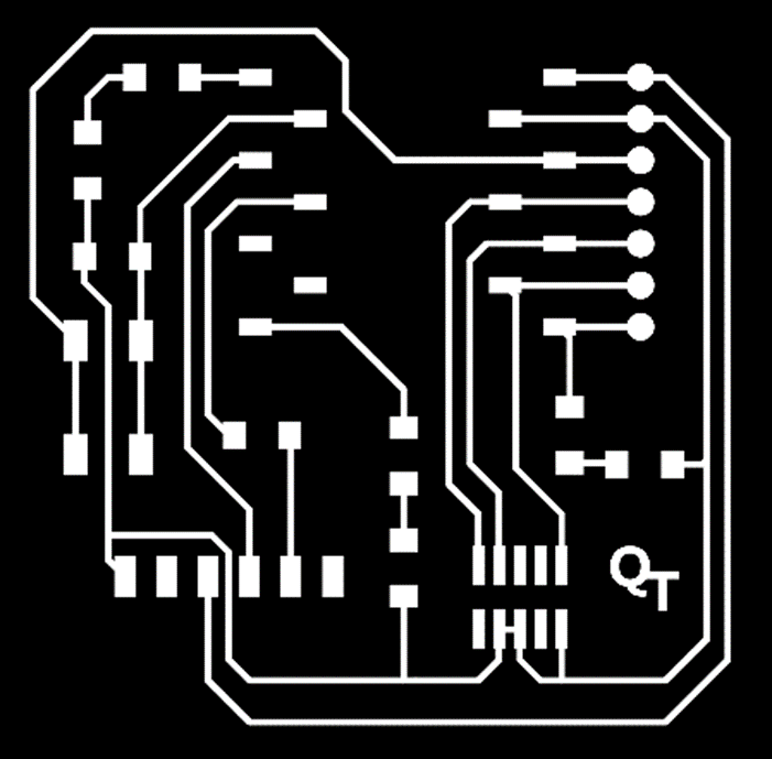
Traces Bitmap
I imported the image and placed it in the lower left corner to later be able to manipulate it better on the router
Mills
The machining process for this piece is exactly the same as the previous one; we need two drills: one for the traces and other for the contour line. However, we must be very careful with the depths and passes the drills will make since it is another drawing with very specific and different characteristics.
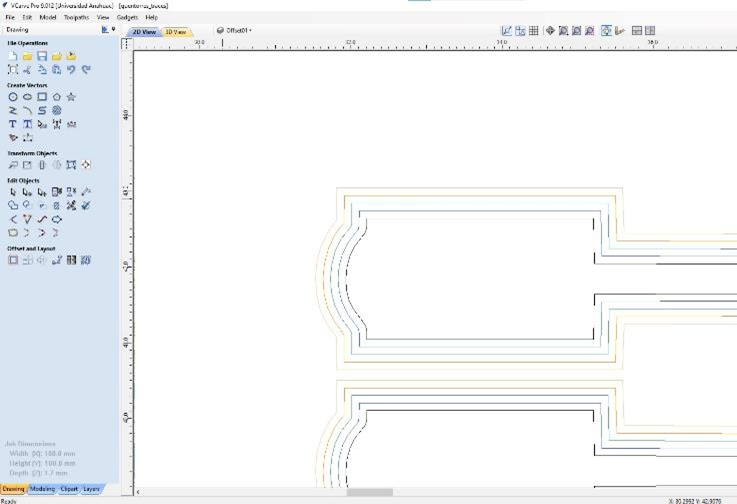
Drawing Traces
The first time I sent it to the Rolad, I followed the same criteria as the previous exercise, but added 3 traces offsets to remove more cooper around the PCB traces in order to make soldering easier. However, the time it increases was too much and the traces went very thin, so it didn't work that way. I fix it drawing just one trace offset.
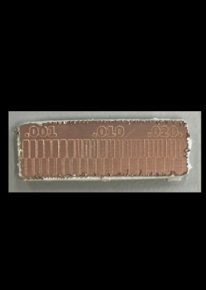
Depth error parameters
Another mistake I made was lowering the depth too much, leaving very thin PCB traces and some of them were completely broken. After several tests, the appropriate depth turned out to be 0.2 mm
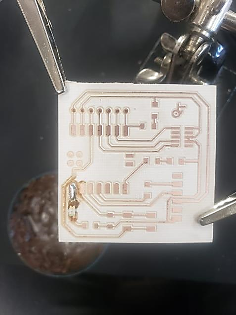
Final Quentorres PCB
In the end, it turned out well, and I have the PCB ready, waiting for all the components to arrive soon. 🫶
Final HDSPM PCB
I will also make the HDSPM PCB, following the same criteria as before and I will manually clean the copper that is not part of the traces to simplify the soldering work.
Definitely this time was easier and faster because i already learned from mistakes and analysis.
UPDATE: The componentes for the Quentorres PCB arrive on time, so I decided to continue working with it first.
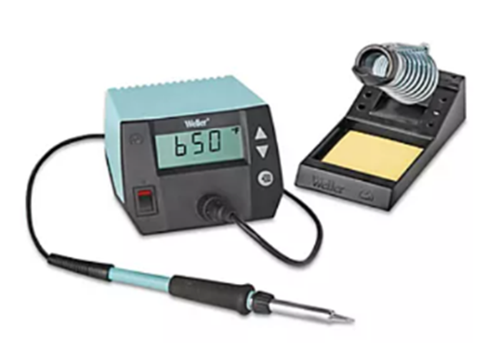
"The first thing I did after machining the board on the router was to remove with a cutter all the excess copper to facilitate soldering. Then, I started soldering all the components with a soldering iron at 300°C and tin. The one that gave me most troubles was the connector, especially because its terminals are located above the board, so I had to first put solder points on the pads and then on its terminals.
To perform the programming, I connected the board to my computer and opened Arduino IDE, following the steps in this link: steps, and the one made from my teammate Israel Santacruz: programming, who is a mechatronic engineer and is much more familiar with this. Also my instructor Luis Hernandez, explained me a bit about the programming language.
Below, I will add some images of my process and images
Soldering process
I did the soldering with a Weller statión, model H-10799. I did very well soldering most of the parts, but in the lower left part I accidentally removed a trace when removing the excess of copper and I had to make a bridge to rescue the trace to not have to print it again. To check the continuity of this and the other traces, I used a multimeter. Fortunately, everything works perfectly.
Programming.
Luis Hernández intro to programming
This is an express lesson that my instructor Luis Hernández gave me, where he explains the basic programming structure, which is divided into three parts:
1. description of variables: as its name says, it describes each of the elements arranged on the card.
2. program configuration. It is the part in charge of collecting the configuration
3. Loop section. It is the one that contains the program that is executed cyclically.
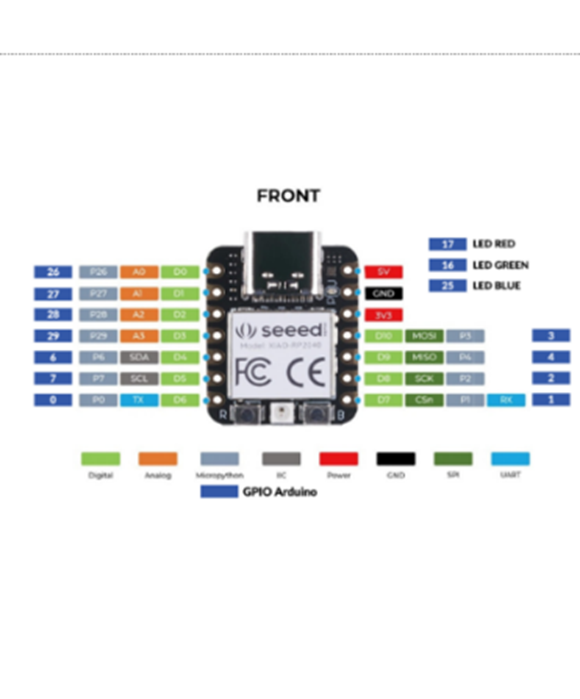
Reference image to locate LEDs possition.
I used this scheme to verify LEDS position and describe the variables properly
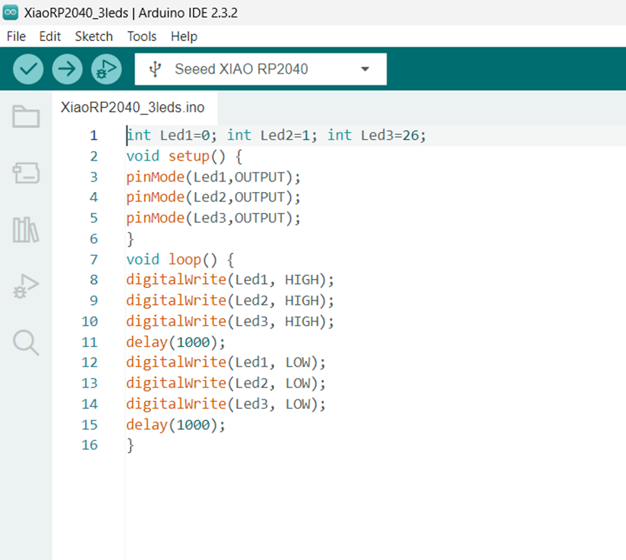
Program in Arduino IDE
int Led1=0; int Led2=1; int Led3=26;
void setup() {
pinMode(Led1,OUTPUT);
pinMode(Led2,OUTPUT);
pinMode(Led3,OUTPUT);
}
void loop() {
digitalWrite(Led1, HIGH);
digitalWrite(Led2, HIGH);
digitalWrite(Led3, HIGH);
delay(1000);
digitalWrite(Led1, LOW);
digitalWrite(Led2, LOW);
digitalWrite(Led3, LOW);
delay(1000);
}
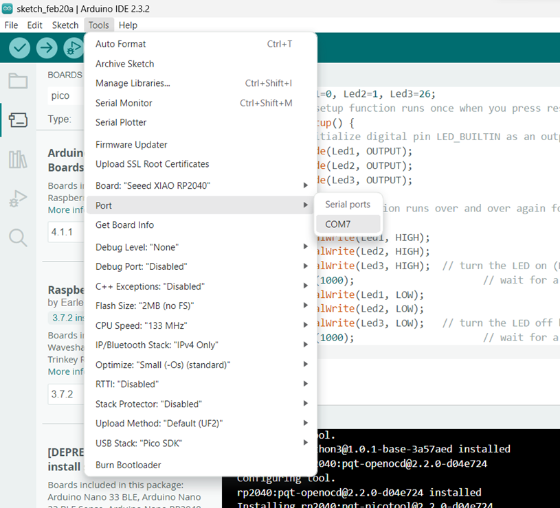
Connection of the XIAO RP2040 board
4.5 Personal conclusions
This particular task took me a lot of time to understand, not only because of the numerous processes involved, but also due to the imperfection of the results and the different samples we had to make to find the ideal parameters.
The result of the traces was good, however, the contour result was not good at all, we assume that this is because the drill bit ran very quickly and did not have much sharpness. slowing down and cutting with a newer bit could be a solution.
I have no programming background knowledge and had soldered only a couple of times before, but I am satisfied with the results because, still not being an expert, but now have a much better understanding of what I am doing and the basic criteria involved.