Week 8: Electronics Design
Group assignment:
- Use the test equipment in your lab to observe the operation of a microcontroller circuit board (as a minimum, you should demonstrate the use of a multimeter and oscilloscope)
- Document your work on the group work page and reflect what you learned on your individual page
Individual assignment:
- Use an EDA tool to design a development board to interact and communicate with an embedded microcontroller
Group assignment:
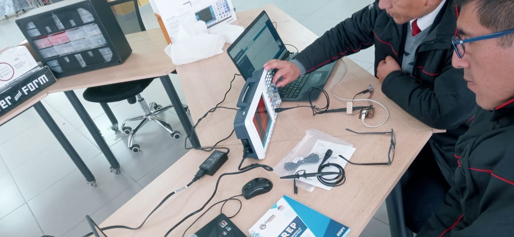
In this group work from Cerro de Pasco we met with my colleague Renso and from the city of Huánuco with our colleague Ronal via Google Meet, to be able to interact and compare the operation of the oscilloscope, which in our case is the WON SmartDS 7202.
Group Work Link
Owon SDS7202 Series SmartDS Deep Memory Digital Storage Oscilloscope with VGA Interface, 2 Channels, 60 MHz, 500 MS/s Sample Rate. Features:
- Two-channel 60 MHz digital oscilloscope, for electronic applications such as product design and debugging, repair and maintenance, and electrical engineering education
- Maximum real-time sampling rate of 250 MS/s per channel and record length of 10 Mpts per channel to acquire and process detailed waveforms
- Advanced triggers allow isolation of specific signals and a trigger hold function stabilizes triggering on complex waveforms
- Three math functions plus FFT and 20 automatic measurements to analyze waveforms
- 8” color TFT-LCD for viewing waveforms and a VGA port for connecting to an external monitor.
Digital Multimeter S-75
Features.
- Maximum voltage: 500vdc or 500vac
- Protection Fuse: 200ma/250v
- Power:9vdc
- Display:LCD.1999counts,Lighting
- Measurement method: A/D double slope integration
- Operating Environment :0°C TO 40°C
- Battery indicator: appears on the screen
- Measurements: 31.5mm x 91mm x 189mm
- Weight:approx.280g
Tests with the Oscilloscope
 Teamwork using oscilloscope.
 Preparing the equipment to launch.
 Pressing the power button.
 Connecting the tips of the oscilloscope to the ground and signal terminals of the board
 Setting the signal amplitude button
 Viewing the signal on the oscilloscope on channel 1 when the potentiometer is at its low value
 Increasing the value of the potentiometer by half
 When the potentiometer is increased to the maximum value.
 Shows when the signal is expanded
 Configuring so that the signal is cleaner with a low potentiometer.
 Configuring so that the signal is cleaner with a high potentiometer
 Finishing performing the oscilloscope analysis
Tests with the Multimeter
 Measuring the five volt power entering the potentiometer.
 Measuring the output of the potentiometer when it is raised to ten percent of its value
 This is what it measured when the potentiometer value was raised to eighty percent.
Conclusions
We learned that it is important to perform a calibration using the equipment’s own output values or oscilloscope signals. Our initial mistake was not understanding why the sensor values were so high and seemed incorrect. However, by realizing the importance of testing with the equipment’s own output first, we were able to obtain more accurate and realistic values.
Individual assignment:
- Use an EDA tool to design a development board to interact and communicate with an embedded microcontroller
To create a board we use the Kicad 8.0 software. Once created we will connect with the ESP32 C3 Microcontroller.
STEP 1: We enter the following address to download the kiCad 8.0 software: https://github.com/KiCad/kicad-source-mirror/releases/download/8.0.0/kicad-8.0.0-x86_64.exe
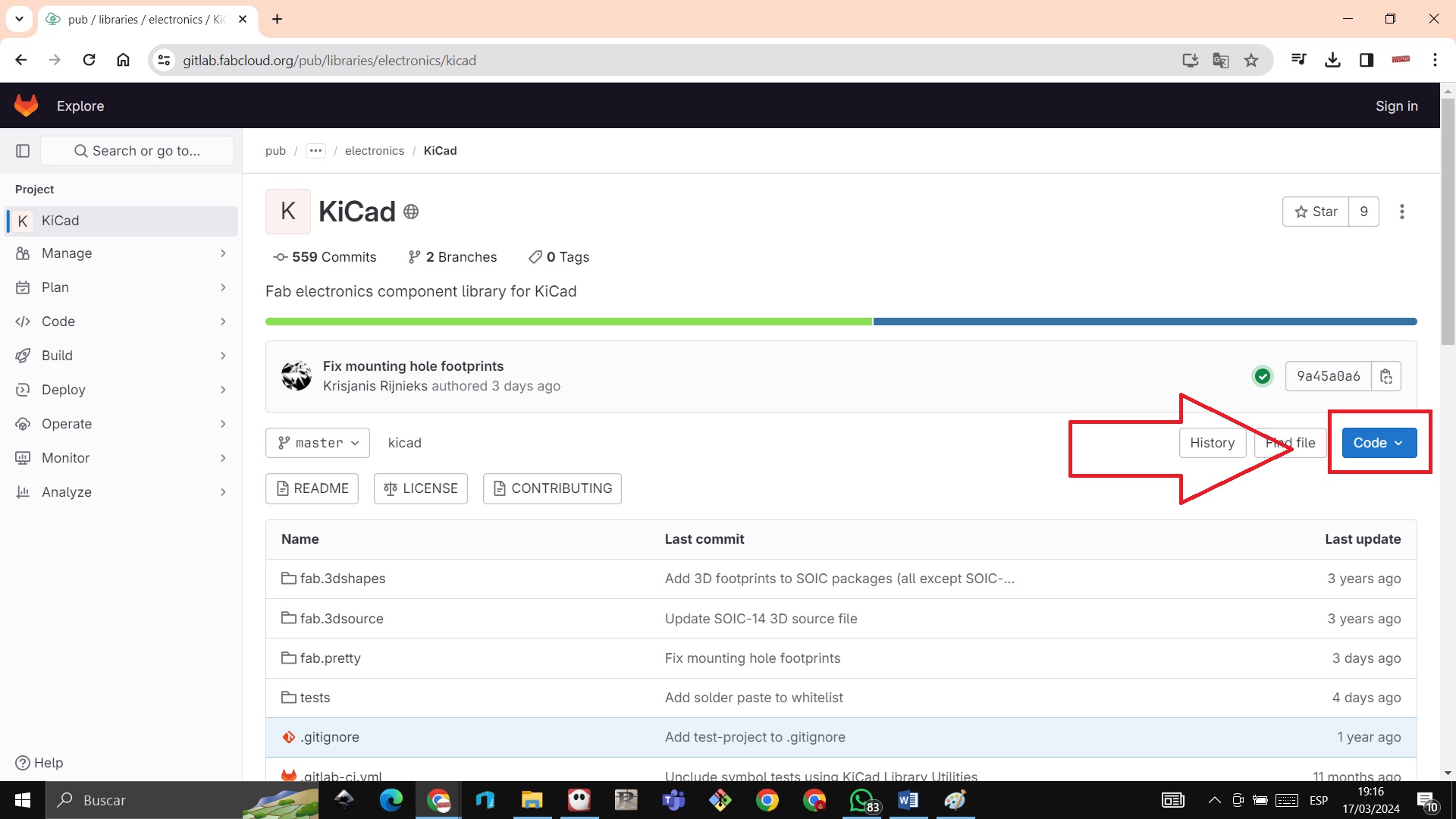
STEP 2: We enter the kiCad 8.0 library in Git Lab and download it in code and then in zip
https://gitlab.fabcloud.org/pub/libraries/electronics/kicad
 STEP 3: We open kiCad 8.0 / file / new project
 STEP 4: We write the name of our sensor1 project and save it in a folder
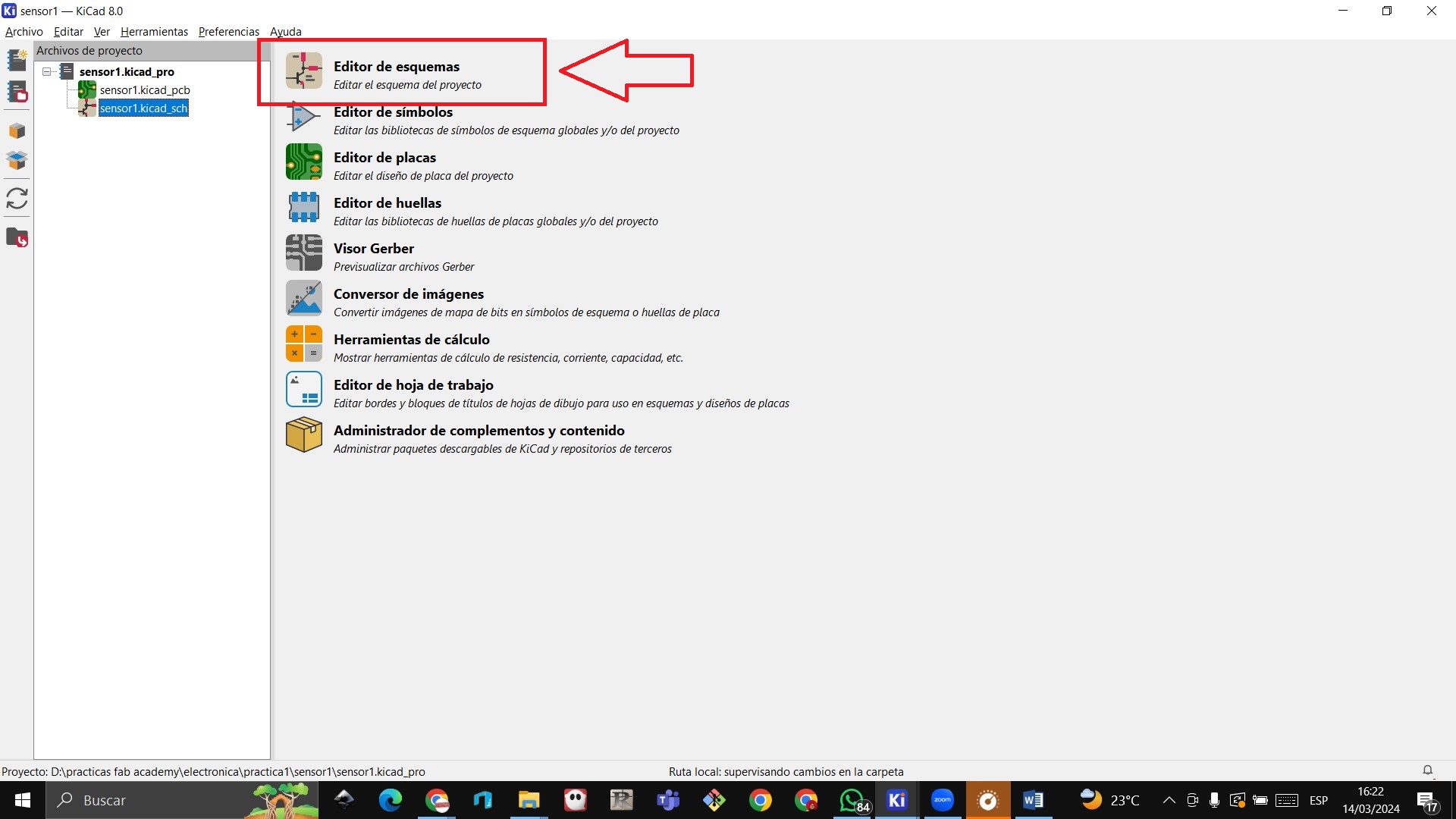
 STEP 5: We write the name of our sensor1 project and save it in a folder and the following window will appear, then we click on the schematic editor
 STEP 6: We click on the symbol editor to add the libraries
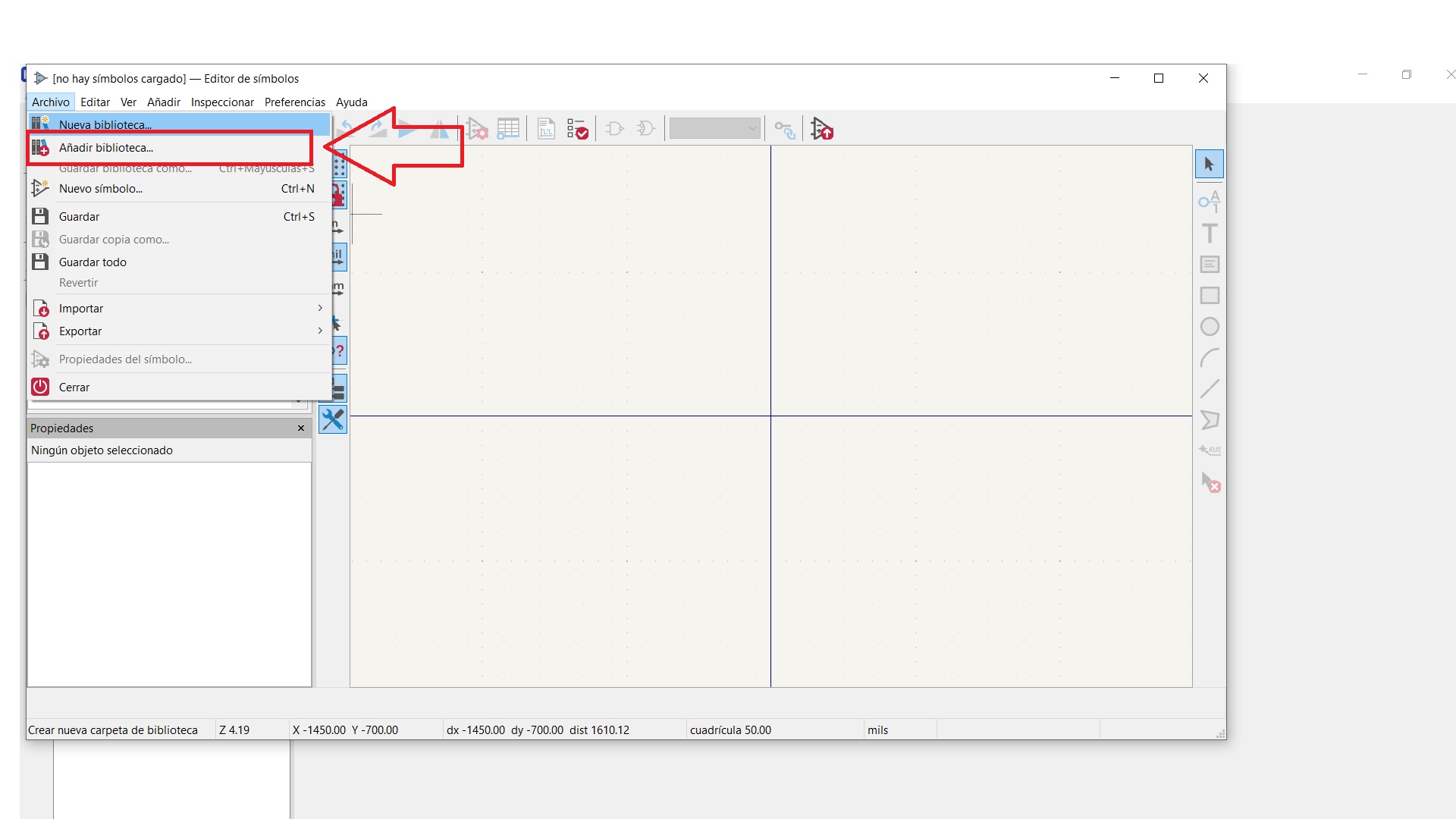
 STEP 7: We go to file add library
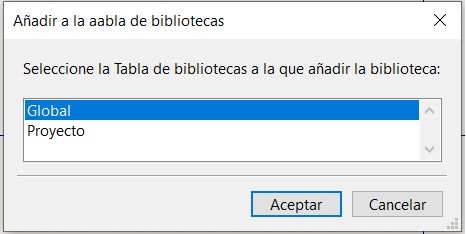
 STEP 8: We choose global to add to all other projects.
 STEP 9: We select the kicad-master folder and locate the fab.kicad_sym file
 STEP 10: We verify that it already pulls the fab folder and we close
 STEP 11: We open the schematic editor, we are going to add symbols and then we choose the XIAO-ESP32C3 symbol and click accept

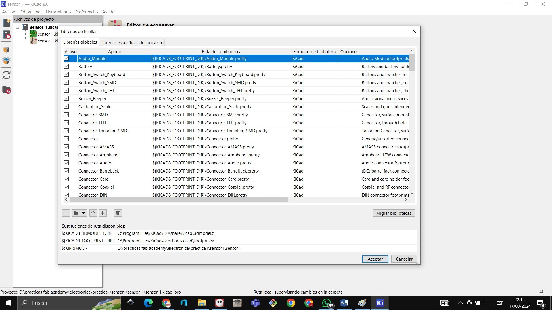
 STEP 12: We manage the fingerprint library in the main /preferences/manage fingerprint library

 STEP 13: We create the fab folder and look for the Fab.pretty folder to add the libraries
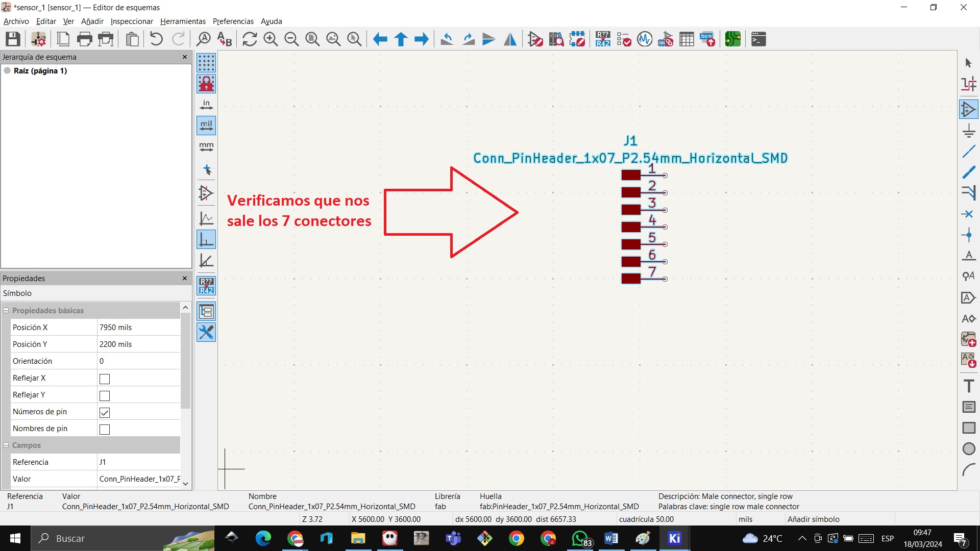
 STEP 14: Now if we start designing our card, for which we go to the schematic editor, in adding symbols we go to the fab folder and look for them to have 7 connectors
 STEP 15: We verify that it comes out in the following way and the idea is to create the board to connect to the quentorres
 STEP 16: We orient ourselves from the image to create our plate
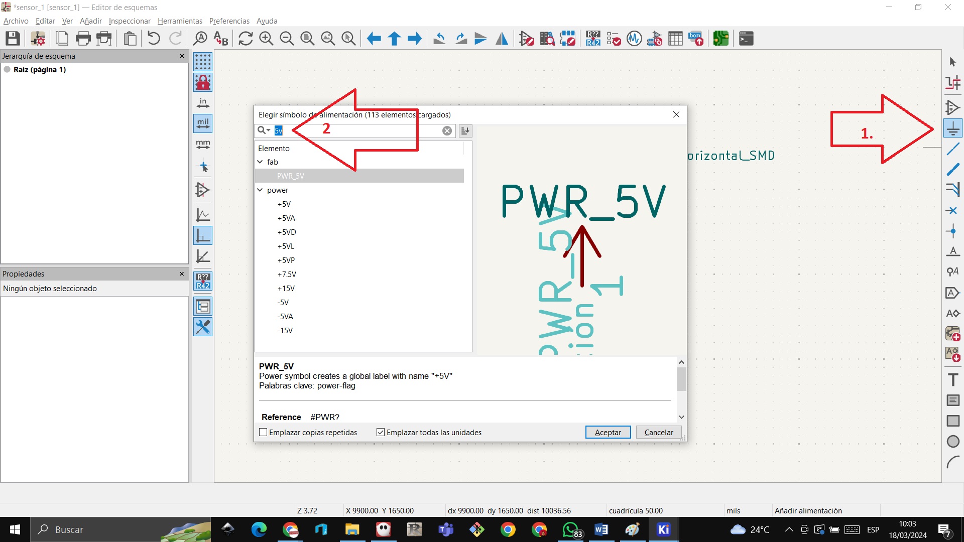
 STEP 17: We are going to add power symbols and look for PWR_5V by writing 5V
 STEP 18: We locate the 5V with the mouse
 STEP 19: We do the same procedure with 3v

 STEP 20: We enter the preferred GND of the fab folder, to rotate we select the symbol and press the letter R so that it can rotate and the letter G to move

 STEP 21: We click on ESC to exit any tool and then with the mouse pointer we join the tracks
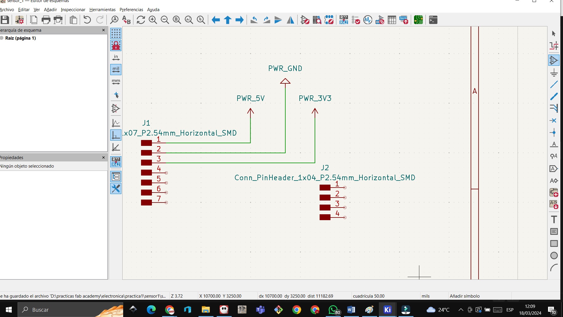
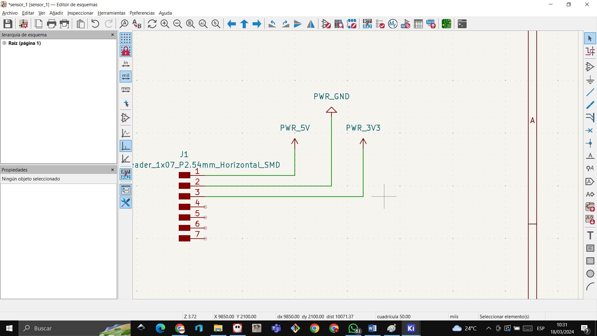 STEP 22: Now we define that we are going to connect a proximity sensor
 STEP 23: We now add 4 connectors for which we go to add symbols / the fab folder / and look for the 4 connectors
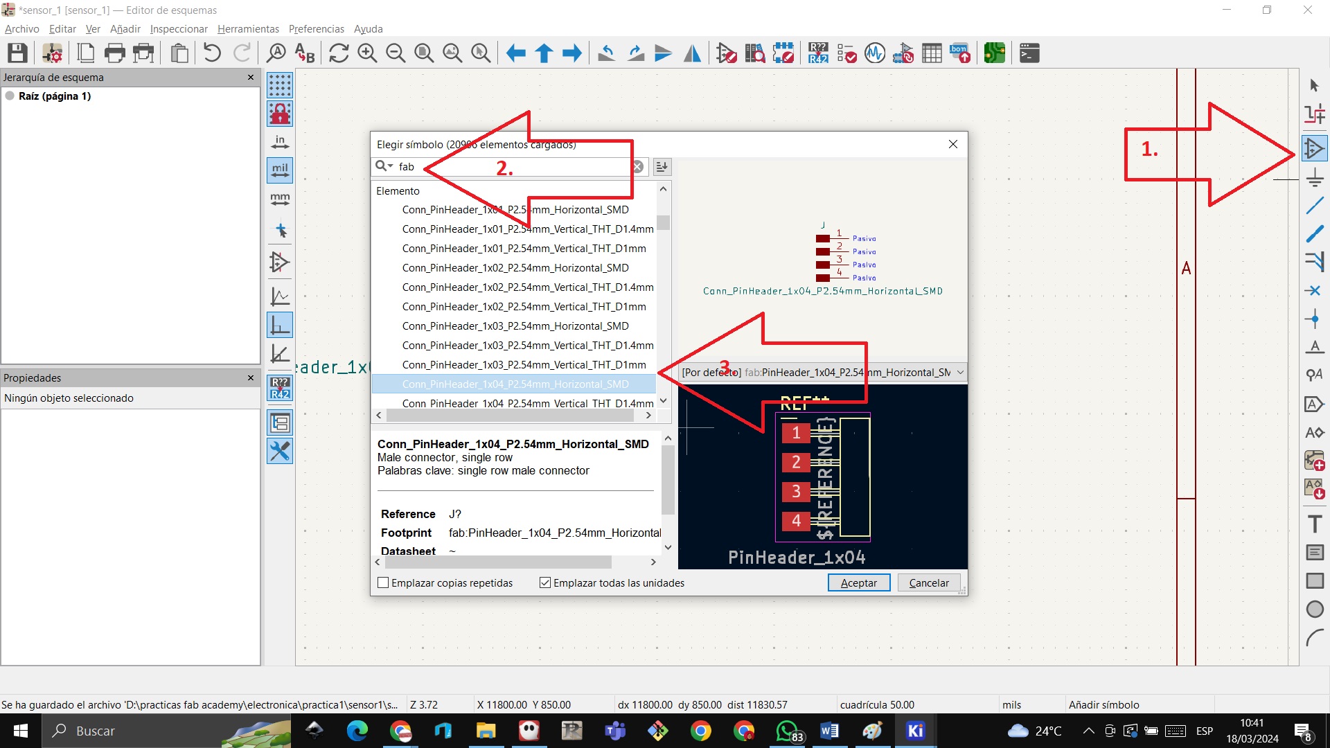
 STEP 24: We mirror the 4-connector symbol
 STEP 25: Select the 5v symbol then CTRL + D to duplicate and move and then connect
 STEP 26: We add components, a switch and a resistor


 STEP 27: We add a 3v and GND
 STEP 28: We connect the 3V, the switch and the GND
 STEP 29: We enter a 1206 led and duplicate the GND with CTRL + D
 STEP 30: When it is joined it looks like this and we join it to pin 7
 STEP 31: We click on verify fingerprints and we get that everyone has fingerprints
 STEP 32: We update the schematic plate and if we see that there are no errors we update

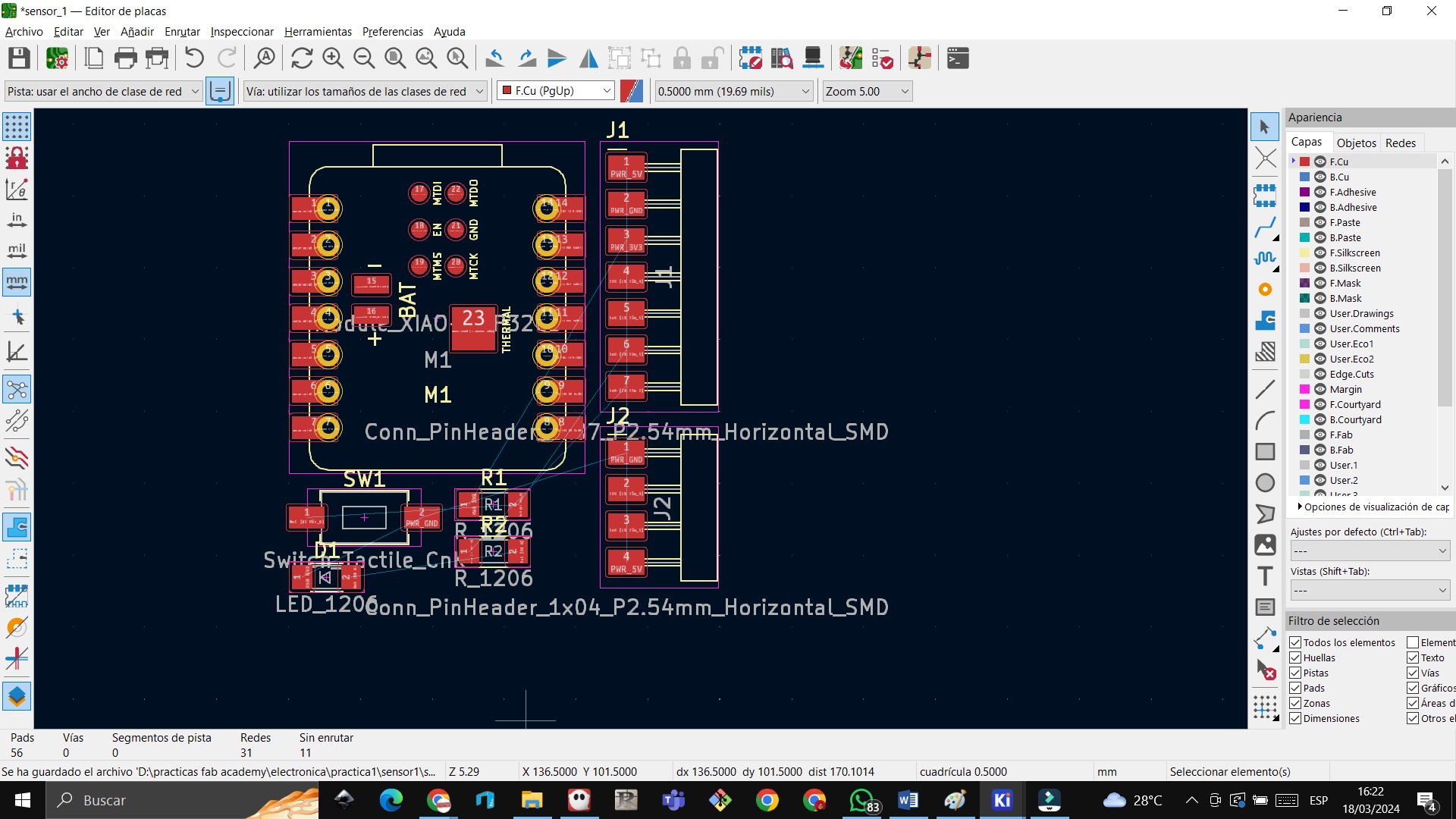
 STEP 33: In the schematic we see the xiao esp 32 and our board that we are working on
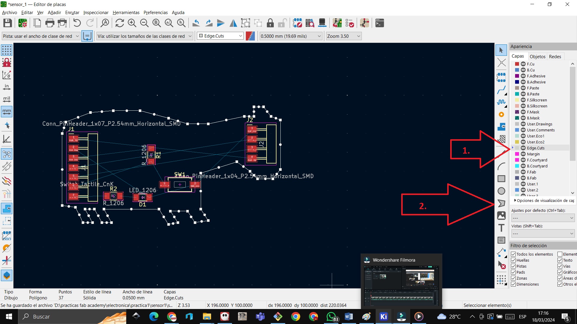
 STEP 34: We enter Edge Cuts and then draw a graphic polygon
 STEP 35: We click on the screen to show 3D viewer and we see that a moving image appears when we move the mouse

 STEP 36: To design the width of the tracks we are going to edit defined sizes
 STEP 37: The following window appears and in the + sign we add the thicknesses of the tracks, 1.2mm is recommended since current passes through that track
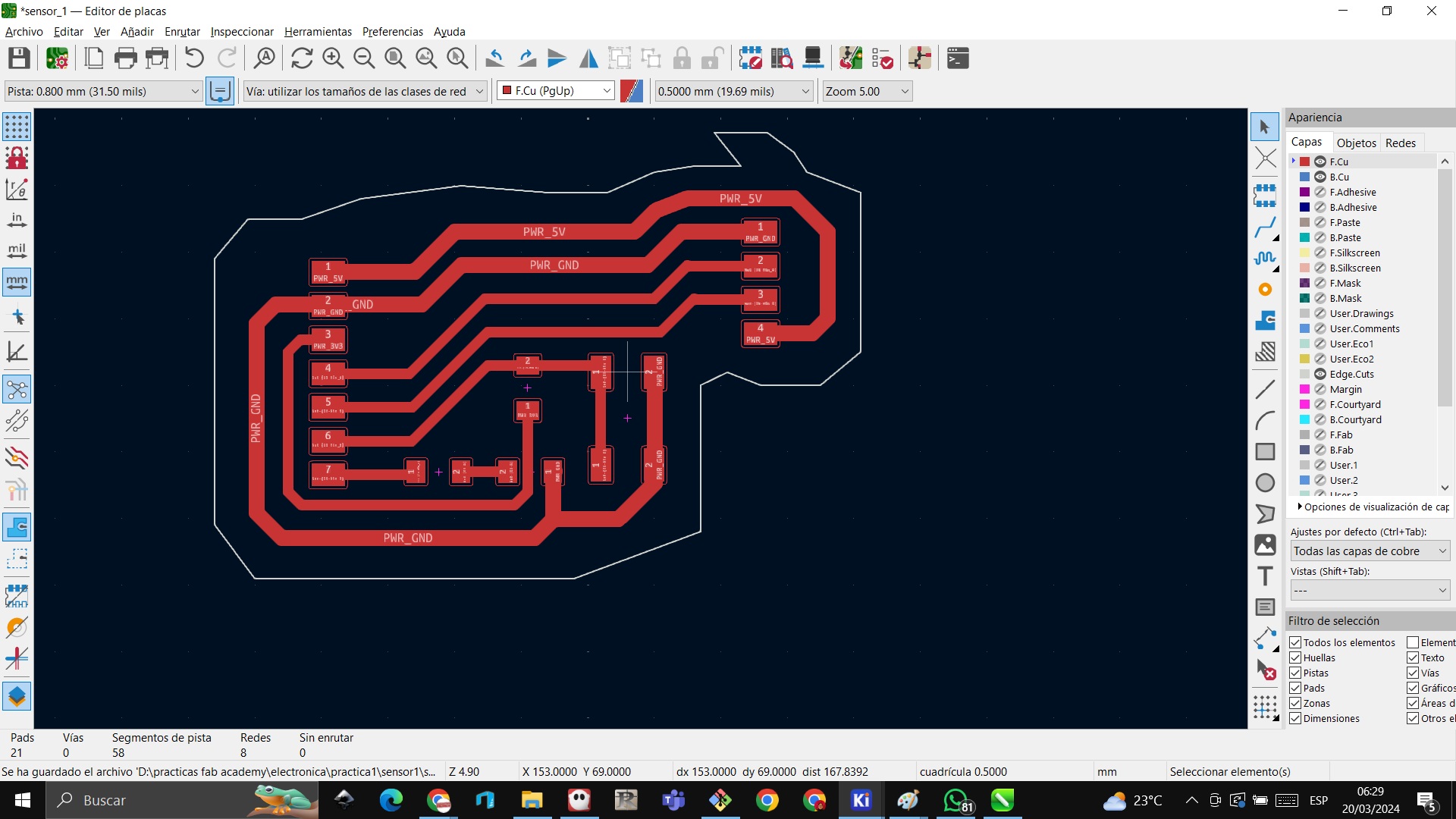
 STEP 38: We choose which track to work with in our case with the 1.2mm and then on the route tracks icon
 STEP 39: We click on a component and it automatically activates where to connect it
 STEP 40:They are left this way
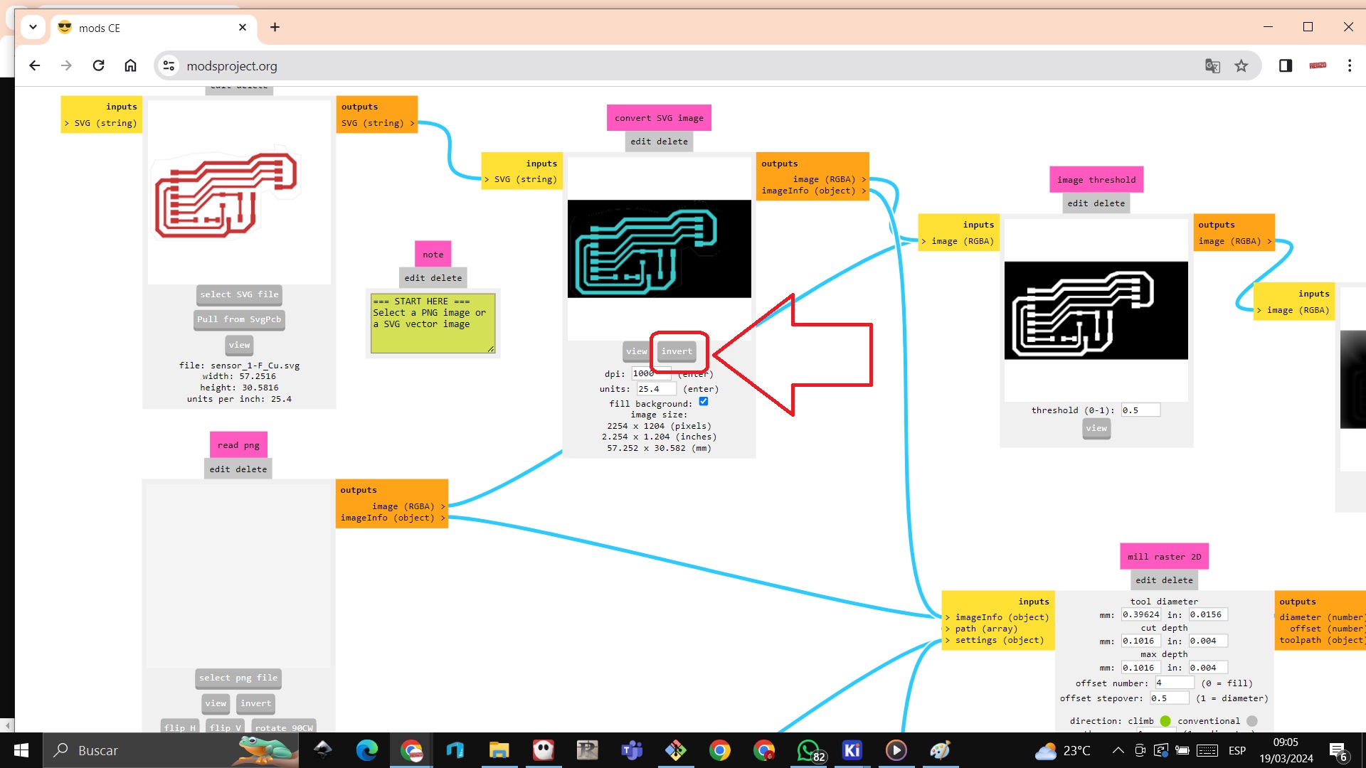
 STEP 41: Now we go to mill it, for that we have to go to appearance and we choose to show all the layers without copper
 STEP 42: We export in SVG
 STEP 43: We choose F.Cu and we already have the file
 STEP 44: We change the Switch from 2 pins to 4 pins and follow the same process
 STEP 45: Entering the updated switch
 STEP 46: Con el cambio del switch termino asi
 We now use mods project to be able to print the plate
STEP 1: We enter the url https://modsproject.org/ right click programs
 STEP 2: We choose WILL 2D PCB
 STEP 3: We enter the SVG file


 STEP 4: We open the SRM-20 milling machine software where we calibrate the X, Y, Z axes at their 0 point then click on CUT to load the gcode generated by the MODS

 STEP 5: We start the plate milling process
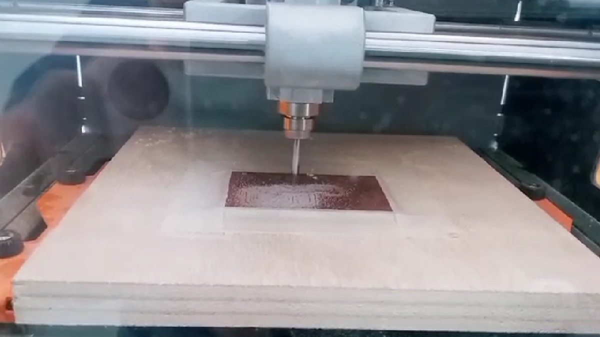

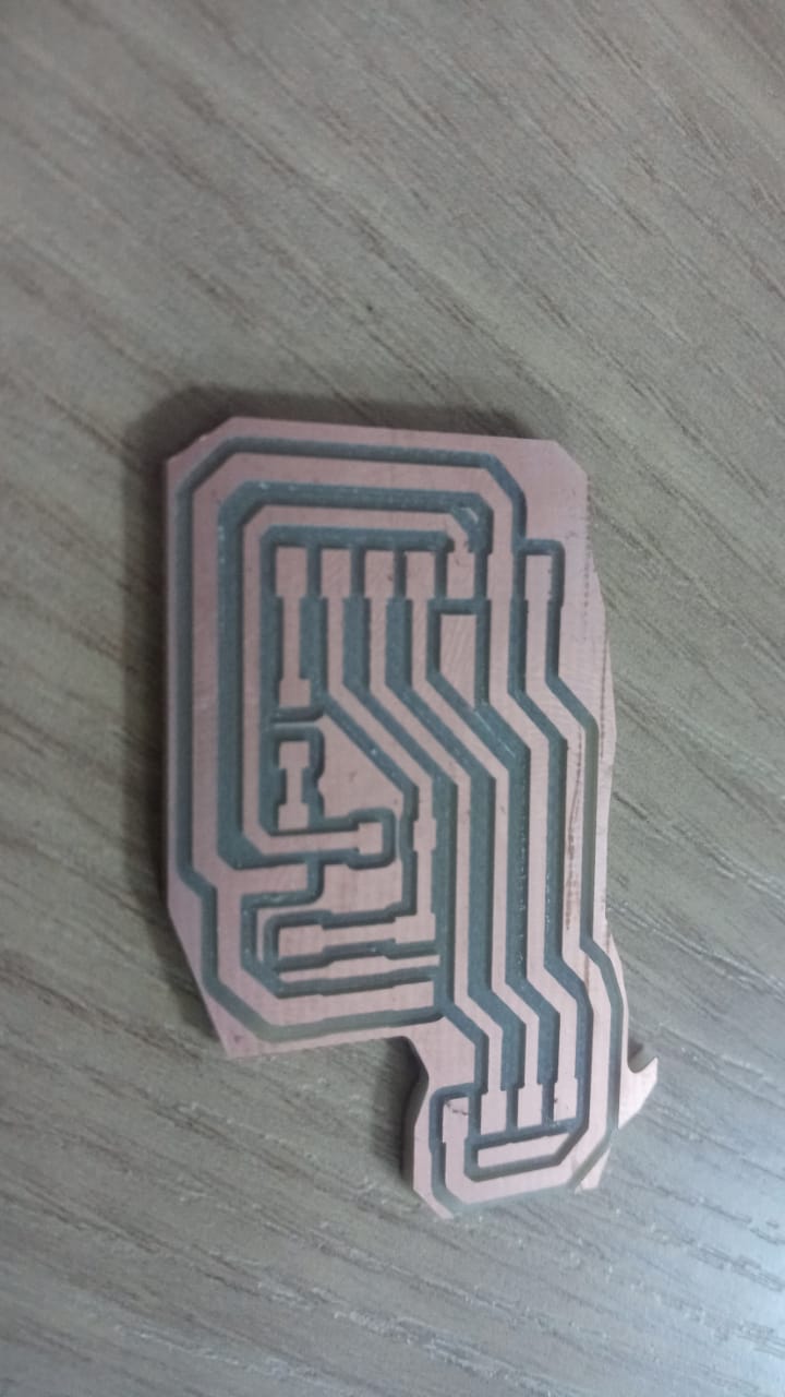
 After trying so much with strawberries and srm - 20

